5. Electronics production
This week I designed my own PCB, practiced surface mount soldering, and installed a simple blink code with Arduino. You can access all of my files here.
Lesson learned: multimeters are your best friend :)
Assignment
group assignment:
- Characterize the design rules for your in-house PCB production process: document feeds, speeds, plunge rate, depth of cut (traces and outline) and tooling.
- Document the workflow for sending a PCB to a board house
- Document your work to the group work page and reflect on your individual page what you learned
individual assignment:
- Make and test a microcontroller development board
Taking inspiration from Adrian Torres’ Fab Academy Planner, I made a spreadsheet with all of my tasks, deadlines, etc. This will allow me to stay on track for both my weekly assignments and my final project.
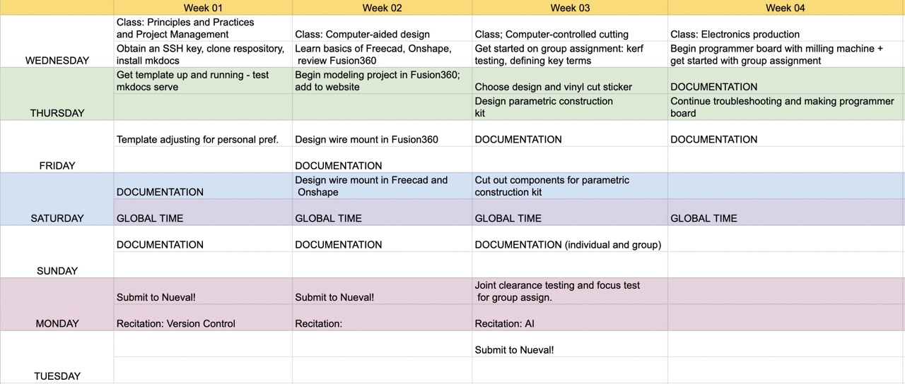
Here’s the schedule for this week. There isn’t much as of now because I’m not fully sure of the time frame for this week’s tasks.
Making the Programmer
Using Bantam Software and Milling the PCB
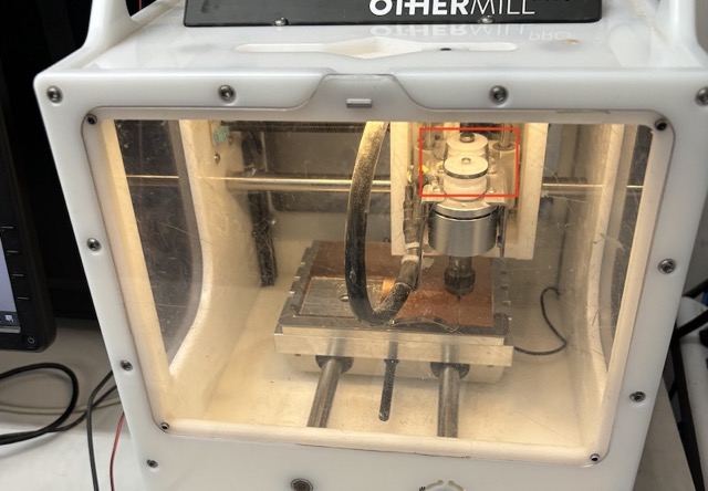
The first task of this week’s assignment was to use the Bantam desktop milling machine to mill a (pre-designed) PCB board. We planned to mill a FR-1 PCB that could work with a seeed xiao RP2040. This resource was really helpful in describing the settings/mill bits used.
Desktop Milling Workflow
I, alongside my peers, started by designing a workflow for the milling machine, under the instruction of Mr. Dubick. I have condensed it and rewritten it below:
Setting up the Bit and Fixturing
Before we set up the specifics in Bantam, we should first ensure that our bit is correct! We do this by using wrenches to loosen/tighten the collet that holds the bit in place.
-
Apply nitto tape or an alternative adhesive to the back of the material
-
Secure the material onto the bed of the milling machine
-
Remove current bit from the collet of the milling machine; use the 2 wrenches by the milling machine and align them respectively to the top of the spindle area and by the middle bit area where their imprints are. To loosen the bit, bring the top wrench clockwise and the bottom wrench counterclockwise Repeat this process until the bit is loose enough to take out.
-
Put the original bit back into its initial plastic container.
-
Insert and tighten your new milling end bit by bringing the top wrench counterclockwise and the bottom wrench clockwise. (similar to step 1). Repeat this process until the bit is secured.
-
Ensure that you select the correct bit in Bantam. Otherwise, your bit is liable to break.
-
When choosing which bit to use, start with the smallest bit (in this case, I used 1/64” first)
-
When inserting, leave around 1 inch of extra space between the bottom of the bit and the bottom of the spindle
-
Go to
Material setup > Install tool -
Set
z-offsetto 0.01 -
Configure the material size in x and y (measure your material with calipers)
Install Tool
Next, we have to communicate what tool we’re using (or at least what tool we’re using first!). To do this, we use the
install toolfeature in Bantam.
-
After clicking
Install tool, select the first bit thats going to be used- The spindle should move to the right of the bed; if it doesn’t manually jog it by changing the x-position
-
Once the spindle is hovering over the right of the bed (not the material), click
Startand wait for it to calibrate
Probing
Probing in the Bantam software is similar to focusing on a laser cutter; we do this to ensure that the z-axis settings are correct.
-
Move the side metal prong is on top of the plate
-
Select
material probeandZ-Stock only probe -
Jog the spindle to be on top of the material, specifically over the place you’re milling.
-
Click
Start; the bit will automatically go down to touch the material
File Setup
-
Open file; use the downloaded eagleboard/gerber files
-
For the
milling toolsportion, select all of the bits you’re using. For this assignment, I’m using:-
1/64” flat end mill for traces
-
1/32” flat end mill for second job
-
1/16” flat end mill for outline
-
-
Generate g-code by pressing
generate g-codeat the bottom of the screen; ensure no red marks, as red marks mean that bit is too big for the job -
Under toolpaths, ensure that
trace depth= 0.15 mm andtrace Clearance= 1.5 mm -
Additionally, under toolpaths, toggle/de-select the types of jobs you don’t need (i.e. holes, traces, outline)
-
Go to
Summary > Run Job, clickmill single fileandokto begin the job. -
Once it is done milling, move the bed to its
loadingposition, remove the window, and vacuum the excess material.
Now that we have this workflow, let’s begin milling!
Throughout this process, I worked with Alana Duffy, Ryan Zhou, and Landon Broadwell on the same document. We planned to mill four initial boards, followed by making additional backups.
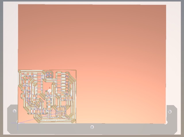
Here are the schematics provided by the QuenTorres guide and Dr. Taylor:
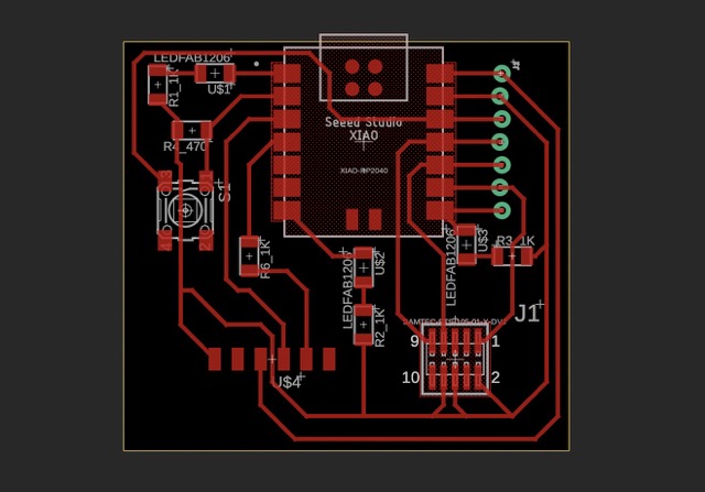
Here is the circuit schematic in Eagle, a workspace in Fusion360.
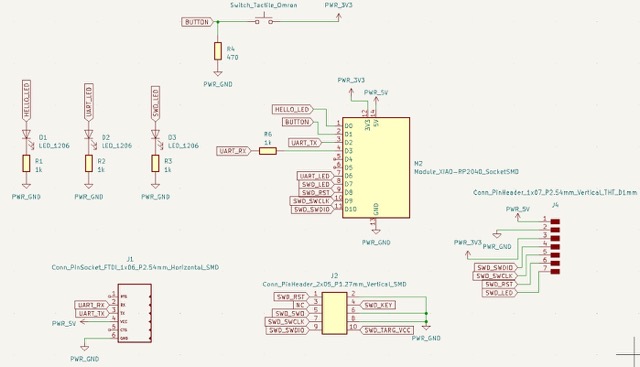
Here is the schematic provided in the QuenTorres documentation.
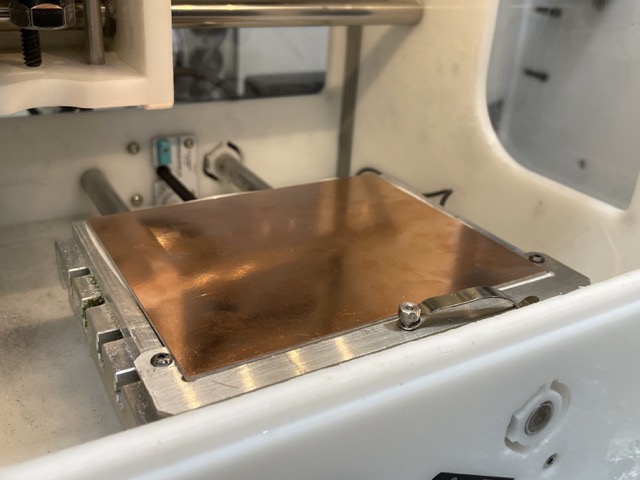
I first cut and applied nitto tape, a type of double sided adhesive, onto the back of the FR-1 PCB. I fastened it onto the bed of the milling machine.
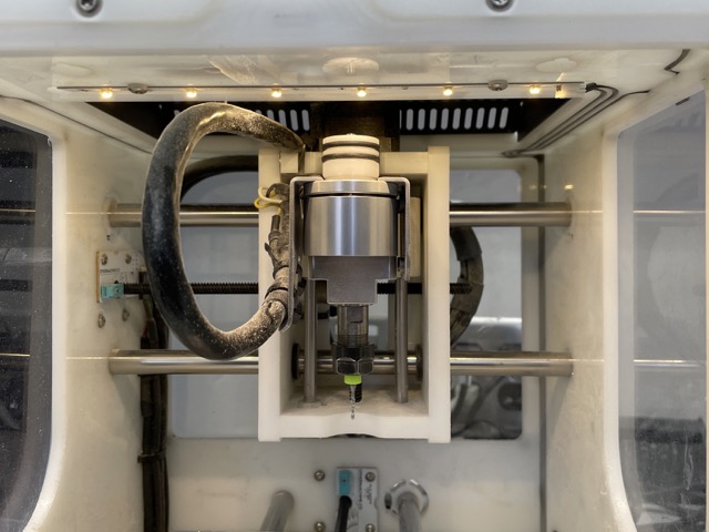
Next, I changed the bit to the 1/64”. I started by inserting the bit into the collet, leaving 1 inch underneath as advised by Mr. Dubick. I initially tightened the bit by twisting the collet to the right, before using the wrenches to ensure that it was fully secured.
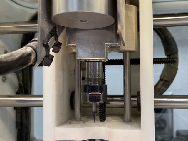
Here is the 1/64” bit installed.
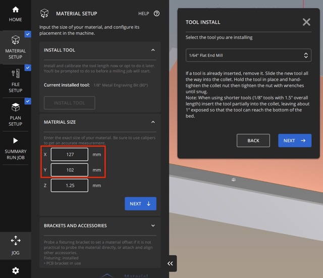
The next step was to configure the application’s settings. After opening up Bantam, I followed our workflow, importing the Eagle file and changing the file/material setup accordingly. The very first thing I did was install my tool. When I pressed the install tool button, followed by next, the spindle moved over the right side of the bed. I was initially confused as to why it wasn’t hovering over the material, but after consulting Mr. Dubick and Mr. Durrett, I realized that this process was taking the difference between the bit-to-bed distance and the bit-to-material distance to determine how deep the bit would go into the material.
Next, under file setup, I selected 1/64”, 1/32”, and 1/16” for my mill bits. This specific board did not require holes, so I untoggled it under toolpaths. Under material setup, the dimensions for the FR-1 were 127 mm x 102 mm (x, y).
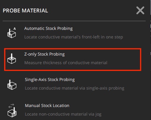
Now that my x-y dimensions were set up, I had to find the thickness in the z-axis. Previously, I had learned to do this with calipers, but today, we were taught a new method using the probe feature instead. Under the Material setup tab, I selected Material offset probing routines. This opened up a list of options, to which I selected z-only stock probing. I used the jog feature to move the spindle over an area I was about to mill and moved the bed’s side clip on top of the material. Pressing start, the spindle slowly lowered until the tip of the bit contacted the surface of the FR-1.
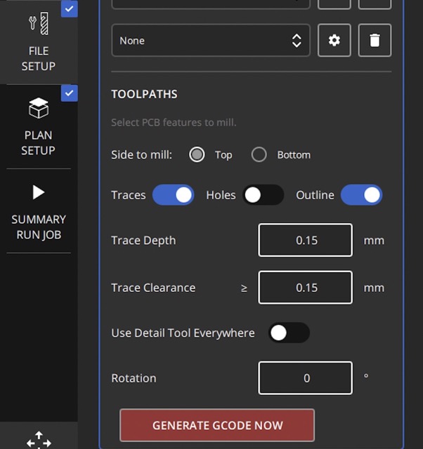
After configuring all of my settings, and inputting .15 mm for trace depth and 1.5 mm for trace clearance, I finally generated the g-code, which returned this model:
Generated g-code in the Bantam software
The final step was to move to the summary run job tab and to click mill single file. The software automatically manages when to switch the bit, so all I had to do was wait for the indicative message to pop up. Manually loosening the collet was a bit difficult, but I found that applying a short amount of force at the start and having a peer hold the bit underneath was helpful!
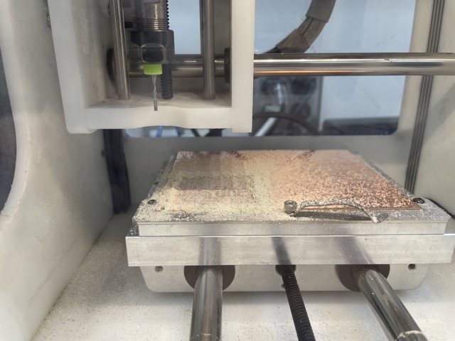
When the first job was complete, I vacuumed the surface off to remove the metal dust particles.
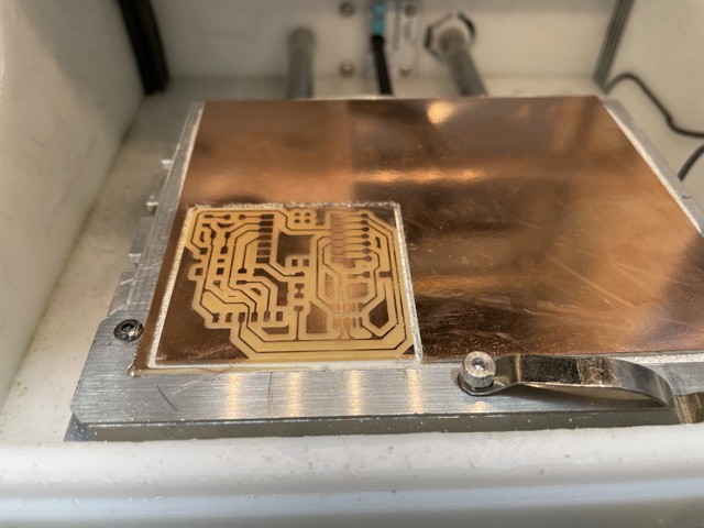
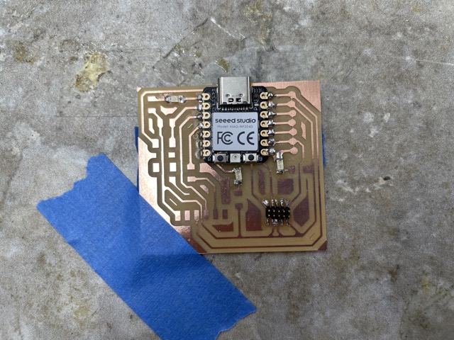
Phew! Here’s the first PCB! Time to do it 3 more times..
To adjust the position of the design, we changed the x and y coordinates under the manual placement category in the plan setup tab (z is kept constant). Here were the following dimensions for our four jobs:
- x = 4 mm , y = 3 mm
- x = 70 mm, y= 5 mm
- x = 70 mm, y = 54 mm
- x = 4 mm, y = 54 mm
Here is the milling machine tracing the fourth PCB as well as the software view.
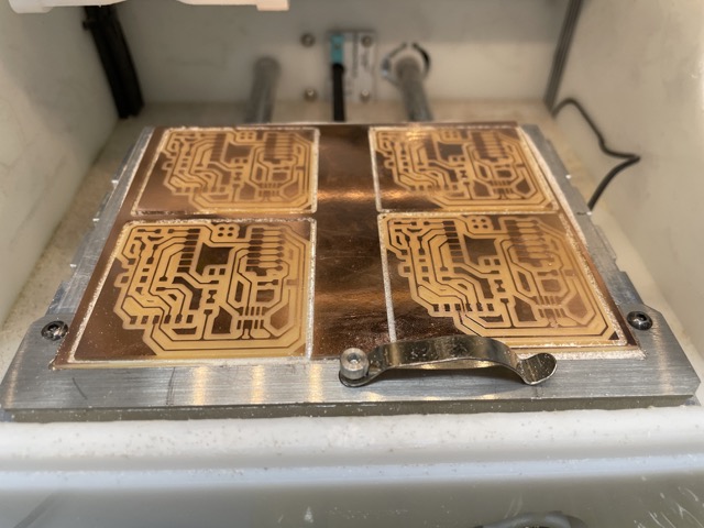
Here are the four PCB.
I cleaned the surface off with isopropyl alcohol and used a scraper to carefully remove it from the bed.
An issue that one of my peers encountered was the replacement of the rubber band around the milling machine’s motors. When these two bands (or just one), located above the spindle, snap, the job cannot proceed. When this happened on one of the milling machines, we immediately replaced the rubberband, wrapping it around the groove on the motors.
Typically, there are two rubber bands on the motor, in case one snaps. Here, there’s only one rubber band. Credits to Collin Kanofsky for the image.
Here is what the milling machine looks like with both bands in place.
Soldering Components to the PCB
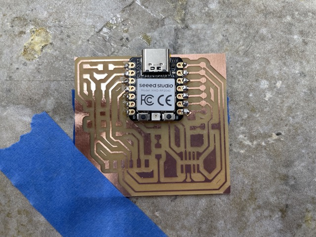
To insulate the back of the RP2040 (specifically the six exposed pads), I prepped it with a piece of kapton tape.
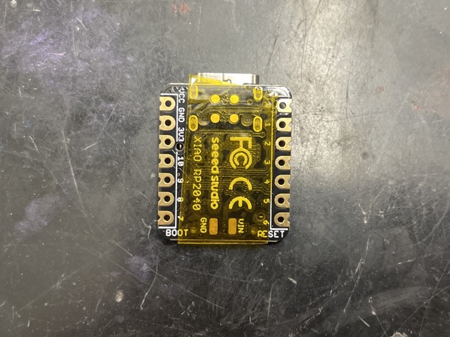
Here is the RP2040 with the kapton tape applied on the back.
Next, it was time to solder my components onto my PCB. I followed Adrian Torre’s QuenTorres board schematics as well as a provided file from my teacher and previous Fab Academy graduate, Dr. Taylor.
Components Used:
| Components | Quantity |
|---|---|
| Xiao RP2040 | 1 |
| Blue LEDs | 3 |
| Conn header SMD R/A 6 pos 2.54 mm | 1 |
| Conn header SMD 10 pos 1.27 mm | 1 |
| Tacile switch | 1 |
| 1kΩ 1206 resistor | 4 |
| 490Ω 1206 resistor | 1 |
| Milled PCB | 1 |
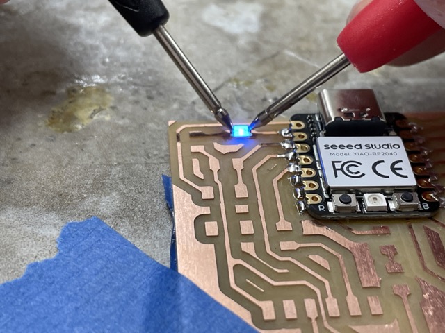
I set up my soldering iron and set the temperature to 650º. Usually, we would use 750º, but the traces cannot withstand such high heats.
I first soldered on the microcontroller. One of my personal goals this week, in addition to the weekly assignment, was to explore the different methods of soldering, so I used solder paste instead of the conventional solder wire. I applied a little bit of solder paste to the top left and bottom right corners to initially fasten the microcontroller in place, before going back in and soldering each pad. When heated, the gray solder paste turns into the silvery solder.
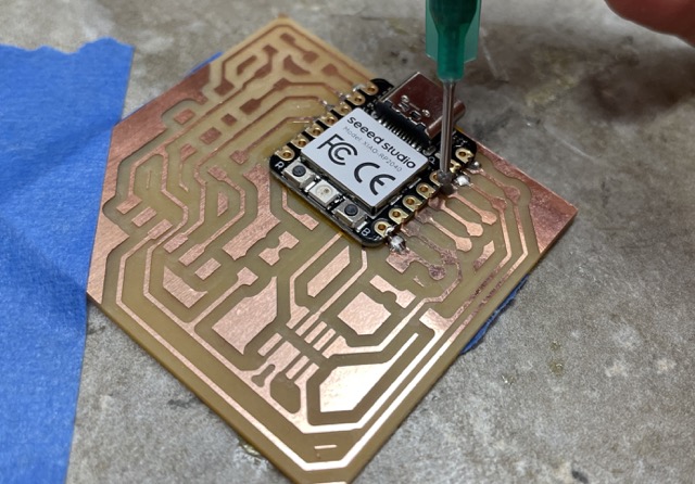
Applying the solder paste to the board
The next component I installed were the LEDs. Because LEDs have polarity, I had to ensure that the orientation was correct before soldering. With the help of fellow student Landon Broadwell, I examined the provided schematic in the Eagle workspace of Fusion360. Additionally, I used the multimeter with the diode setting (checks the power of the LED) and pressed the prongs to the ends of the LED.
Yay! The LED lights up!
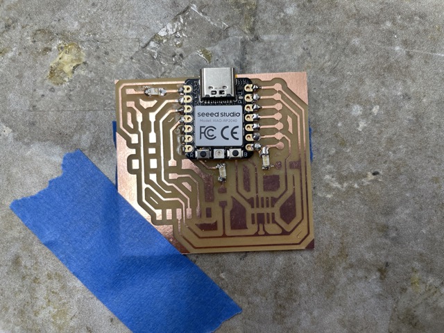
Generally, I had to be more careful with soldering these components on as to prevent a solder bridge.
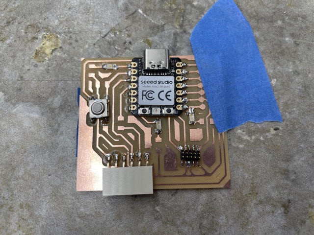
Conn headers and tactile switch installed
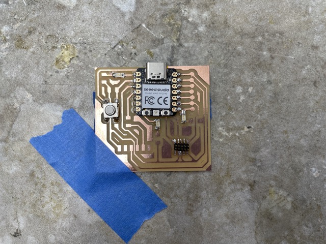
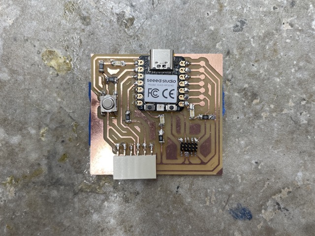
Finally, I added the two types of resistors onto my board (490Ω and 1kΩ). Unlike the LEDs, these did not have polarity.
The first issue I encountered was that the RP2040 wasn’t lighting up at all, indicating that power wasn’t delivered to the microcontroller. I checked the power supply by using the voltage setting on the the multimeter; when it returned 0 V, I knew that there was an issue with my soldering. To fix this, I observed my soldering under a microscope and fixed the areas that didn’t have a solid connection; this involved extending the solder along the trace as well. I did accidentally damage a trace during this process, to which I had to solder a stripped wire to supplement the connection.
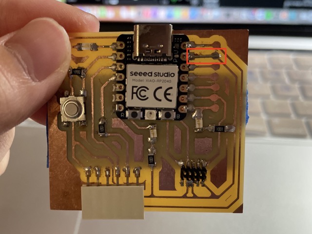
Here is board after fixing the damaged trace (with new and improved soldering too!)
Programming the Board
Simple Blink code and Troubleshooting
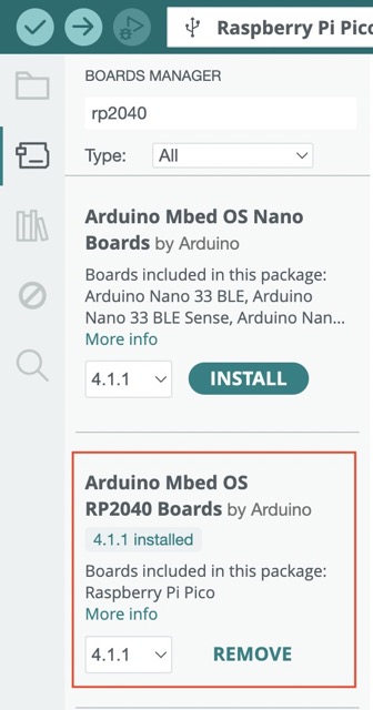
Upon downloading Arduino IDE, I first had to install the board I was going to use (RP2040). I opened up the boards manager, typed in “rp2040” and installed the Arduino Mbed OS RP2040 Boards.
Then, under the drop down menu at the top, I selected Raspberry Pi Pico as my board.
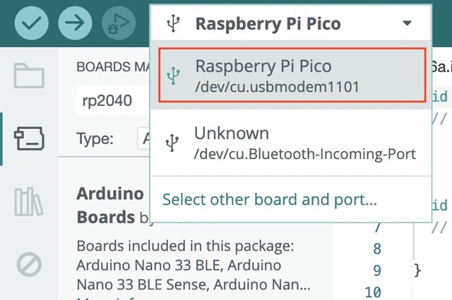
Note: I used a macbook to program my microcontroller, so the board installation process might be a little different.
Now, I could program my microcontroller! To start, I wrote a simple blink code with the three pins that the LEDs were connected to. Here’s what my code looked like:
void setup() {
  pinMode(26, OUTPUT); // initializing pin for LED
  pinMode(1, OUTPUT);
  pinMode(0, OUTPUT);

}

void loop() {
  digitalWrite(26, HIGH); // turn the LED on (HIGH is the voltage level)
  digitalWrite(1, HIGH);
  digitalWrite(0, HIGH);
  delay(1000); // 1 second wait
  digitalWrite(26, LOW); // turn the LED off
  digitalWrite(1, LOW);
  digitalWrite(0, LOW);
  delay(1000);

}
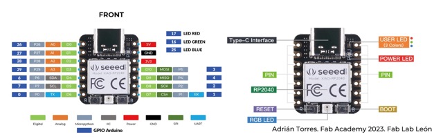
I referenced the RP2040 pinout, found from the QuenTorres page, to determine what these pins were.
Then, I selected Raspberry Pi Pico as the board to output the code to. Unfortunately, when I uploaded the code to the board (connected with a USB-C cord), only two out of the three LEDs were blinking, the third staying on the entire time. Confused, I used a multimeter to determine the amount of power coming from pins 3, 4, 2, and 1. Keeping my black probe on the GND, I noticed that all of these pins had a reading of 3.3 V (normally, the bottom pin that’s connected to the LED should be the only one, besides the 5 V pin, that has 3.3 V).
Because all of the pins had the same voltage reading, I originally assumed that the issue had to do with a solder bridge. Thus, I tried applying flux to the soldered areas to reposition the RP2040; when this failed, I similarly tried to use the heat gun at 239ºC. To my dismay, I was still unable to move the RP2040 around, so I decided to start again with a new board.
Thankfully, my peers and I milled extra boards in case of an emergency. Taking one of these boards, I followed the same process of taping the RP2040 and soldering it to its respective copper pads on the PCB. This time, Mr. Dubick advised us to test the voltage coming from the different pins first, before soldering any more components on. Again, the same readings of 3.3 V came from every pin. Now, I was frustrated and confused, but I knew that my issue wasn’t necessarily a solder bridge.
After 2 more hours of troubleshooting (pure struggle), Mr. Dubick discovered that there was an accidental trace connect between the different pins on the FR-1 board itself. I promptly removed this connection by running a thin razor along the copper.
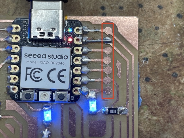
Board with trace issue (left) and fixed board (right)
I uploaded the code again, and it finally worked!
Now the LEDs are synchronized!
Here’s a general procedure I created afterwards for installing components and troubleshooting:
-
Solder the microcontroller onto the board
-
Run a simple code that supplies power to the active pins (i.e. a blinking code will work)
-
Placing one probe of a multimeter on the GND and the other on a pin, determine if power is supplied correctly. If it is, then proceed with soldering; if it isn’t, check for solder bridges and arbitrary traces on the PCB.
Programming the Buttons
The next task was to make the LEDs manually blink when the button is pressed. I made three main adjustments to the blink code: 1) initializing the pin connected to the tactile switch, 2) using the digitalRead() function to determine whether the button was on or off (HIGH or LOW), and 3) writing an if-then statement for when the button is pressed. This resource was super helpful in learning basic syntax for C++.
Here’s my updated code:
int buttonstate = 0;

void setup() {
  pinMode(26, OUTPUT); // initializing the LEDs
  pinMode(1, OUTPUT);
  pinMode(0, OUTPUT);

  pinMode(27, INPUT); // initializing the tactile switch

}

void loop() {
  buttonstate = digitalRead(27); // returns whether button is on or off
  if (buttonstate == HIGH) {
    // turn LED on:
    digitalWrite(26, HIGH);
    digitalWrite(1, HIGH);
    digitalWrite(0, HIGH);
  }
  else {
    // turn LED off:
    digitalWrite(26, LOW);
    digitalWrite(1, LOW);
    digitalWrite(0, LOW);
    }

}
Here are the LEDs blinking when the button is pressed.
Group Assignment
The group assignment this week was to characterize the design rules for the PCB production process on our Bantam PCB Milling Machine, encompassing document feeds, speeds, plunge rate, depth of cut (traces and outline) and tooling. You can find our full documentation here
Individual Contribution
I revised the group PCB CNC workflow so it was more streamlined, and I created the chart of terms/definitions. Regarding the line test, I also ran the second iteration and documented that portion of the site.
Reflection and References
Thank you to Adrian Torres and his QuenTorres documentation, Teddy Warner, Mr. Dubick, Mr. Durrett, and Dr. Taylor’s additional resources for help this week. This was one of the most challenging weeks so far, but their guidance made the process a whole lot easier.
This was the first time I produced a PCB, so I was a bit nervous to get started. However, I ended up learning a ton about the milling machine’s features, and I’ve explored new methods for surface mount soldering. During the process of milling 4-5 identical copper boards, I became a lot more comfortable with the milling machine prep process, alongside switching out the different bits. In terms of soldering, I really liked the efficiency of solder paste, especially for smaller components!
The most challenging part of this week was definitely the troubleshooting aspect: at times, I felt like there was no other way to solve an issue other than restarting the process over and over again. However, with patience and guidance (and a multimeter), I was able to figure out why one of the LEDs remained on constantly.
Overall, most tasks this week were tedious, but it proved to be just as rewarding when I finished.