
Electronics Design
Individual assignment
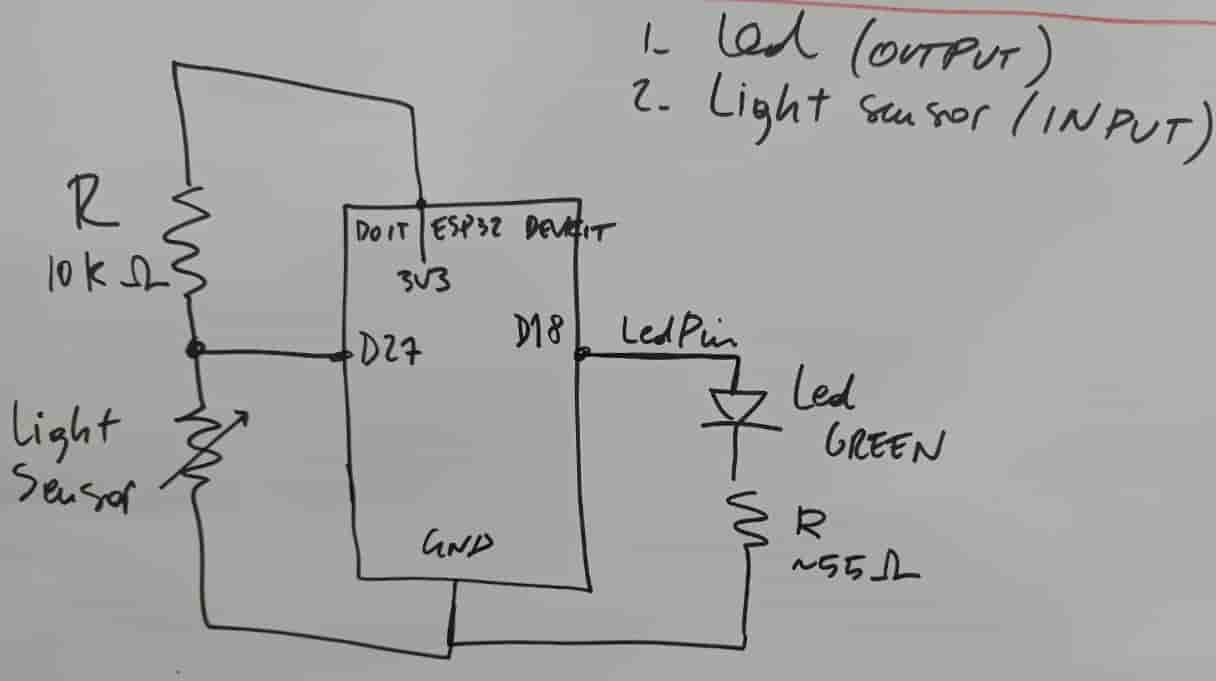
For this week, I learned how to make a schematic drawing for some circuits, and to do this, First, we should define the purpose of the circuit and what is the main component needed to make such a circuit, like what MCU needs to work with or other components, the ESP-WROOM-32 had to sketch the circuit with pen paper as shown below:
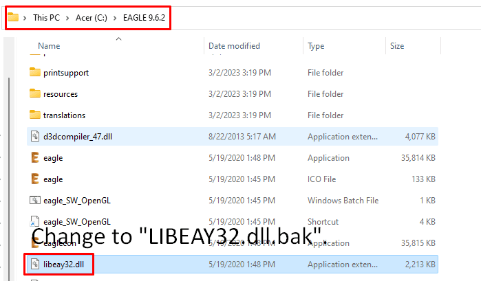
I have decided to work with Eagle Software, which is a software program used for designing printed circuit boards (PCBs). It allows users to create schematics and layouts for electronic circuits, which can then be manufactured into physical PCBs. So I have downloaded it, but unfortunately, when I run the software it crashed and it did not opened so I searched on the Autodesk support page, and I followed one of the steps and thanks god it worked:
I opened the program file in my computer, then I searched on the "LIBEAY32.dll" and changed it into "LIBEAY32.dll.bak" then I have restarted the computer and opened the software again.
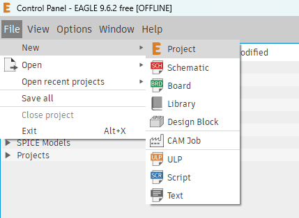
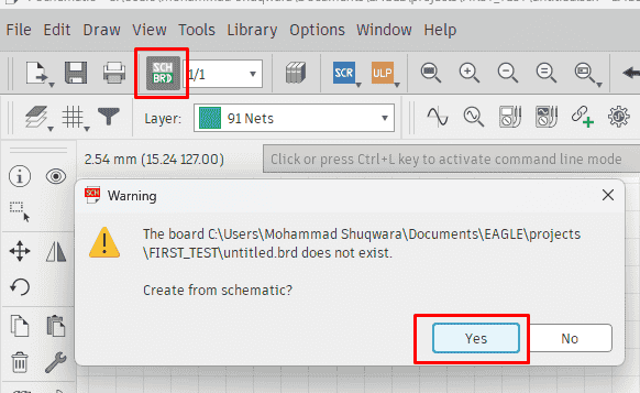
To start a new project I have navigated to File > New > New project and I named it as First test:
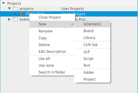
Then to start drawing I navigated to project > First test > New schematic:
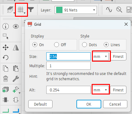
First thing I had to do when I made a new schematic is to enable grid, to help while drawing, and I had to make sure the dimension if the grid is in mm so I had to stich with this size, so I navigated to grid shape on the tools menu > change the grid size to 2.56 mm where the "Alt" value allows me to set a second, alternate grid size that can be used alongside the default grid because sometimes a different grid size is needed for more precise or complex work, and I can switch between the default and alternate grids by pressing the "G" key on your keyboard:
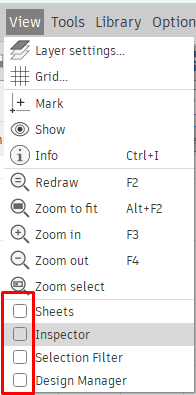
To make the schematic looks more comfortable I had to turn off the non needed tabs, from view > uncheck the selected ones:
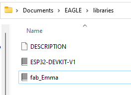
After I prepared the canvas of the schematic, now it is the time to start drawing, but still before I had to install the FAB components, and the ESP-WROOM-32 library. After I downloaded them I copied them and navigated to Documents > Eagle > Libraries and pasted them:
unfortunately the fab library did not show the schematic of the component, and thanks to our instructor Emma, she edited the files but she was not able to modify the main library but it could be downloaded from here.
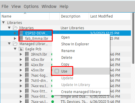
Now to activate the libraries, from control panel of eagle, I navigated to Libraries > user libraries > Right-Clicked > Check on Use.
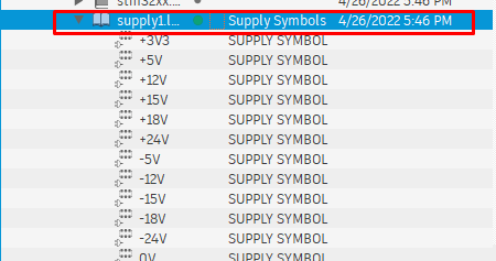
Sense till now I only need supply1 library from eagle library, and to not get confused with all libraries I navigated to Managed Library and uncheck all then search on > Supply1 > check on.
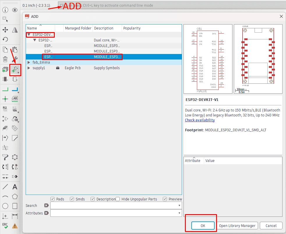
To start adding components, I could write "add" on the command bar or from tools bar, navigate to add part > choose the library > choose module > ok.
it is important to make sure that I am using the correct foot print as shown on the right below:
After adding all components, I could rotate any part by right-click on the component or from the tool menu or just type rotate on the command bar, also it could be to change the name of the parts, add value or even move or delete all of those command could be written on the command bar:
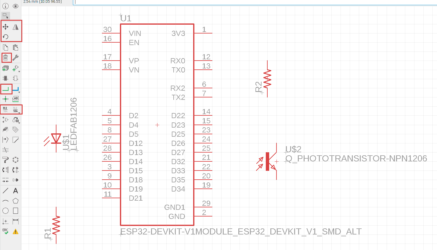
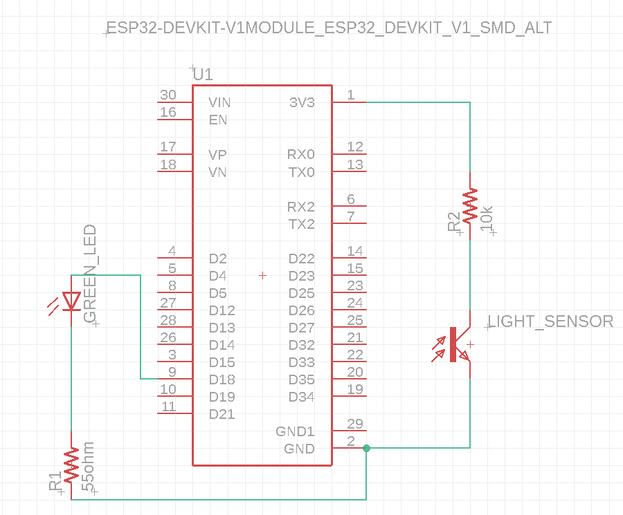
To connect the parts with each other, just typed net on the command bar then I connected between components:
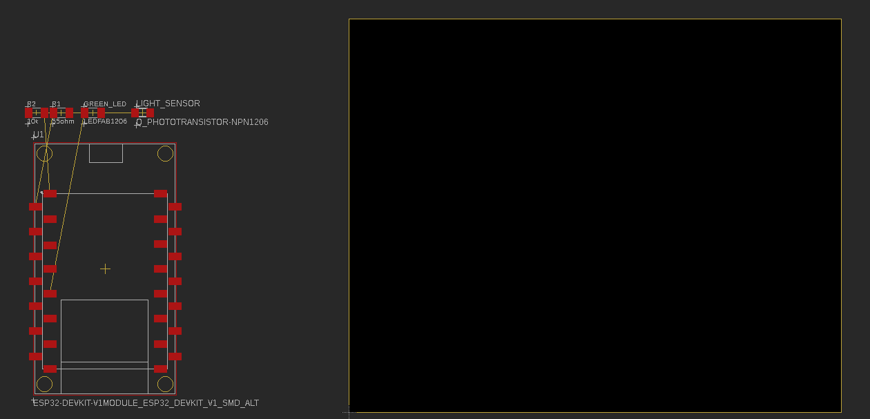
To prepare the board for milling, I had to switch to the board by clicking on the icon shown below then click ok:
When the board opens it looks like as shown below, the yellow border means it is the PCB board size, and it could be edited from the moving tool on the tool bar
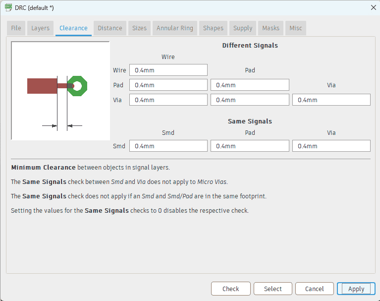
The yellow wires called airwire and in order to arrange the components and make the traces, there is a useful tool called autoroute, which automatically rout the airwires, but before I should define the minimum thickness of the trace, and to do this from view > DRC(design rules) > Clearance and I changed the values to 0.4 then apply:
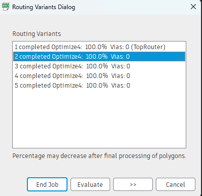
To autoroute the wire from the tool bar > autorouter then continue :
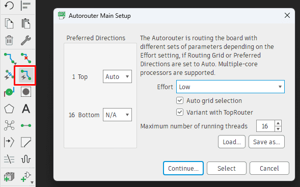
The autorouter gives multiple routes possibilities I chose the second one then I clicked on end job:
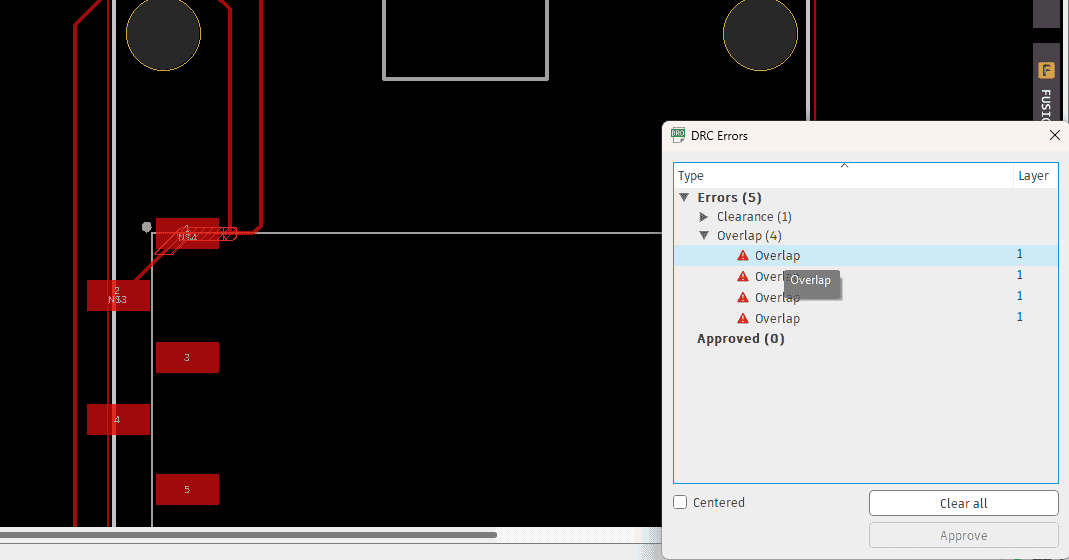
In order to make sure that there are no errors in the routes, from tools > Error > and it showed some overlaps and I moved them by the move tool from the tool bar:
The First design trial was looks like:
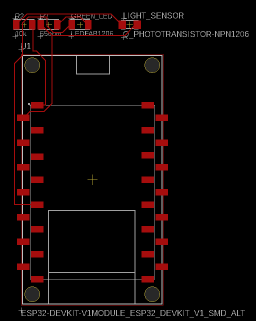
After I discussed the first trial with our instructor, Emma, she told me that the lines was thin to be milled and try to avoid locating some components under the type c port, so I added a switch to control the led then rearranged the components as shown below:
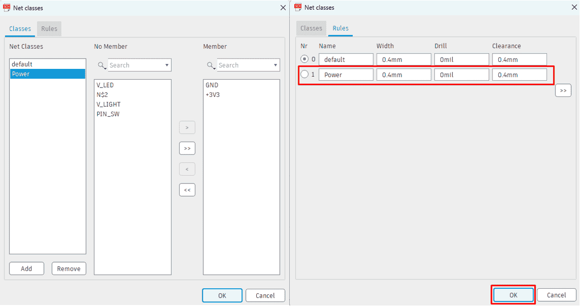
To set the thickness of the traces I navigated to Edit > Net classes > and added the names of the nets then navigated to Rules and set the value 0.4mm:
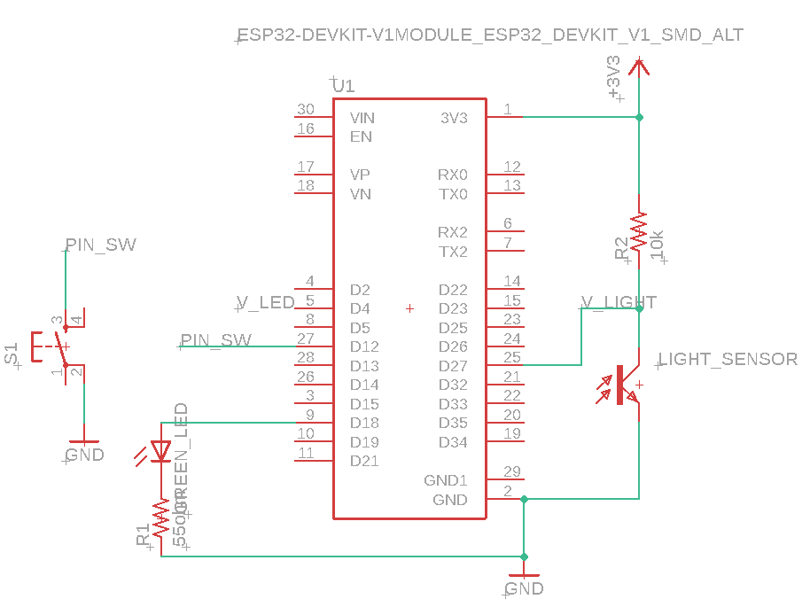
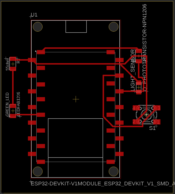
The final design looks like:
Group assignment
- Use the test equipment in your lab to observe the operation of a microcontroller circuit board (as a minimum, you should demonstrate the use of a multimeter and oscilloscope).
-
Document your work on the group work page and reflect what you learned on your individual page.
For the group assignment we had to use different equipments in our lab, which was the multimeter,power supply and, oscilloscope.
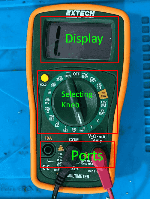
The multimeter is an electronic measuring tool that is capable of measuring various electrical properties of a circuit, including voltage, current, resistance, capacitance, and continuity. It is typically composed of a dial or digital display, test leads, and a selection switch to choose the mode of measurement. Multimeters are widely used in electrical and electronic engineering, as well as household electrical applications, for the purpose of troubleshooting, repair, and maintenance of different electrical devices and systems.
Every multimeter have 3 main components which are:
- Display: This is the part of the multimeter that shows the measurement readings.
- Selection Knob: This component allows us to select the type of measurement to be taken, such as voltage, current, resistance, capacitance, or continuity. and it have additional settings for different ranges of measurement.
-
Ports: These are the sockets on the multimeter where the test leads are plugged in. There are usually two input jacks, one for the positive (red) test lead and the other for the negative (black) test lead. The input jacks may also have different settings for different types of measurements.
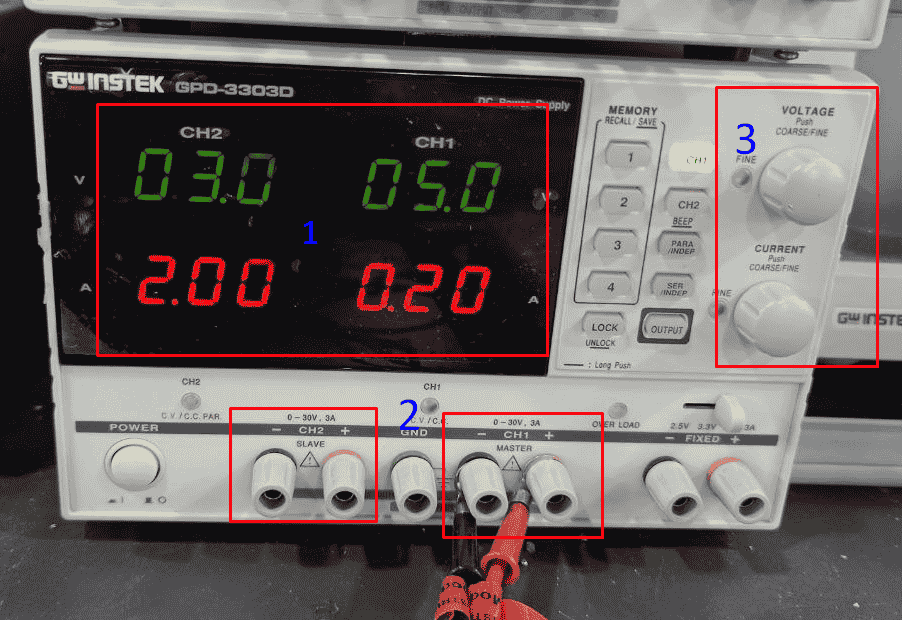
The second tool is the regulated power supply which is an electronic circuit or device that provides a stable output voltage or current, regardless of any fluctuations or changes in the input voltage or load conditions. It is typically used to power electronic devices or circuits that require a stable and precise power supply, such as microcontrollers, amplifiers, and digital circuits.
It consists mainly of 3 components:
1- The display which shows the voltage and current values.
2- The output ports, each channel have 2 ports, GND and VCC.
3- The controlling knobs, which controlling the output values of the current and the voltage.
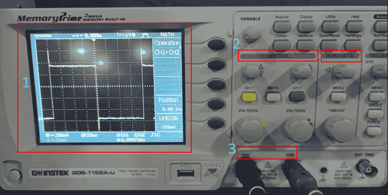
Third tool is the oscilloscope which is an electronic test instrument used to graphically display and analyze various electrical signals. It is a device that allows us to see the waveform of an electrical signal, such as voltage or current, over time.
It consists mainly of 3 components:
1- The display which visualize the wave form.
2- The vertical and horizontal section. The vertical which used to control the amplitude, or height, of the waveform. while the horizontal controlling the time base, or width, of the waveform.
3- The probes, which are used to sense the voltage or current of the signal.
After we learned how to use the instruments, We initially used an Oscilloscope in order to observe the operation of the MCU process, so we created the circuit containing a Potentiometer and a LED, then writing a sketch using Arduino programming, and saving it onto the development kit. After connecting the circuit to the Oscilloscope, we discovered that the initial reading was incorrect. Upon further investigation, we realized that the sketch required a "map" value to enable the Potentiometer to provide an accurate reading.
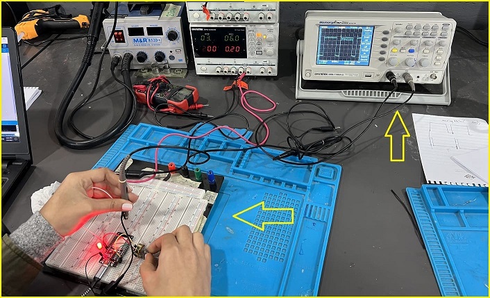
The video below how the circuit works, note that when we lower the Potentiometer value, the led brightness increases and the current would increase and that is why we see the signal arise, while when we increase the Potentiometer value the curren drops down and that is because no current flows to the led.