8. Electronics production
This week I manufactured a circuit board with CNC milling and soldering the components by hand.
I did test the board for short circuits with a multimeter. I programmed and did further testing for the board in the output week.
Group work
For this weeks group work we milled testing boards using the mods and the Roland SRM-20 in our Fab Lab.
While I like the idea of using one software to make the toolpaths for all the machines the idea of using png files instead of grbl just seems weird.
We managed to make the boards with the Roland but that just made me appreciate the fact that we can use the LPKF machine for the boards for our individual assignments. The process for that seems just so much more "professional".
Even though the Roland is a very accurate small CNC machine The height adjustment is just too delicate with the V-bits. Of course there are those nice things like the automatic tool change in the LPKF.
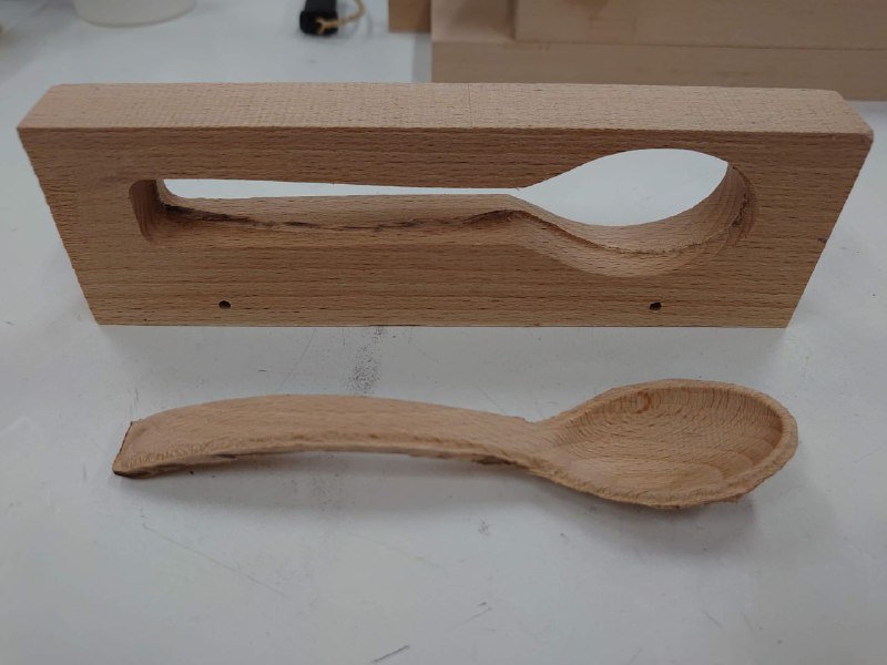
I prefer to use the Rolands for machining small pieces from wood like spoons. For that the precision is a little overkill but helps to create a good surface finish.
Exporting GRBL from KiCad
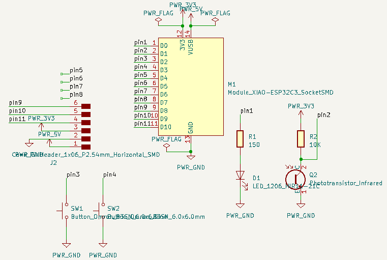
I made some changes the board which I designed in week 6 before milling it.
Here is the updated schematic
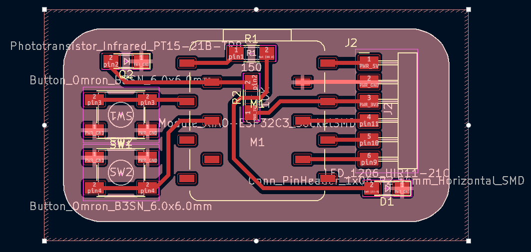
And the PCB layout.
Here are the KiCad source files.
To export the necessary files from KiCad:
- File > plot
- Select F.Cu and Edge.Cuts
Milling
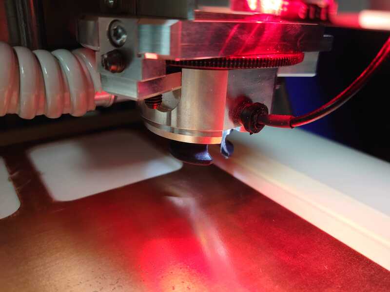
For milling the board I used the LPKF machine in our Fab Lab. It's a commercial machine but really powerful once you get the hang of it.
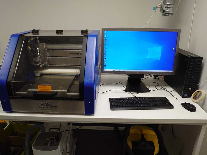
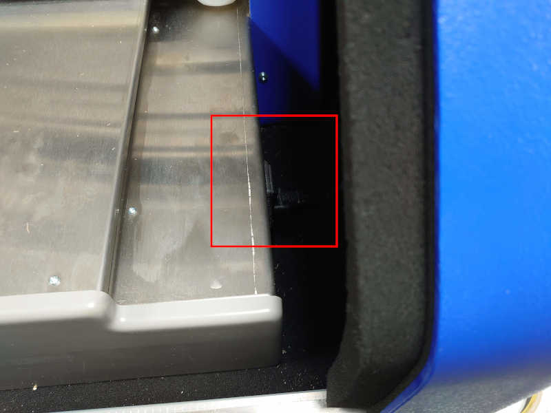
The power button is hidden away inside the machine enclosure.
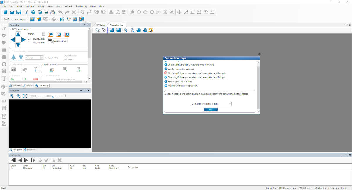
After turning the machine on I would start the CircuitPro program for the LPKF.
Here it is just asking which tool it's currently holding, check and confirm.
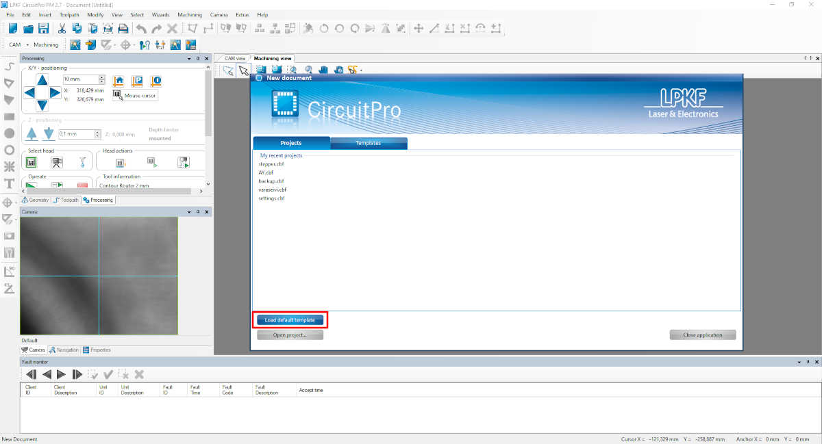
Click on Load default template.
On the top there is this tool bar. To mill a circuit board you need use these tools in order from left to right.
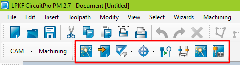
However, some of those are skipped as they are not always needed.
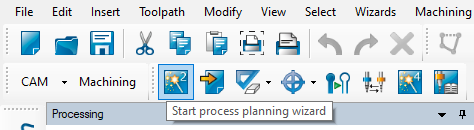
Process planning wizard
Starting with the first one.
Click next.

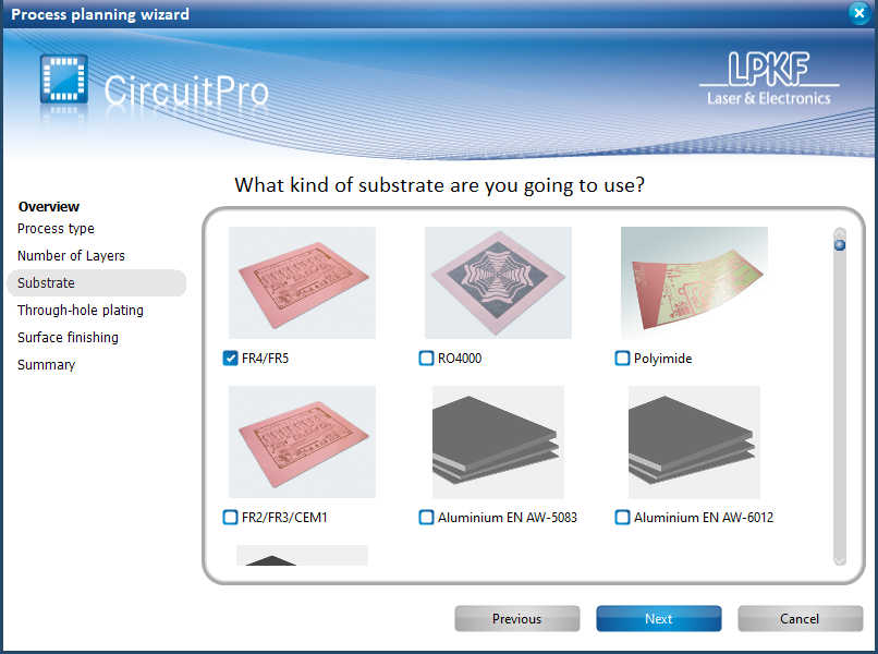
Select Single-sided top.

I was instructed to just go ahead with the FR4/FR5 option even though I think the material usually used is FR1 or FR2.
Import files
Next step is to import the files that were exported from KiCad previously.
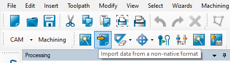
Select the "Edge cuts" and "Front copper" .grbl files.

And make sure the program understands them correctly.

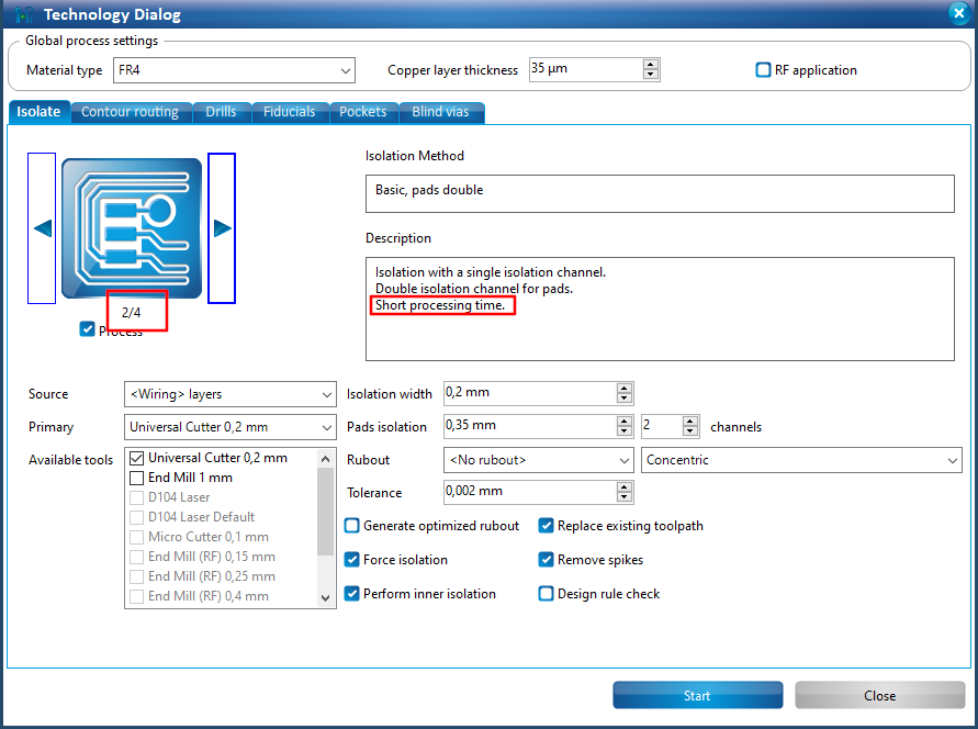
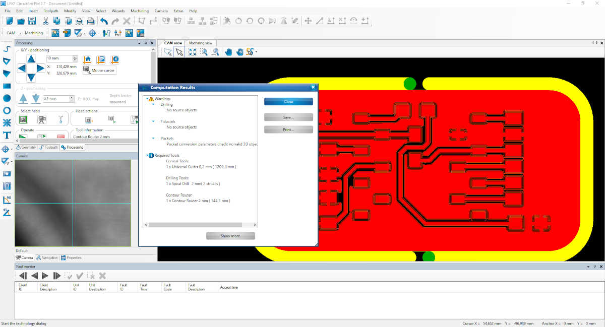
Generate toolpaths
Then the actual toolpaths can be generated.

I changed the highlighted settings.
The position of the tabs.

And here is the result.
Board production wizard
Now the actual production starts.

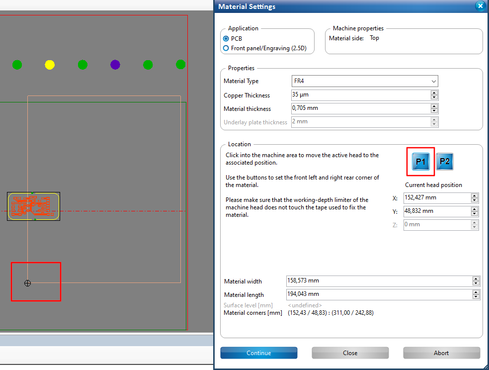
Time to mount the material.

Here is the machine table.

I selected this piece which has some bad cuts on the middle but I am positive that my board would fit in the corner.
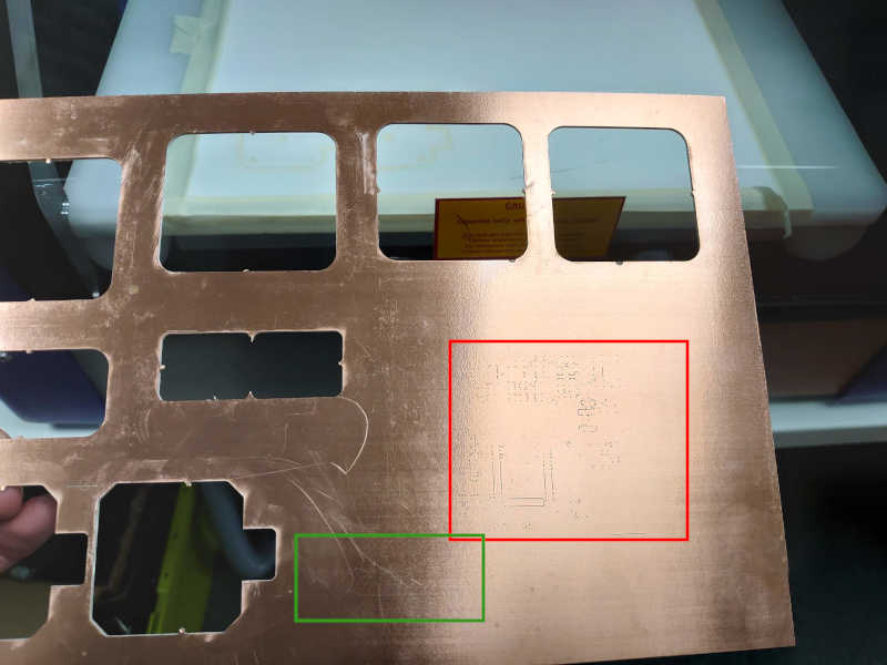
We will later see that it just barely fit.
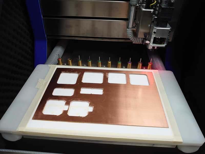
The board is place on the table.
And taped from the edges with masking tape as is instructed in the software. This helps to secure the workpiece in case the vacuum doesn't work or something.

Next I set the area in which I could machine the board. For this I ignored the previous shallow cuts on the board.
Here is the first corner in the software.
And in the machine itself.

Note: the black "foot" of the machine must not overlap with the edges or any tape!
The second corner.
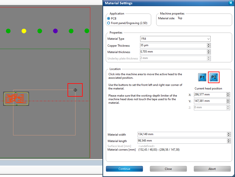
Top right.
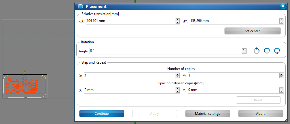
After that is done the board can be placed inside the rectangular perimeter that was just defined. It can be dragged with the mouse and rotated from the menu if needed.
In the next step the machine will Mill a Line to calibrate the width of the cut. This needs to be adjusted as the tool wears down.
Before clickin on the button drag the line somewhere where it doesn't consume the board more than cutting the current board would. So best place is usually on the board you are cutting. This time I did it on top of the previous markings/shallow cuts on the board.
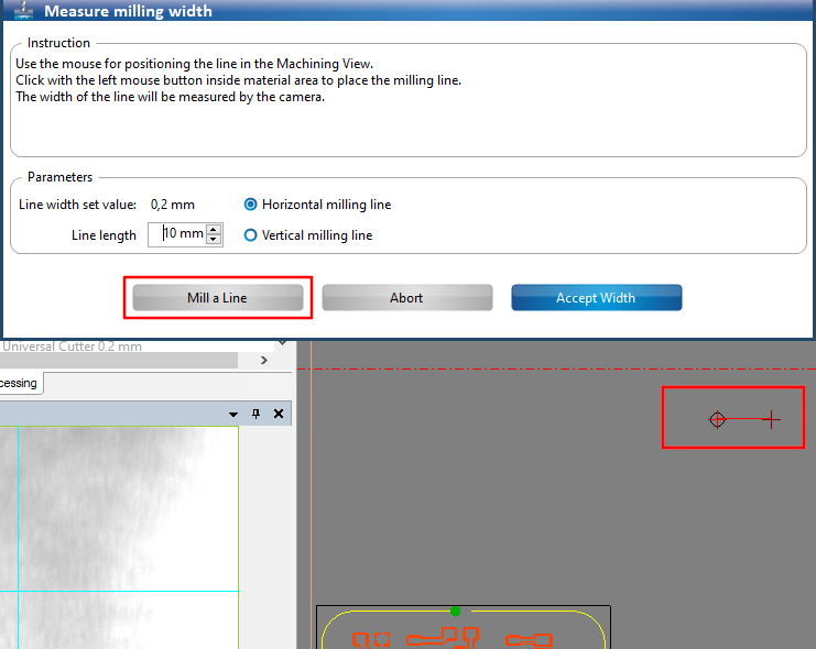
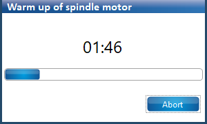
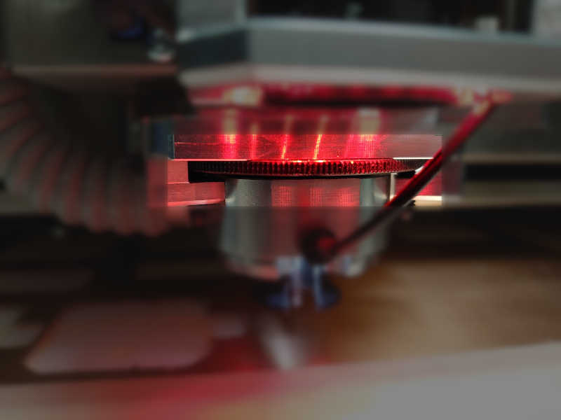
After clicking Mill a Line the machine will cut it after warming up.
Here you can see the line that was cut. The other markings do not matter for the measurement.

The machine will autofocus after cutting the line.

You can see highlighted the camera view on the bottom left is now in focus.

The software will try to automatically measure the line but it's often inaccurate. Instead use the Point to Point measure mode.
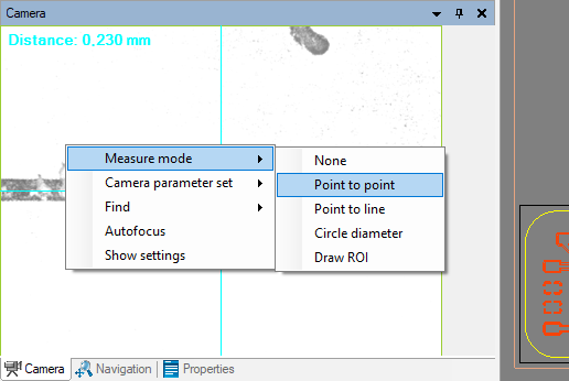
Drag the line from the edge of the cut to the other edge perpendicular to the cut. Do it in a spot you can clearly see the edge of the cut.

The result here is 0.230 mm which is exactly what we want.
If the line is not acceptable width spin this wheel to adjust the height and mill a new line to measure.
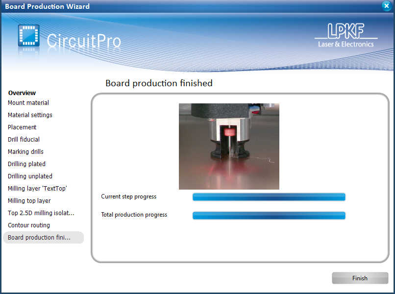
After the width is correct click Accept Width and the machine will start the operation.
Milling in progress
The software will show the progress.
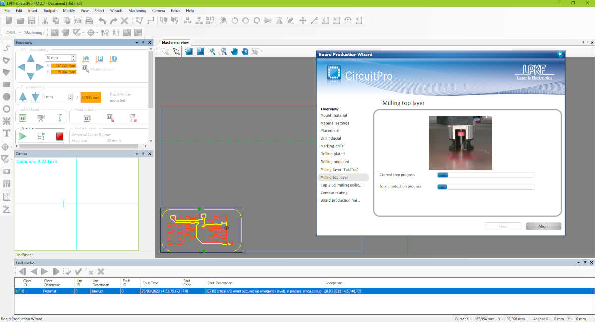
Here it's already cutting the contour of the board which is the last operation here.

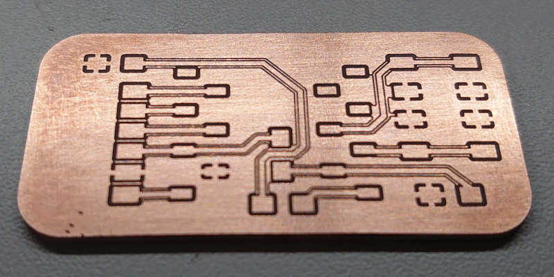
And the board is milled!
However, ther is some post processing we want to do before that.
Milled circuit board
Here you can see how close the markings were to my board. Luckily I didn't have any important or small traces on that part of the board. And even if there were, those small dots would be unlikely to cause an issue.

Then I snapped the board off, filed the tabs and rubbed it with steel wool to remove the oxidated copper. Then I just vacuumed it and washed with water to clean any fine dust off.

Inspecting the board with a microscope reveals no obvious shortcircuits or other faults. However, there are these double lines due to the option I used at this section. While that shouldn't cause an issue it still looks weird and is unnecessary. A better option would have been to use another option which removes all of the unused copper. For that the machine usually uses 1 mm endmill in addition to the V-bit and that could actually be much faster than this "Douple pads". I just chose the double option as it said "short processing time" and the first option (single pass) didn't look suitable.
Soldering
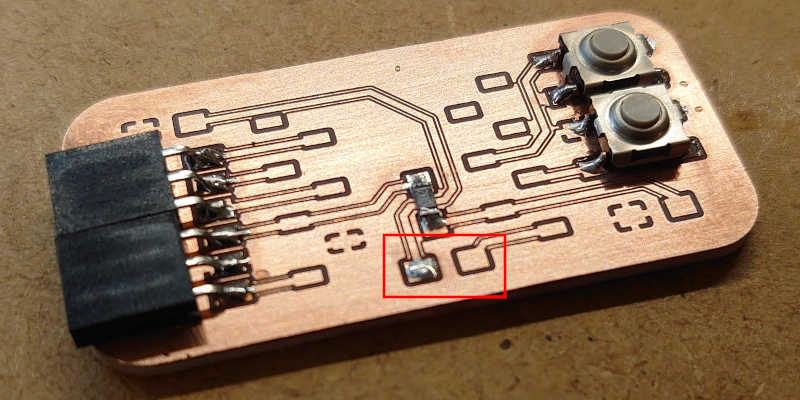
Now the board is ready for soldering.
I did all my soldering manually with the soldering iron as my board has only a few small components.
Soldering small components
This is a trick I learned from the staff to solder small components.
- Melt a small dot of solder on the contact.
- Place the component (here a resistor) with tweezers on top
- Melt the solder with the iron while holding the resistor in place.
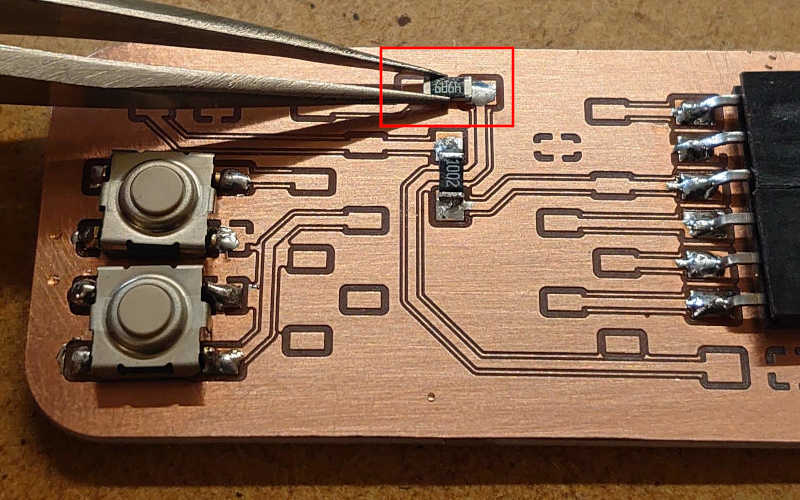
- Finally solder the other contact of the component.
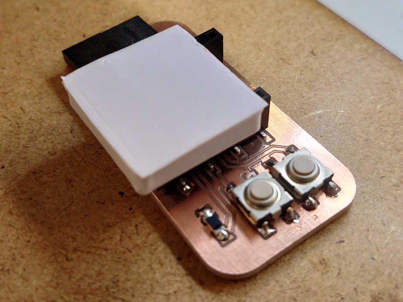
3D printed jig
As we use the vertical pinheaders to connect the microcontroller those need to be placed accurately paraller.
You could just use the microcontroller board itself but then you need to be sure that those pins are soldered straight in case you want to change the microcontroller board.
For that I quickly designed and 3D printed a bunch of these simple "jigs".
Here I have only soldered one of the pin headers.
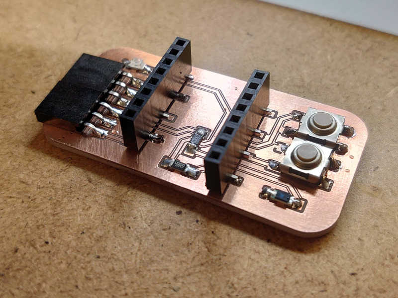
And then placing the jig over helps to align the pin headers while soldering.
The good
Most of the solderings were good (enough)

But that wasn't always the case..
The bad
This one joint would have been a short circuit.
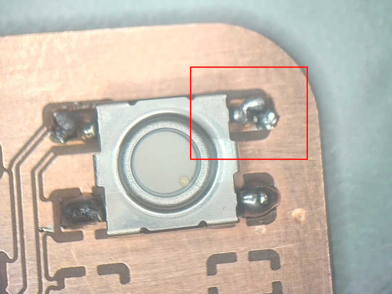
But I was able to fix it just by poking with the iron.
The ugly
But it wasn't pretty. I think the solder was heated too much too often. It's not shiny at all.
Also you an see the other joint below formed a kind of a ball on top more than melting in the surface. I was told this was likely because the copper wasn't heated enough.
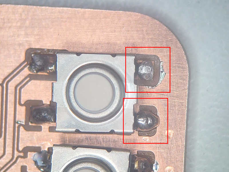
I wouldn't trust those joints to hold that well but both of them are redundant so it shouldn't matter after I fixed the short circuit.
Result
And here is the result. Overall I think the board turned out nice.

You can compared it to this PCB layout presented also earlier.
Here also again the KiCad source files.
I did test the board for short circuits with a multimeter. I programmed and did further testing for the board in the output week.
End of week 8.