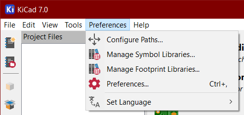
6. Electronics design
This week I designed the first prototype of the PCB I could use in my final project.
The three Seeed Xiao boards presented in week 4 do have the same physical footprint and atleast the power and ground pins are the same. Therefore It should be possible to use any of the boards with the development board. For now I expect to be using the ESP32C3.
Group work
From this week's group work I learned the general level of power usage for the microcontrollers we are dealing with and how the peripherals can affect it. It was surprising to see that even the very small built in led draws a measurable current (~0.3 mA). In contrast, the NeoPixel at full white draws about 11.7 mA.
Not much more to add as the measurements were quite simple.
Designing a board with Kicad
Kicad is an open-source PCB design software.
The plan is to design an initial prototype PCB that could be used in the final project. The PCB will have pin connectors so the separate microcontroller can be pulled off and changed if needed. Kind of like a "shield".
I have used Kicad once before and then I got great help from this tutorial video. Just note that the video is made with an older version. Our local lecture mostly covered all the same things with the newest version.
To my understanding the workflow goes roughly like this:
- Design schematic
- Assign footprints
- Arrange footprints
- Route traces
Setting up
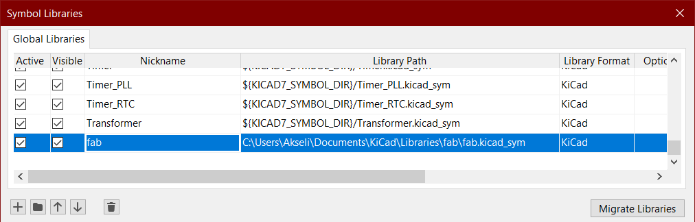
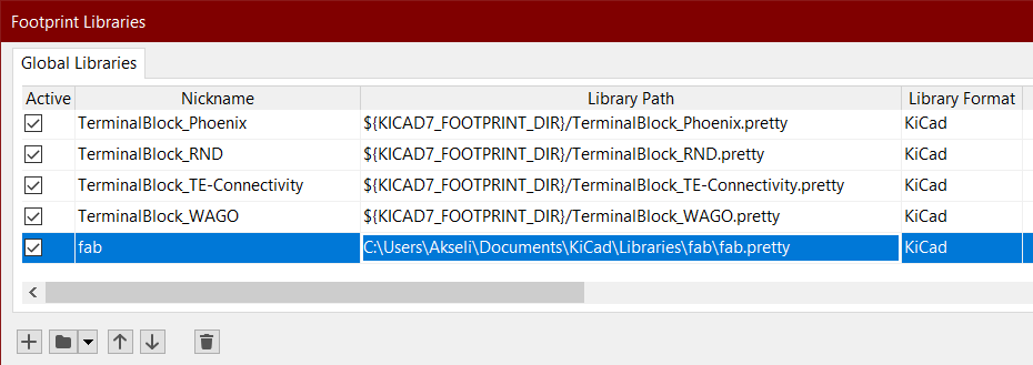
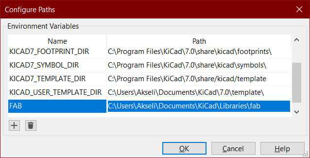
After installing Kicad I downloaded the Fab electronics library and did the steps in the repos readme:
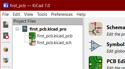
After that I created a new project and it looks like this:
Designing the schematic
So the first step is to open the Schematic editor.
Adding components
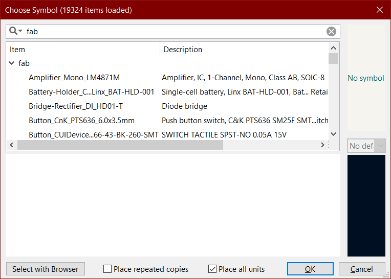
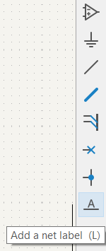
Adding component symbols is done by pressing the shortcut A or by the tool on the right panel.
With the tool active clicking on the page opens the symbol selection.
Searching "fab" and expanding the correspondent dropdown reveals the components in the fab electronics library:
First I want to add the ESP32C3:
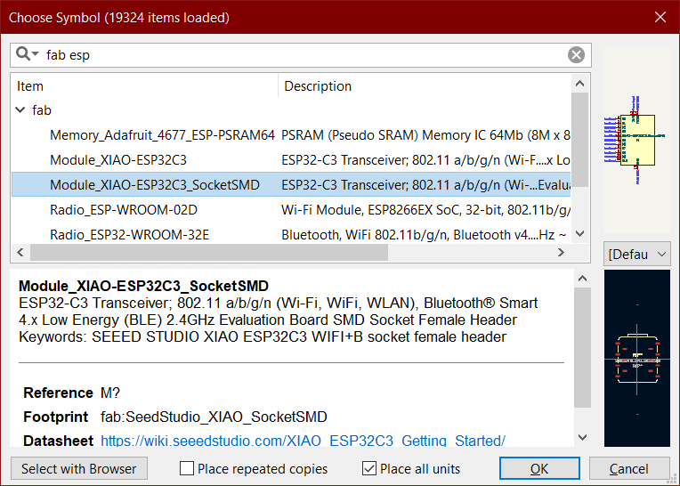
It also shows the preview of the footprint there. I want to select SMD one because the boards for surface mount components are faster to manufacture.
Clicking Ok allows placing the component symbol with mouse.
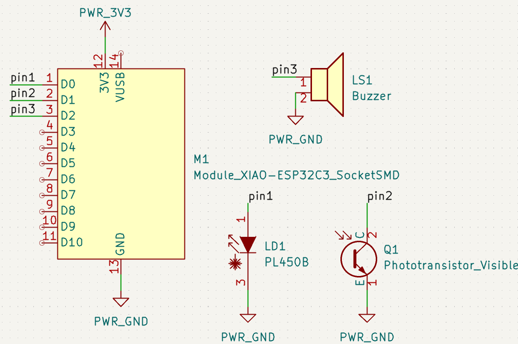
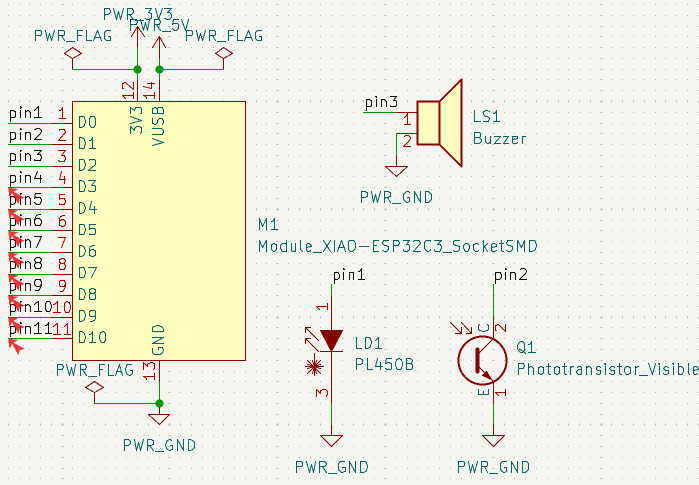
After that I placed also the other symbols which I think my final project would need. These are not yet the exact parts I will use as that will be specified later.
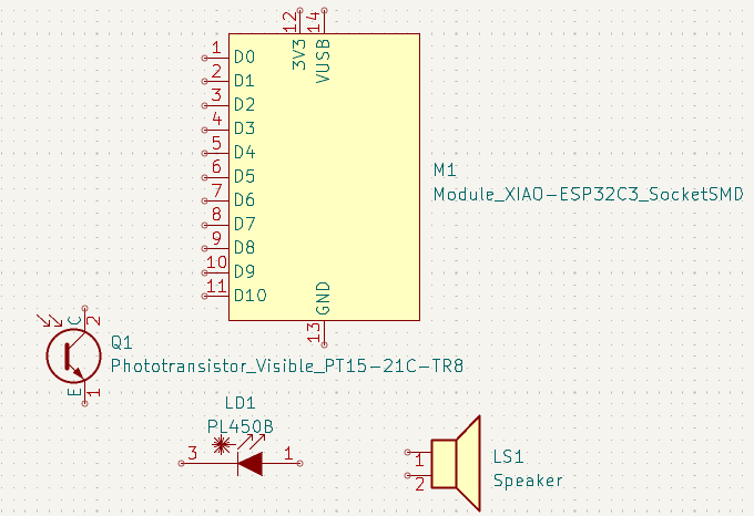
The components are:
- Microcontroller
- Laser (not from the fab library)
- Phototransistor
- Generic speaker
The component symbol can be rotated with R and flipped with X when it's selected.
Connecting the pins
After adding the components I of course needed to add the ground GND and power 3V3 symbols too.
The pins can be connected directly with the wiring tool W
but using "labels" the schematic will stay much cleaner.
This keeps especially the more complex schematics readable.
And here are the connections:
When we think it's ready we want to focus on the top bar.
symbols
Starting with this tool:
But apparently Kicad 7.0 does this automatically or something as it just completes instantly:
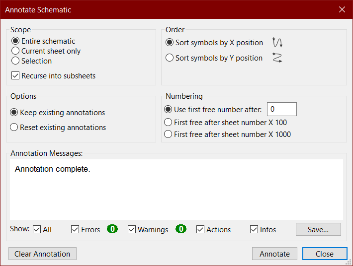
Maybe if something was wrong then this would still be needed.
electrical rules check
Next is this one:
It seems that something needs to be fixed. First is this error:
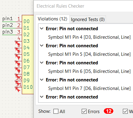
So every pin should be connected to something. I could add an extra pin header to connect these pins to. Even though that could be useful if I later come up with something else i need I can make a new board then. So I will ignore this problem but I added labels to the pins anyways.
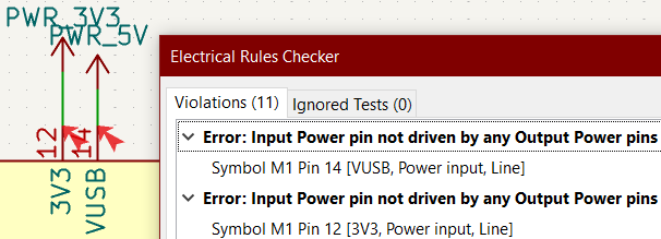
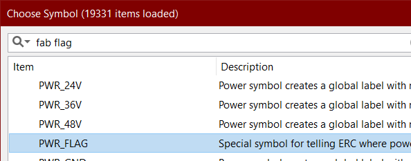
This is solved by connecting this PWR_FLAG to each of the power symbol,
including ground.
And here is the finished schematic:
Assigning the footprints
Still not finished with the schematic editor.
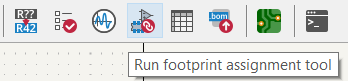
This does what it says. It seems that Kicad 7.0 has done this also automatically. However we might need to change the footprints for certain components. Here is the menu for that tool:
On the middle you can see the components and on the right the valid footprints for that. You can also filter those footprints as is highlighted. Double clicking applies the footprint to the component.
When ready click Apply and Ok.
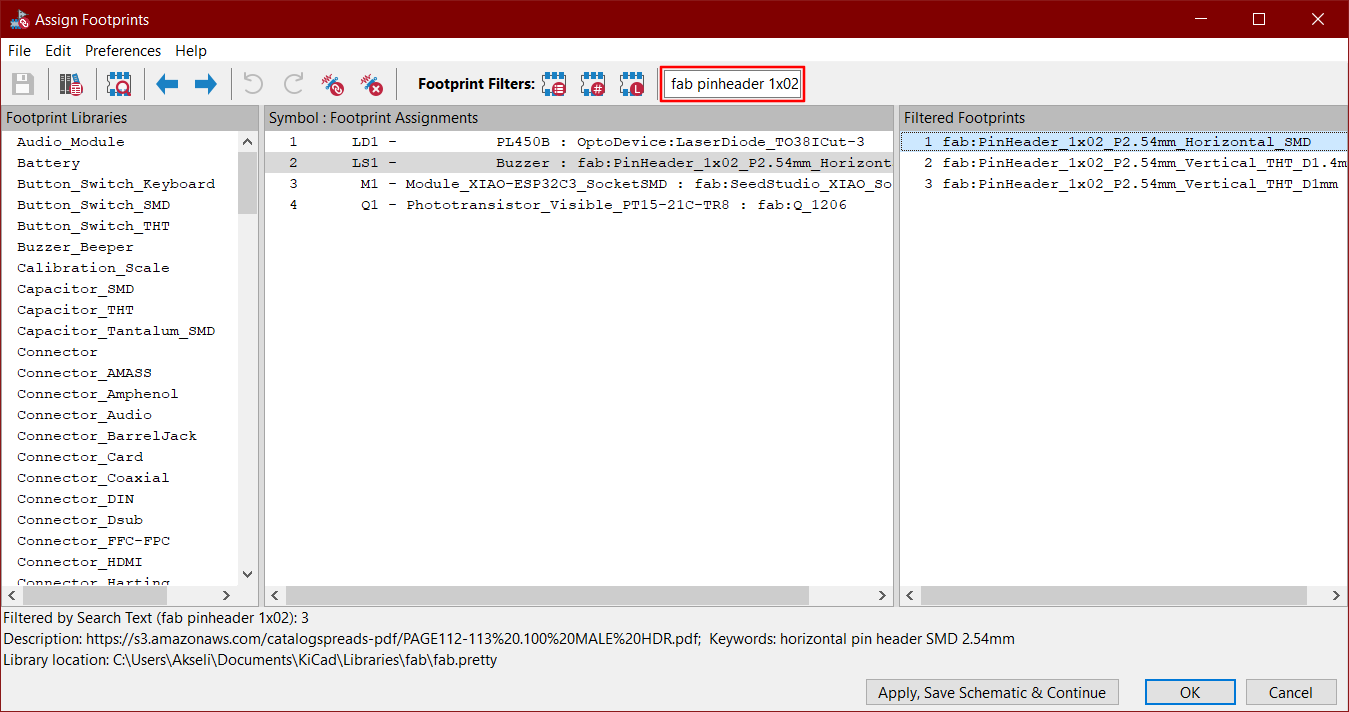
Then open the PCB editor:
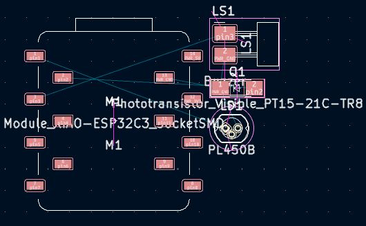
Designing the PCB
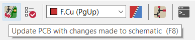
This is where the physical layout of the board is designed. First step is to update the PCB:
This just puts all of the components in one clump:
Before doing anything else I will define the borders of the board.
Defining the board perimeter
First select the layer Edge.Cuts:
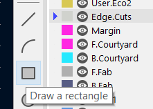
And draw a rectangle
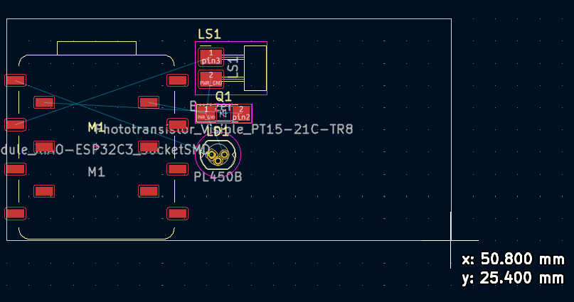
Optionally the board can be also more complex. To get rounded corners draw the edges with lines leaving space for arcs.
Placing the components
The lines that connect the pins are called the ratsnest. It provides guidance when positioning the components.
Now the goal is to place the components so that the pins can be connected. The same controls apply as in the schematic editor.
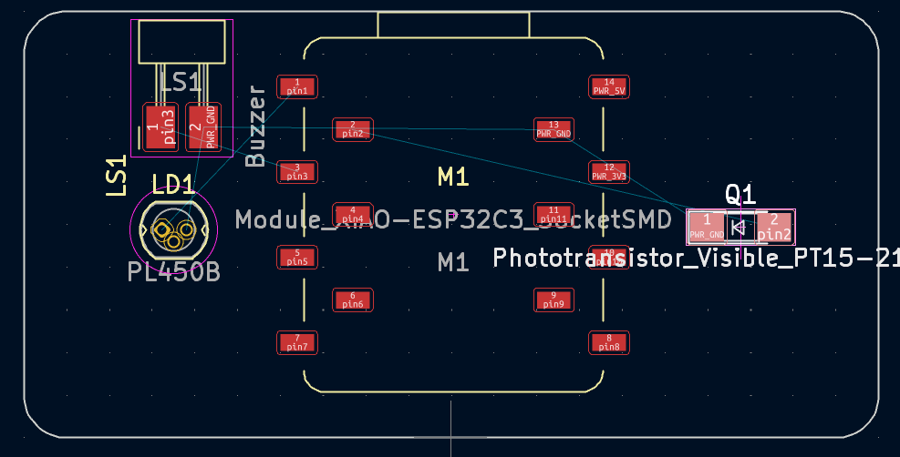
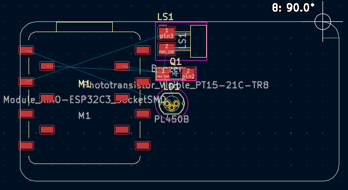
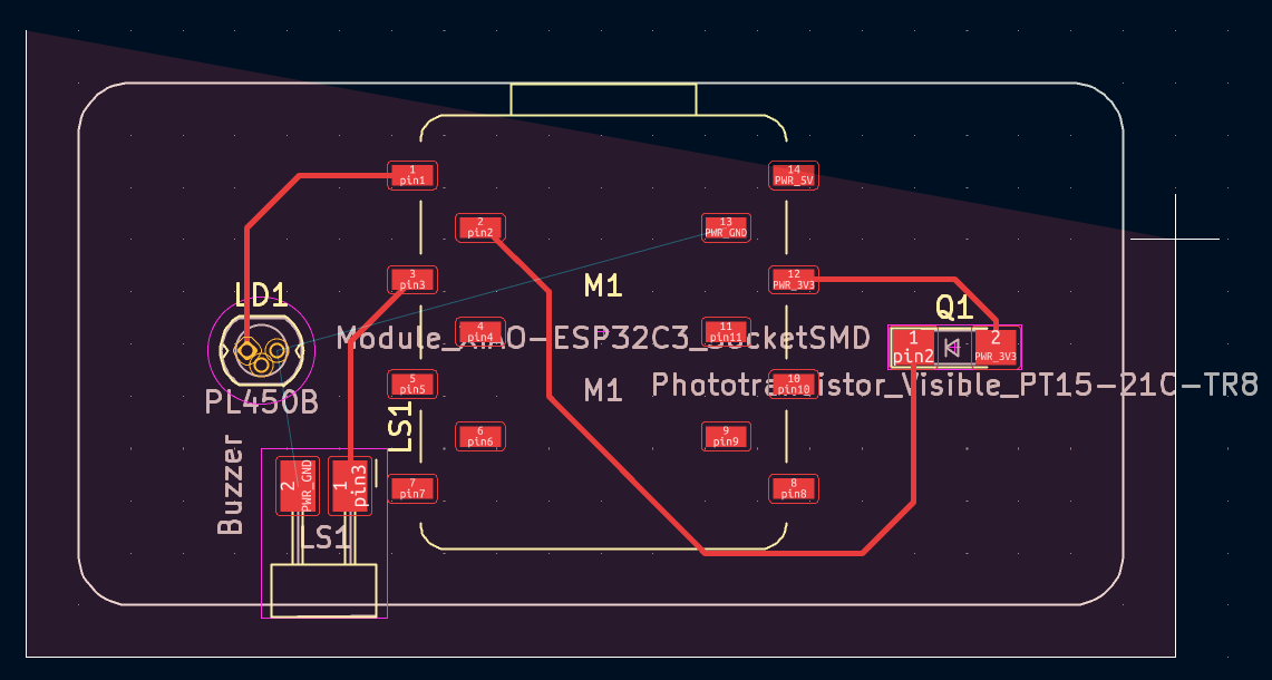
I have placed the microcontroller in the middle, and the laser and detector on the sides. I think as soon as I know the type of the buzzer I will use I can place it in the middle too, as it could face the other direction. For now I just used pin connectors on the side.
Routing tracks
Now comes the actual physical connections of the pins.
At this point I made small edits in the schematic as I realized I am not sure how the components should be used. Regardless, I don't even know if I would use those components so I didn't bother myself with this too much.
While it's possible to autotrace, it's recommended to manually do the tracing. Especially for simple boards like this.
To route tracks make sure the layer is F.Cu as in "front copper" and press X.
Then click on a pin you want to connect.
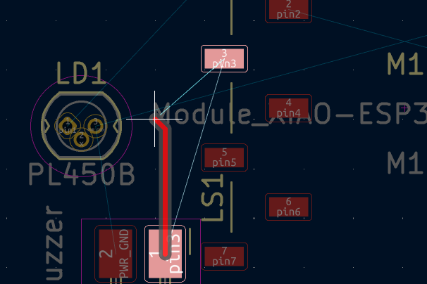
This is like drawing the wiring in the schematic but smarter. As you can see it highlights the pin I am supposed to connect it to.
After connecting all the pins except ground it looks like this:
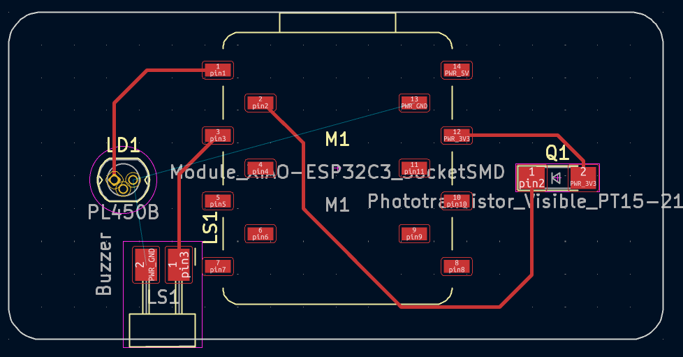
The ground is done a little differently.
Filling ground
First select this tool:
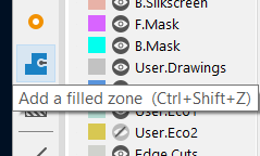
Clicking near the board edge will open this menu:
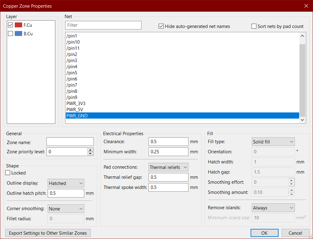
After selecting ground and clicking ok I will draw roughly around the board.
After completing the loop Press B to show/build the filled zone
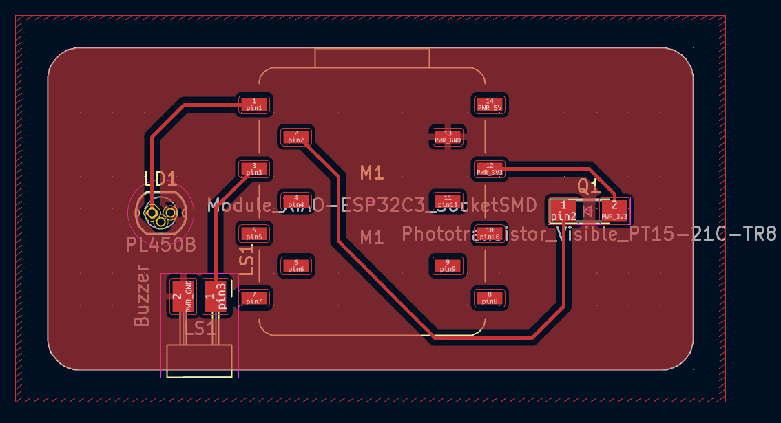
Now the PCB is basically done.
Other tweaks
To edit for example the trace/track width press E
while having the desired parts selected.
Here a great shortcut to select whole track by pressing U
is really helpful.
I changed the track width to 0.4mm
Result
Here is the 3D view of the PCB:
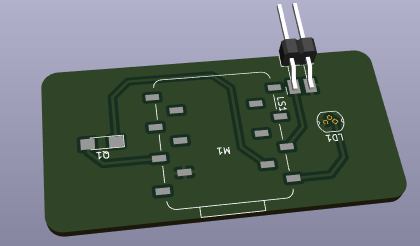
As you can see the footprints I used don't have all the physical representations but that doesn't matter as the connections are still fine.
Source files
I removed the backups from the project folder and zipped it:
Kicad project zipped (31 KB)
End of week 6.