6. Electronics design
Individual project:
Design a development board to interact and communicate with an embedded microcontroller
Extra credit: try another design workflow, make a case for it, simulate its operation.
Group project:
Use the test equipment in your lab to observe the operation of a microcontroller circuit board.
Designing Hello World Board
Designing a “Hello World” board is a great starting point for beginners who want to learn about electronics and embedded systems. Here are the steps to design a “Hello World” board: Identify the components: Create a schematic: Design the PCB:
Also we need EDA (Electronic Design Automation) tools for designing the PCB. Some of them are Autodesk Eagle, KiCad etc.
I have statrted with KiCad.
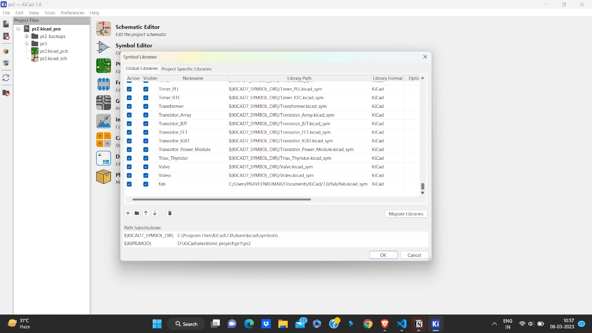
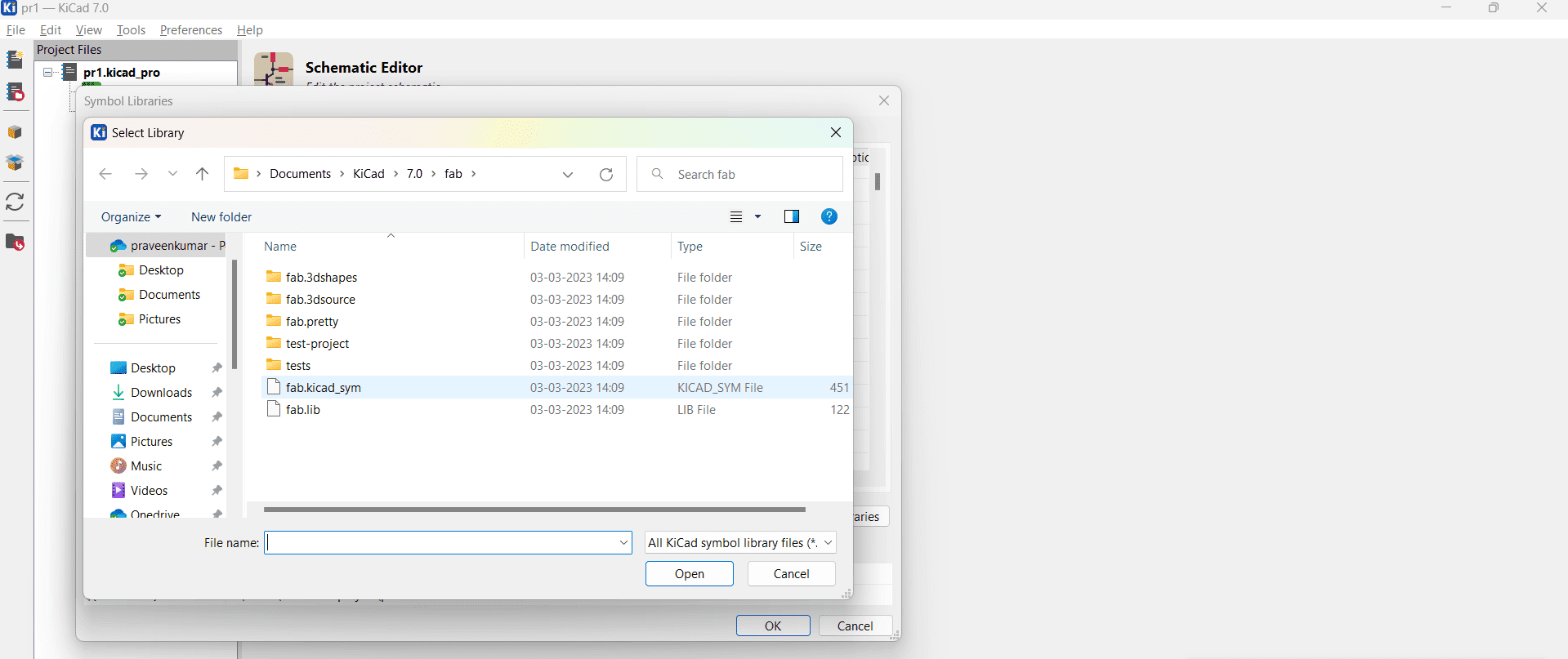
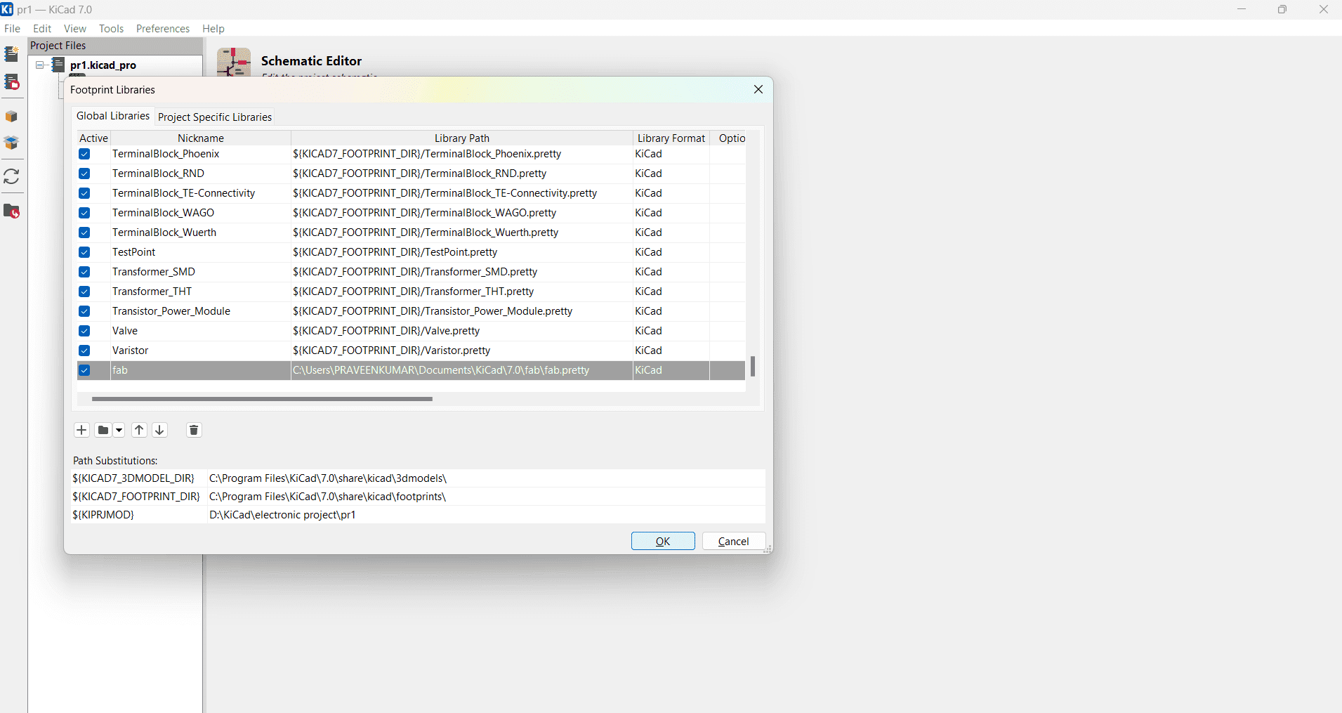
Adding Library
Before staring the design,we have to add libraries of FAB electronic components. For that I followed the installation guide from Git Repository
- First we have to install symbol libraries, for that after opening KiCad, go to “Preference” and select “Manage symbol libraries” and add “fab.kicad_sym”.
- For installing footprint libraries, again go to “preference” and selcet “Mangae Footprint libraries” and add “fab.pretty”.
Starting Designing PCB
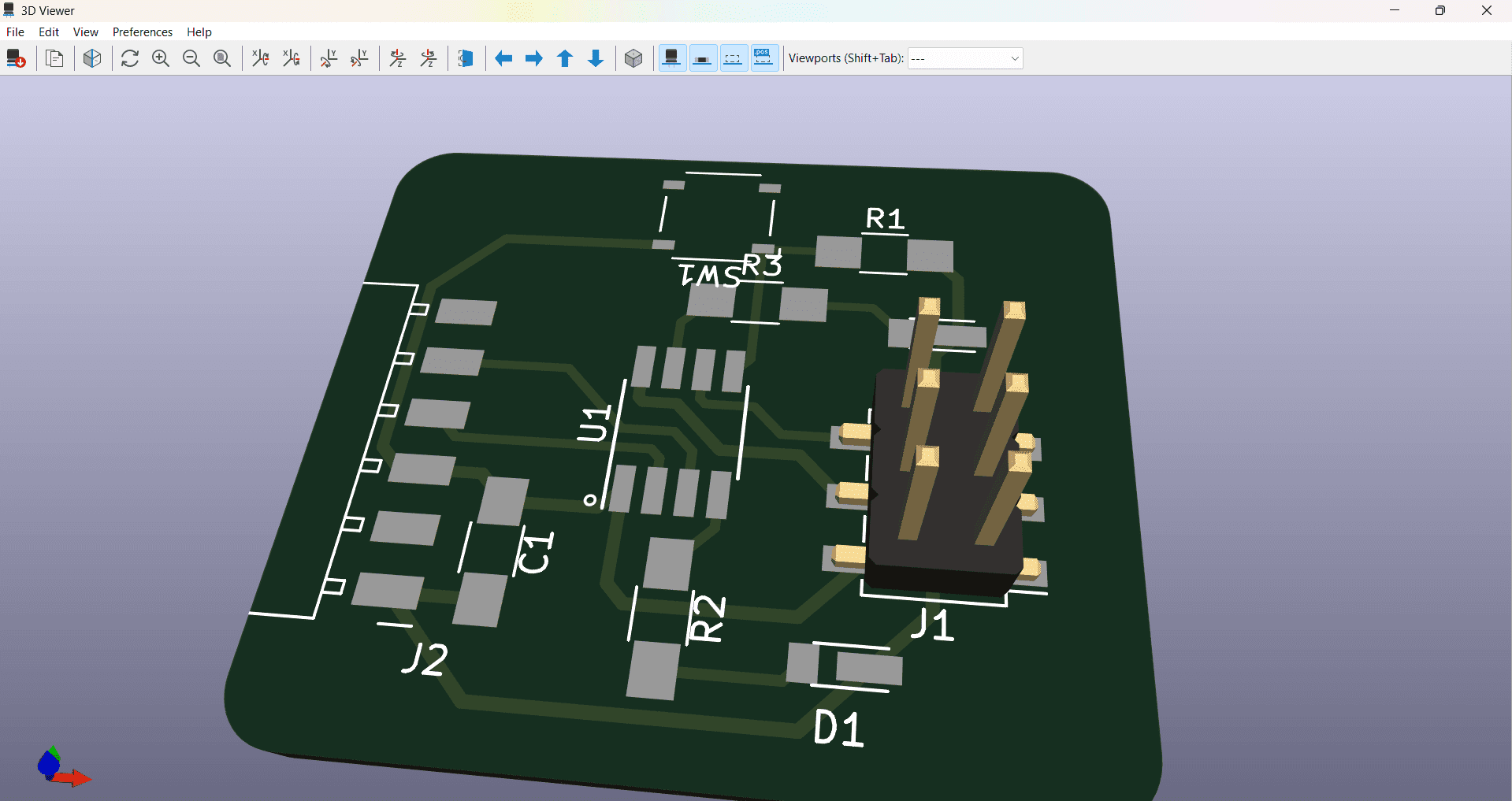
Components Used
-
ATtiny412 SOIC
-
Capacitor 1206
-
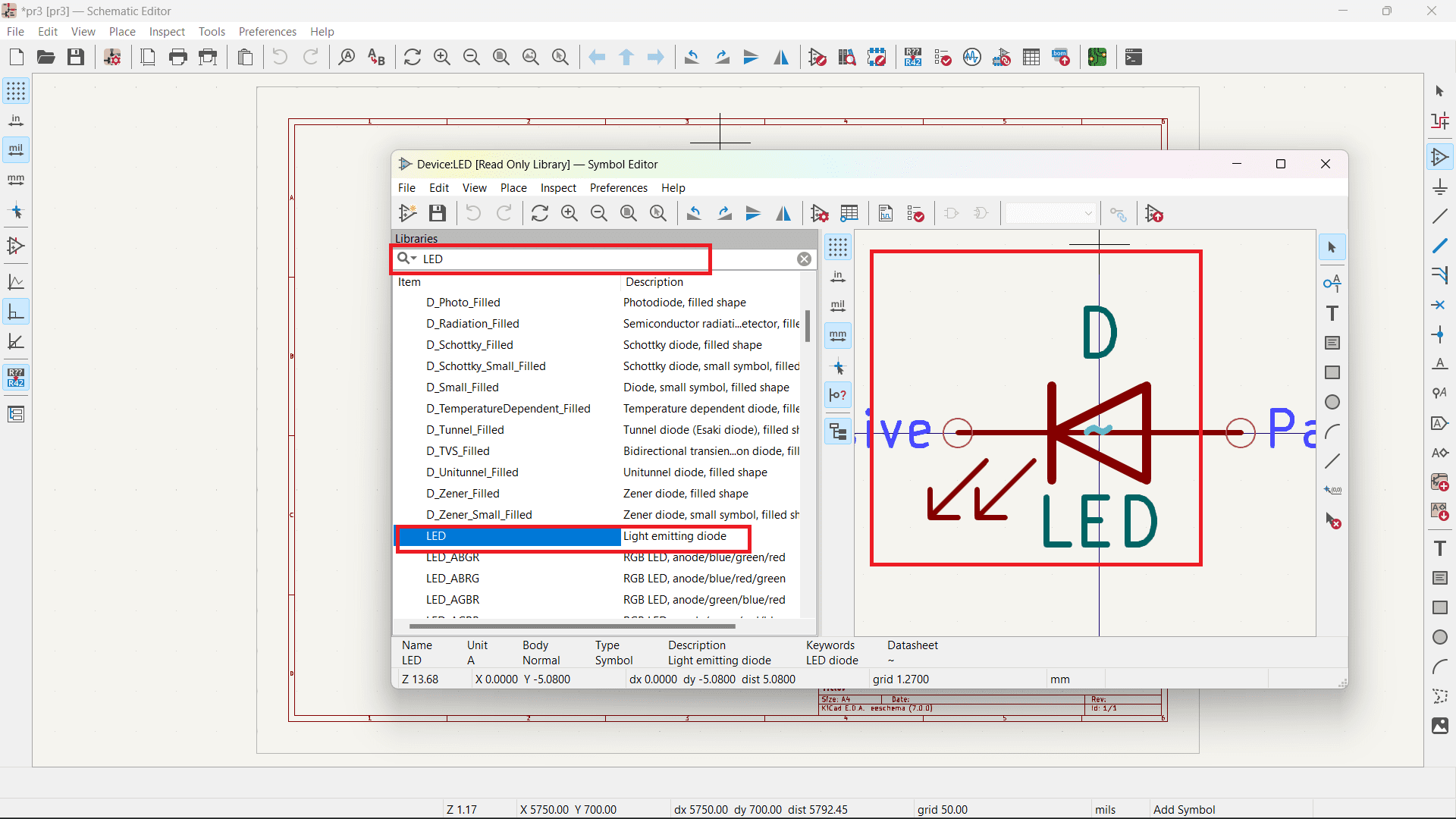
LED_Luminus_1206
-
PinHeader_P2.54mm
-
PinSocket_P2.54mm
-
Resistor_1206
-
Button_ESwitch_4.5x4.5mm
ATtiny412 pin diagram
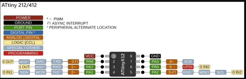
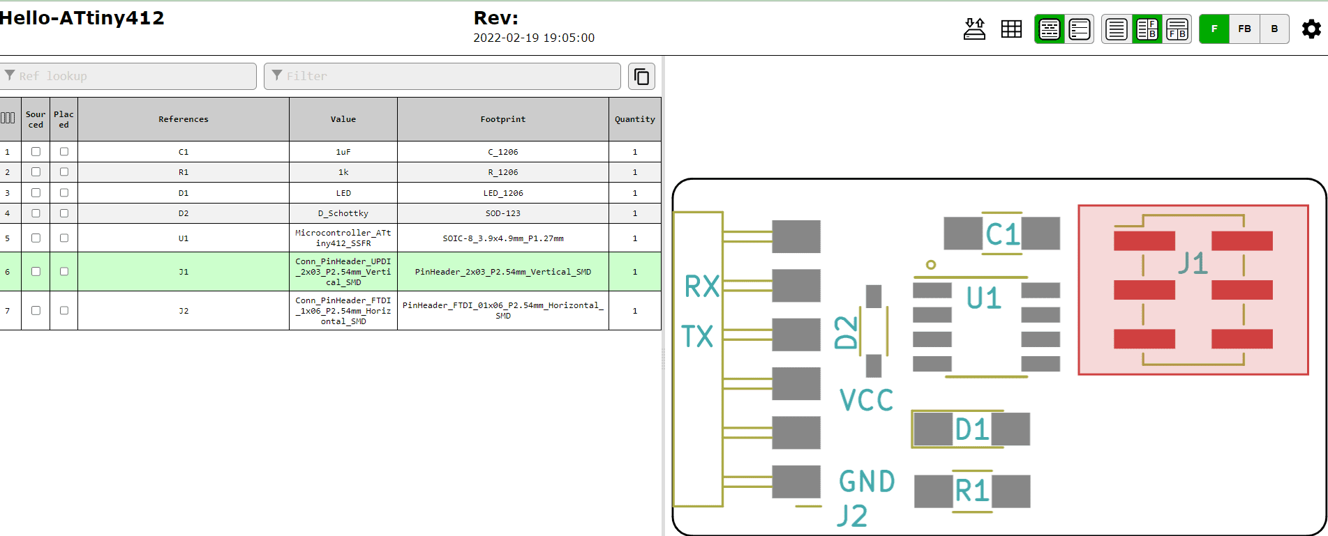
Downloadeď basic hellow board to test UPDI programmer from GitLab fabCloud. From here I collected the BOM. Its shows the resistor was give about 1K. If we put the resistor 1K, the LED brightness will be very low. The current will be only 0.005amp, which can be found out from Ohms law, which states that the current flowing through a resistor is equal to the voltage across the resistor divided by the resistance.In this case, the voltage across the resistor is 5v and the resistance is 1k (1000 ohms). So the current flowing through the circuit is:[code]I = V / R = 5v / 1000 ohms = 0.005 Amp.
Insted of 1K, I am planned to use 499 Ohm, so that enough brightness will possible.
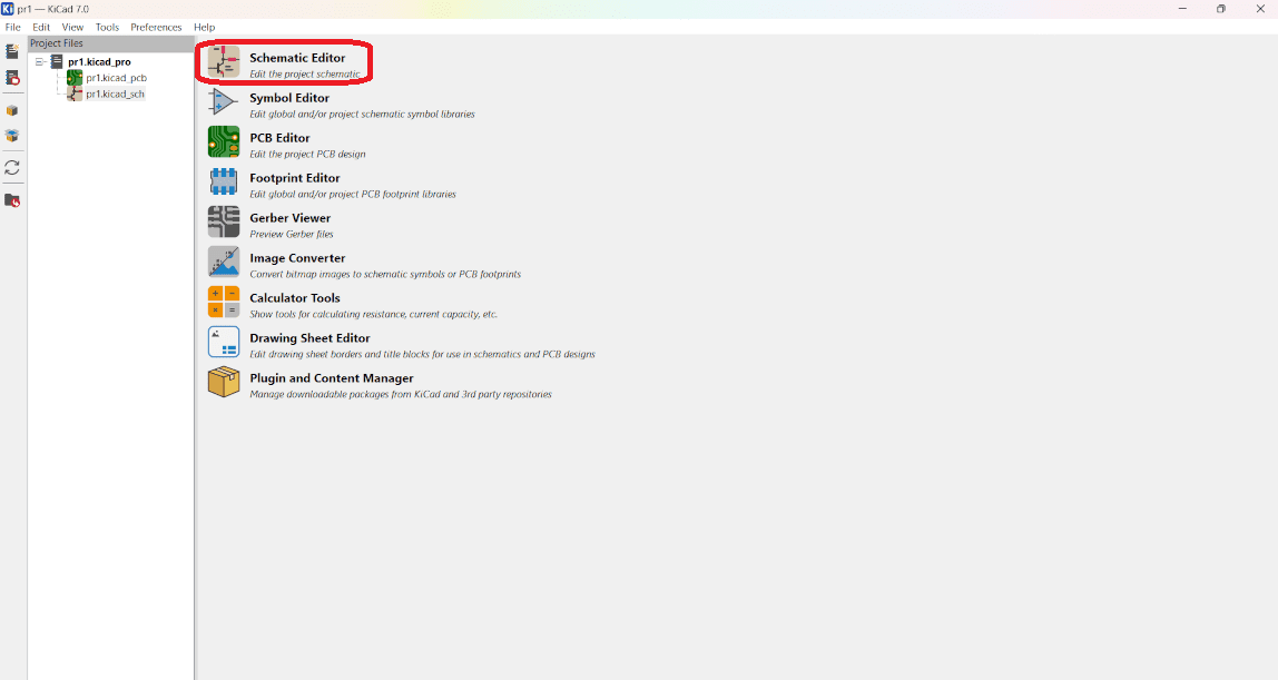
- Desinging the board starts with the schematic editor. Select the schematic editor tab as show below.
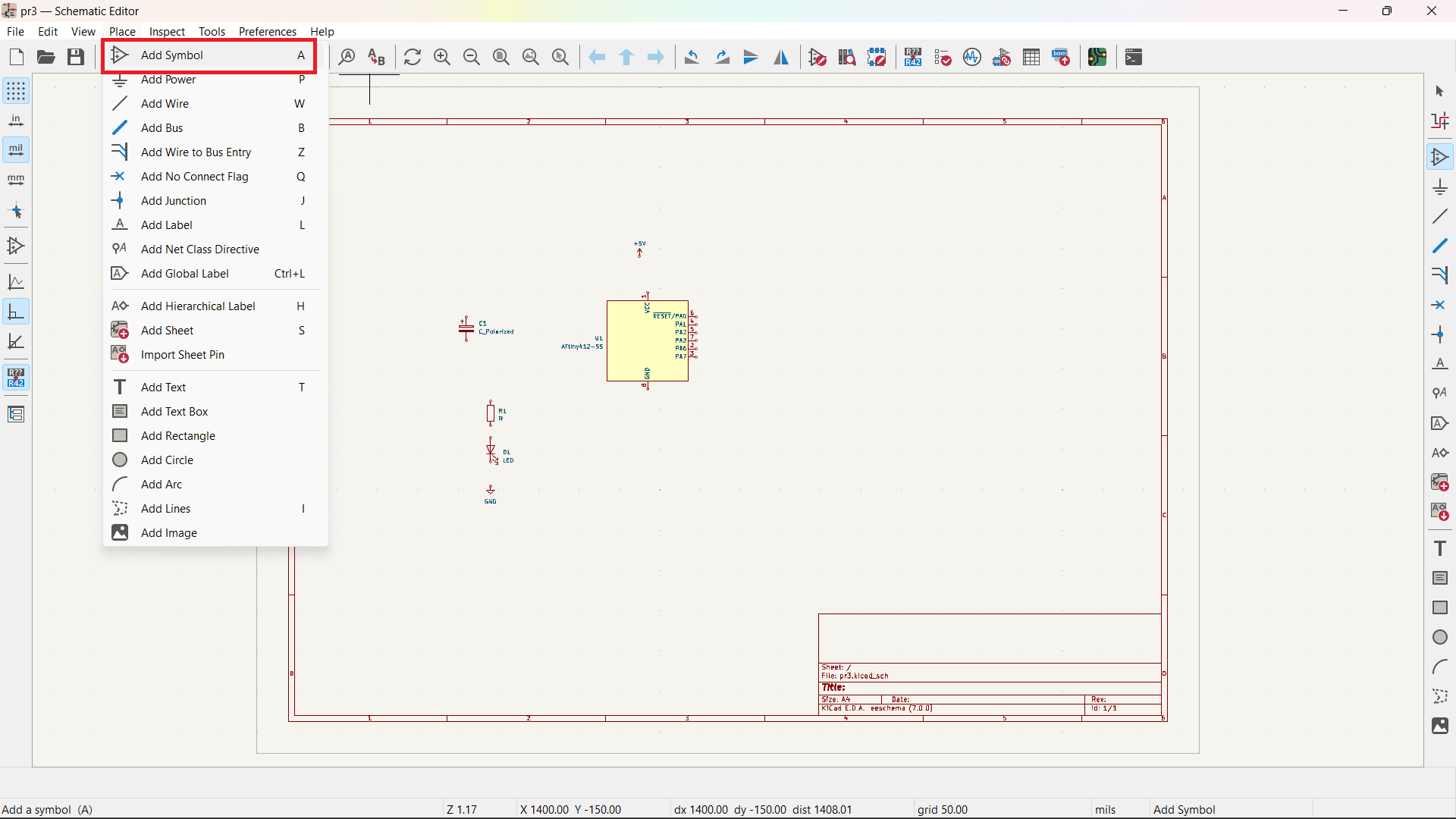
- On a schematic window components can be added by short cut key A. Components can be rorate by R and move by M. Components are added from the library and placed in schematic window.IN my Haloow boar i have selected 1. ATtiny412 SOIC, Capacitor 1206,LED_Luminus_1206,PinHeader_P2.54mm,PinSocket_P2.54mm, Resistor_1206,Button_ESwitch_4.5x4.5mm
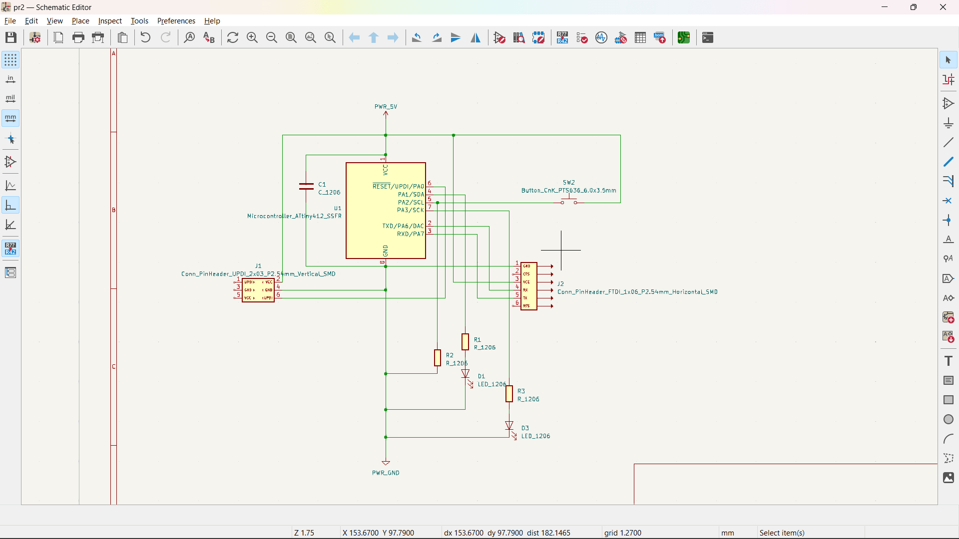
- After adding the components,connection are made as below
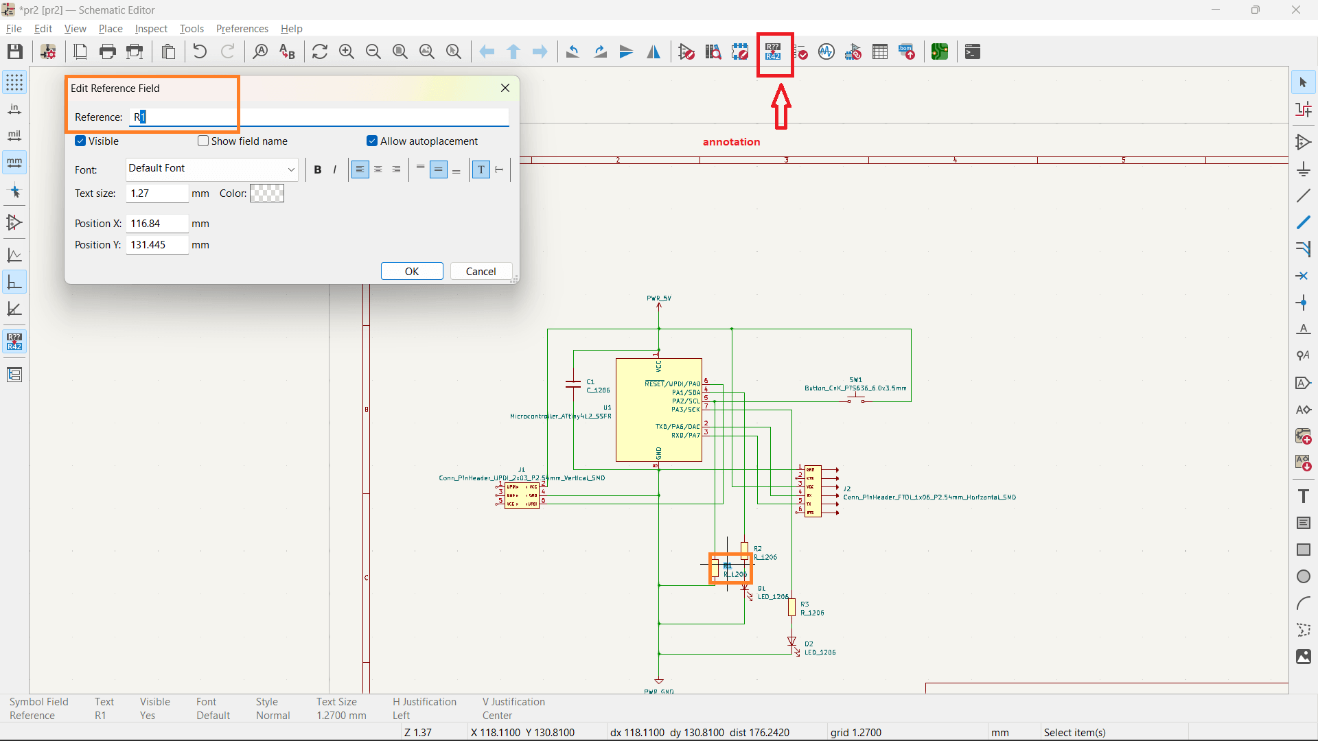
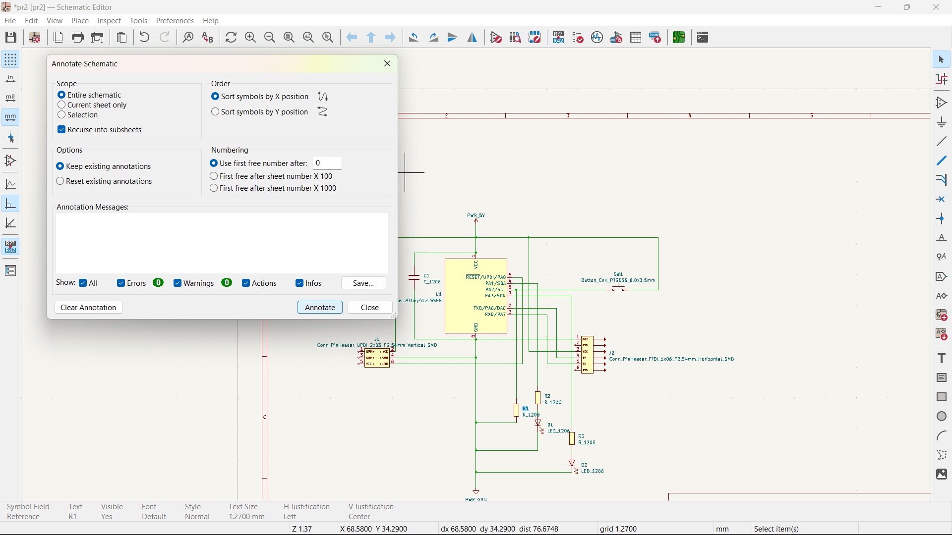
- Now Annotate. One of the many benefits of KiCad is the ability to auto-annotate a schematic. Click on the Annotate schematic components button. Use the default settings and simply click on Annotate button to confirm.In annotation we can edit the name of the componets and give the component its corresponding value. We can edit the references field by double clicking the component text.
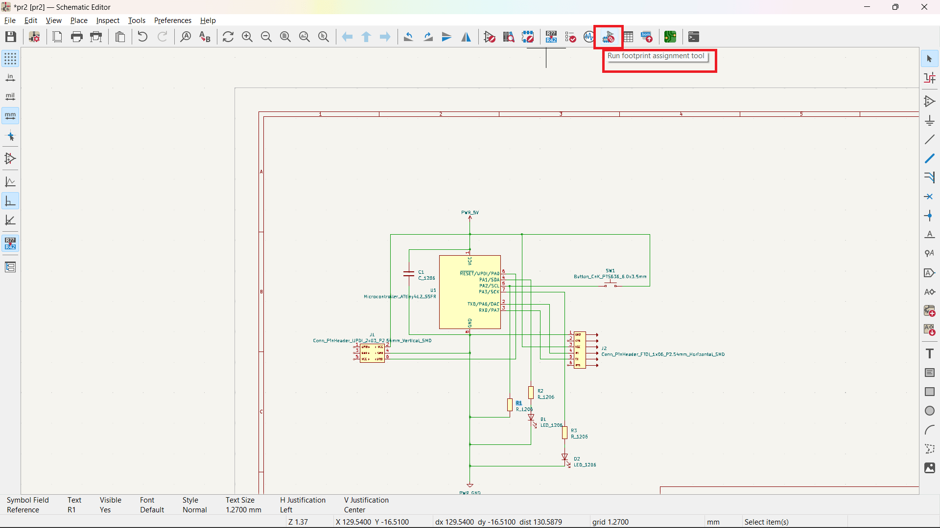
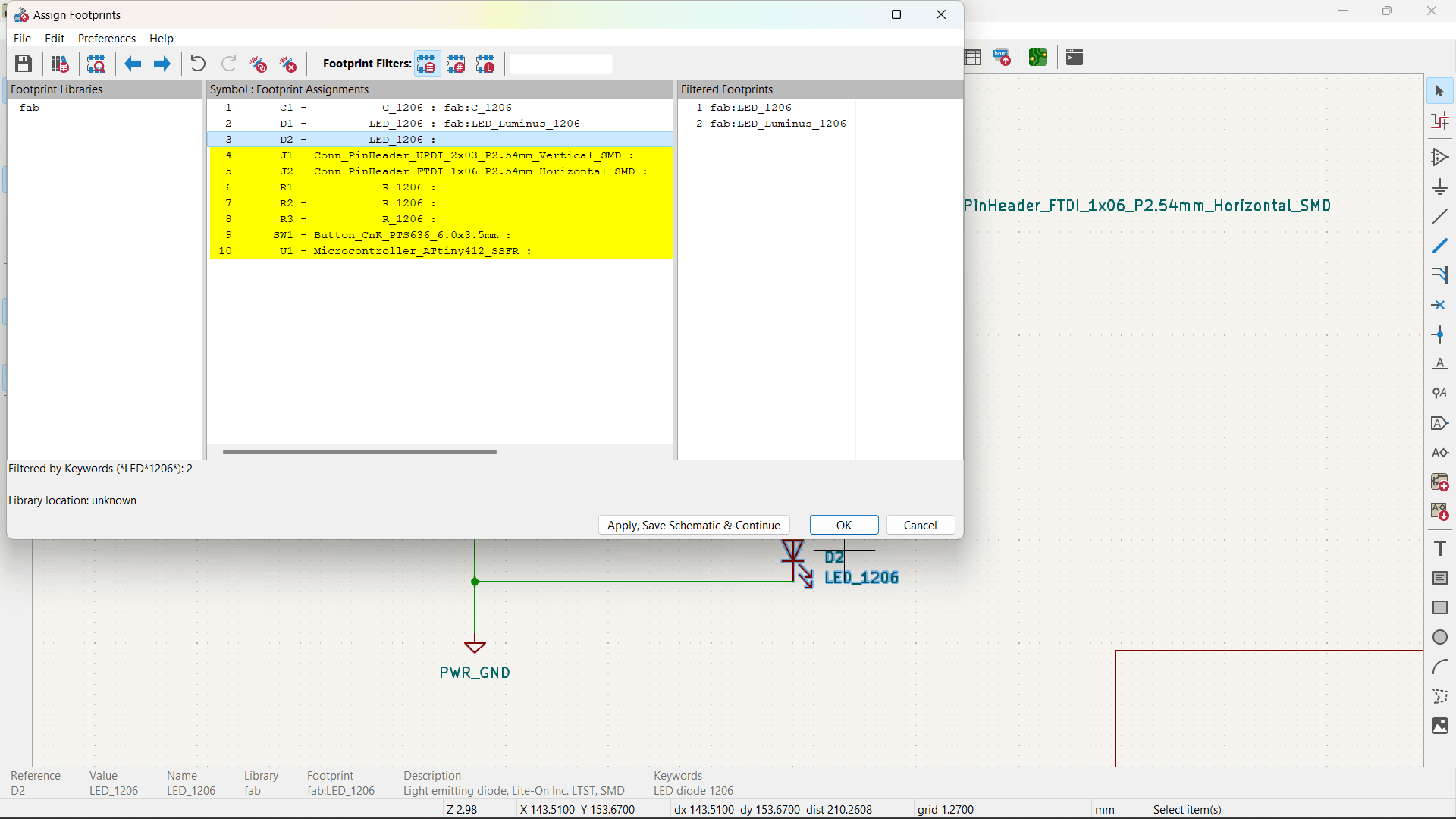
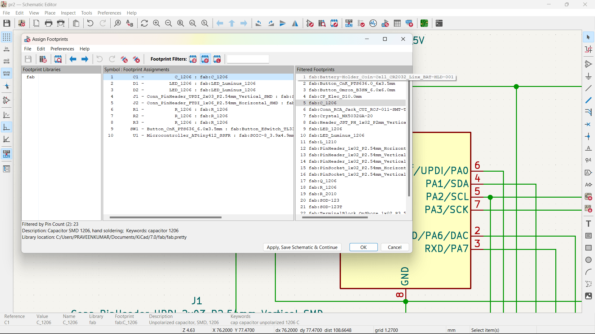
- Now adding the footprints
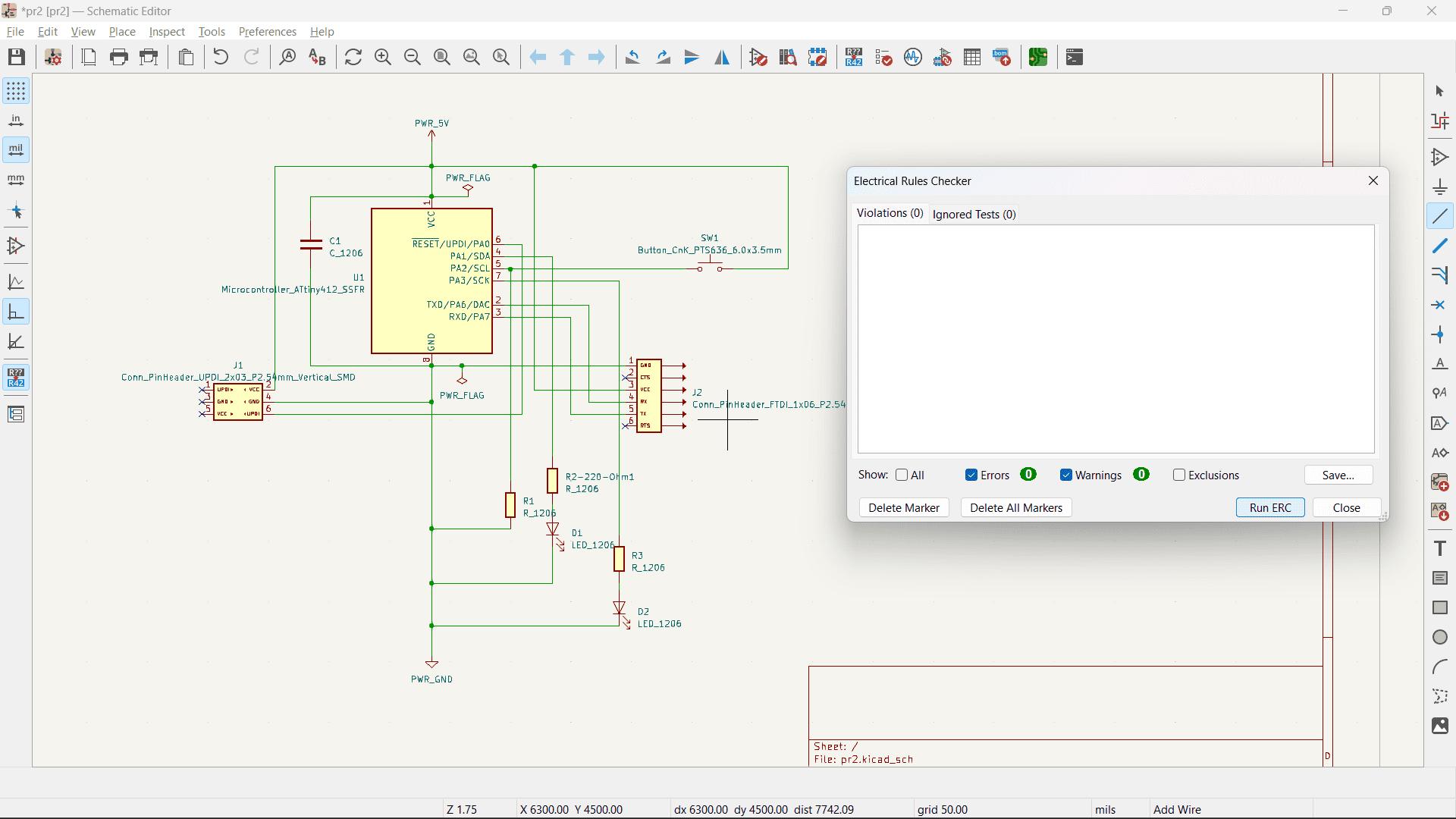
- In electronic board design, ERC (Electrical Rule Checking) involves checking the electrical connectivity of the components on the board and verifying that they meet the required specifications. This includes checking for proper power and signal connections, proper grounding, and any other electrical requirements that need to be met.After all the connections are made,we can check the electrical rules by clicking “inspect and run electrical rules checker”.You will see errors or warning depending on your connection. Initially there were 7 error in my connection. Out of 7, 2 are due to input power pin not driven by any output power pin and the rest are due to the open pin connection which are actualy not required. Here I made a no connection for unconnected pins which reduced the error to 2.
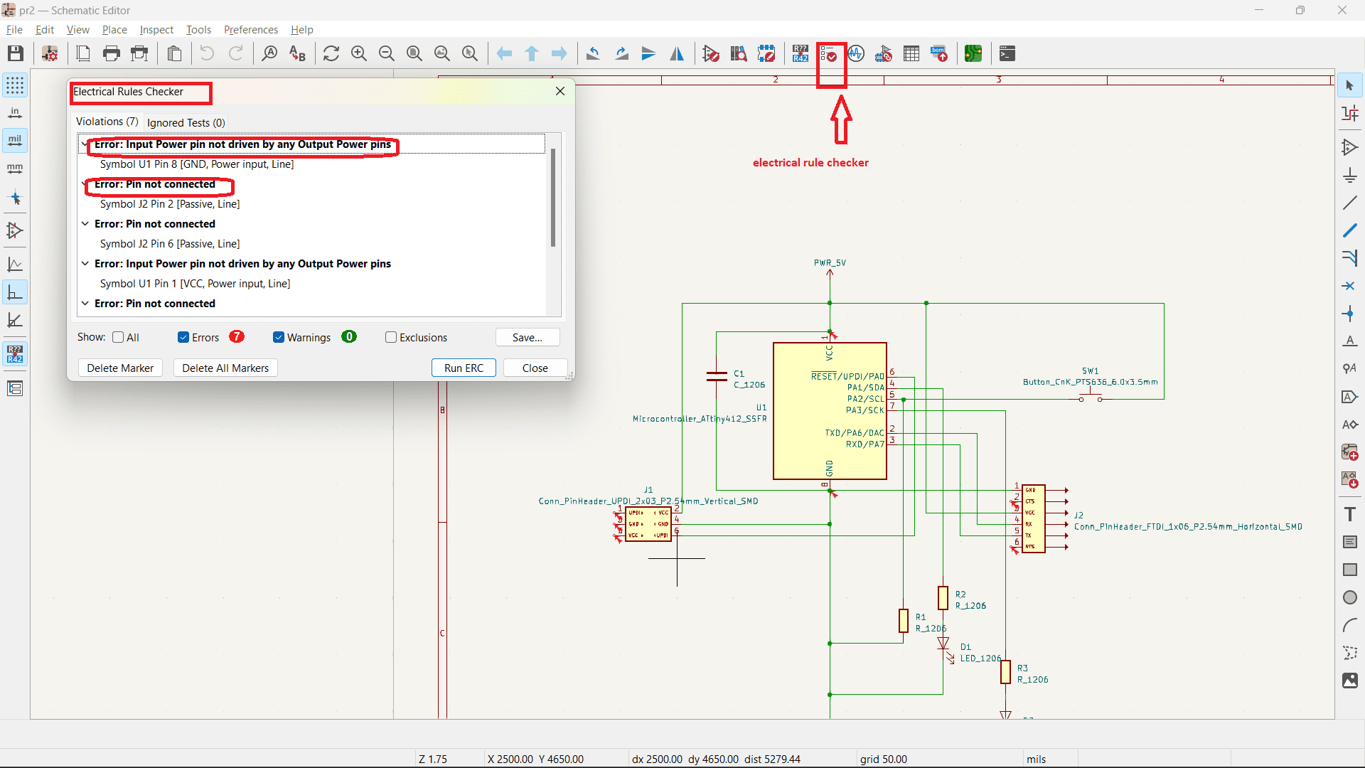
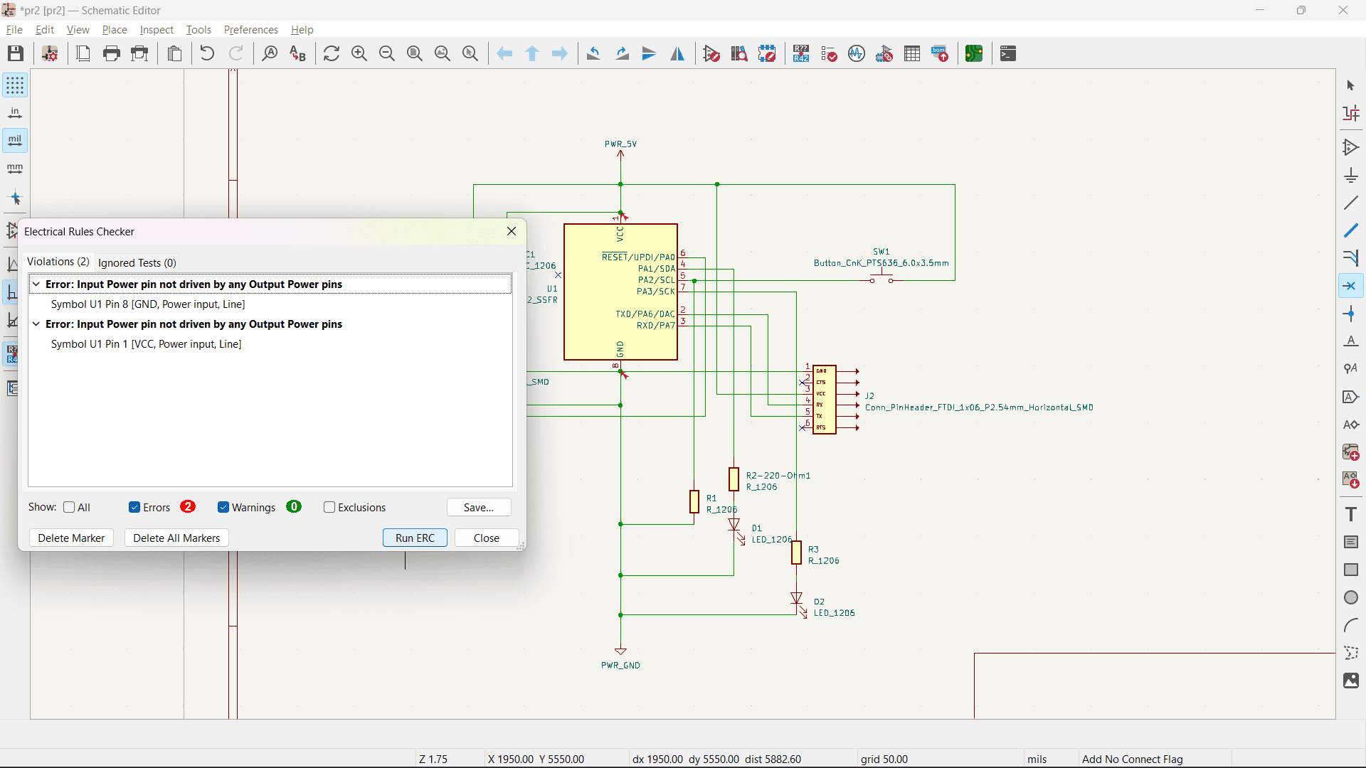
About Input power not driven by any Output power pins,I added power flag from library and it worked.
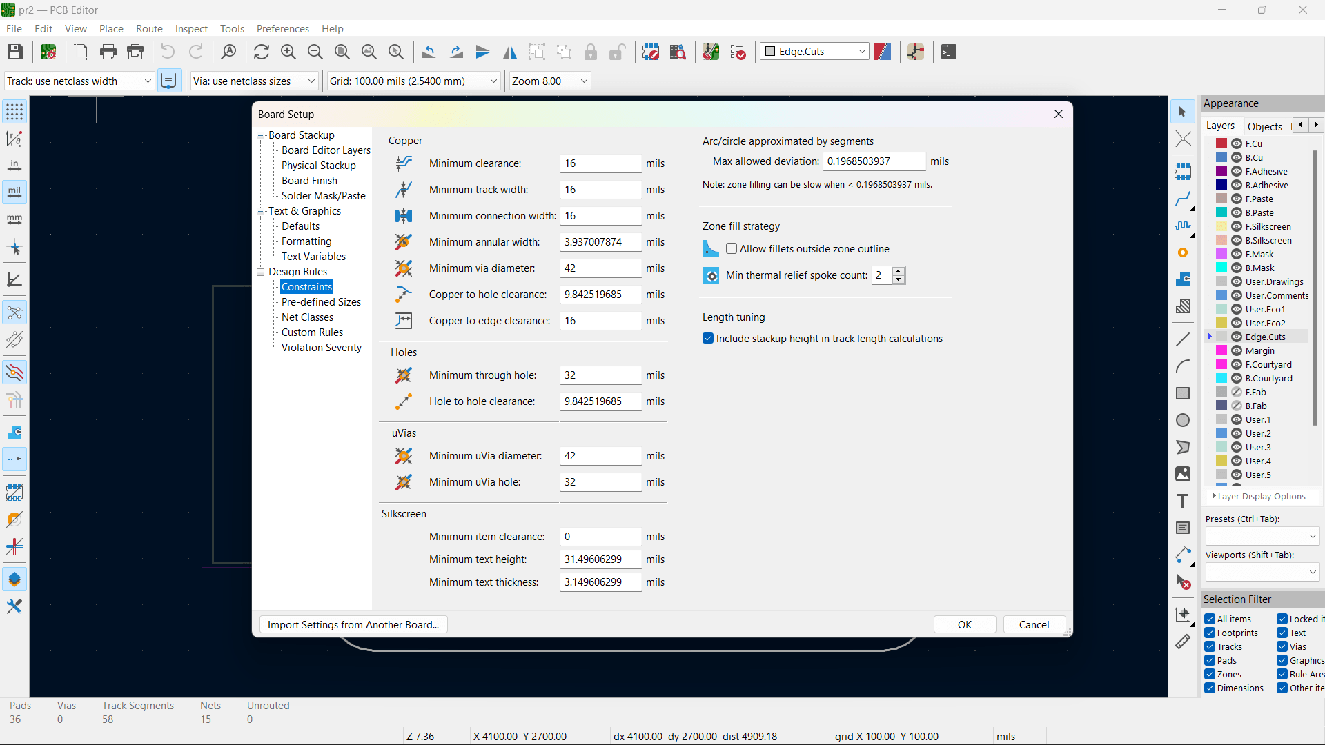
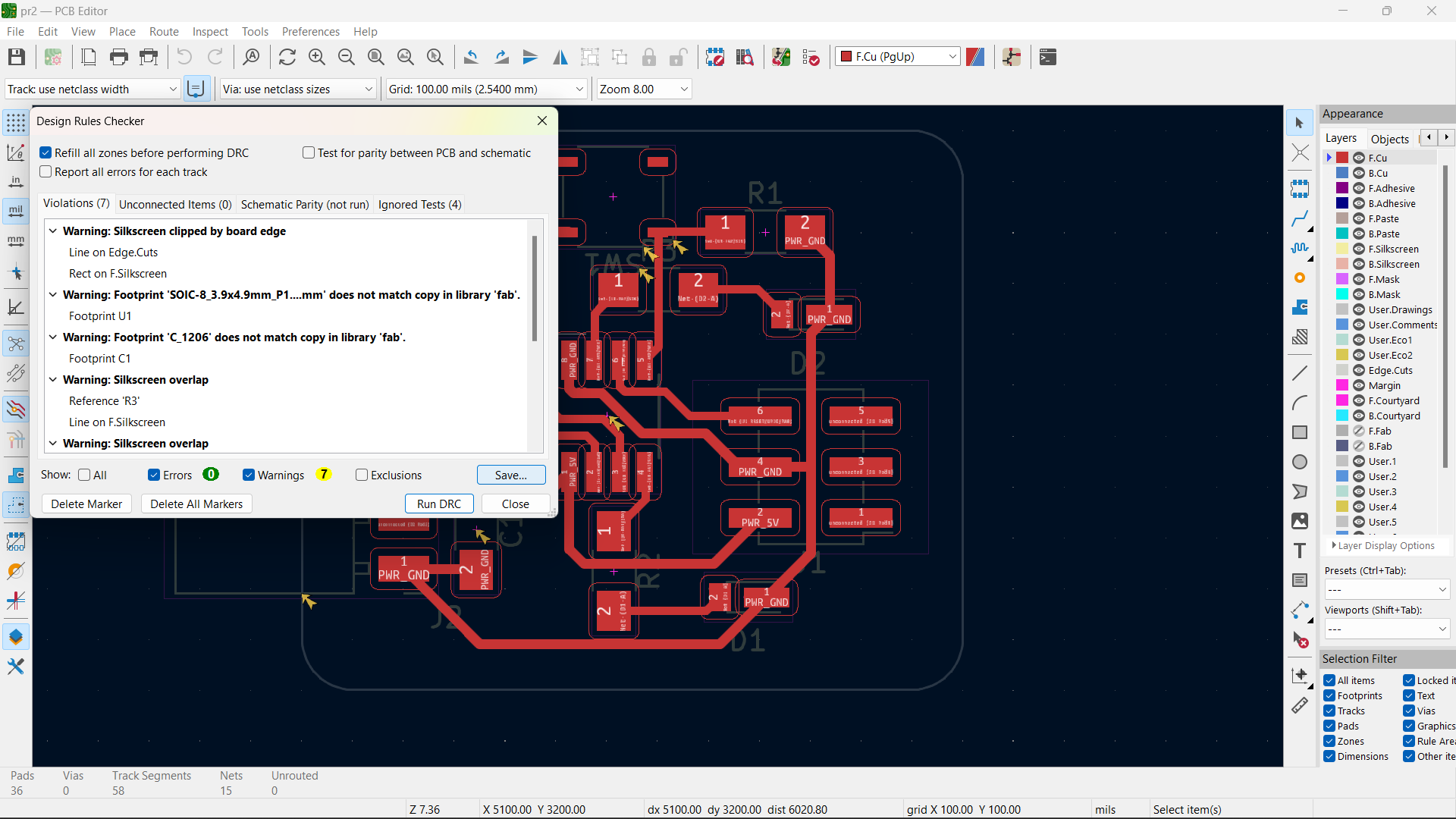
Till here all the process in Schematic Editor are over and now its time to go to PCB Editor. Before going in to PCB editor, Design rule have to be set as below.DRC (Design Rule Checking) used to ensure the quality and functionality of the final product.DRC, involves checking the physical layout of the board to ensure that it conforms to the manufacturing constraints and requirements of the design. This includes checking for proper spacing between components, proper alignment of through-holes and vias, and compliance with other physical layout requirements. In my case there was no error. Hence I proceded further.
The values I used here is as per the instruction from my instructor, since I am using this field for the first time.
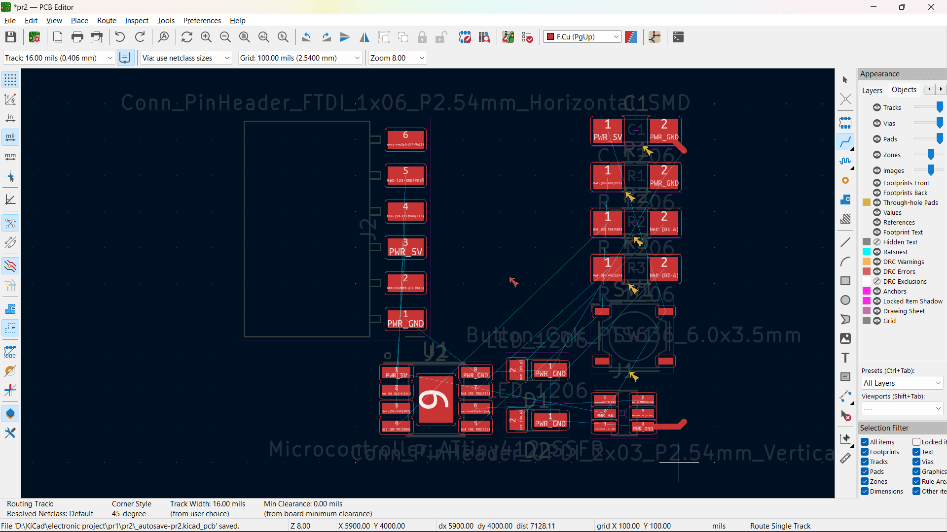
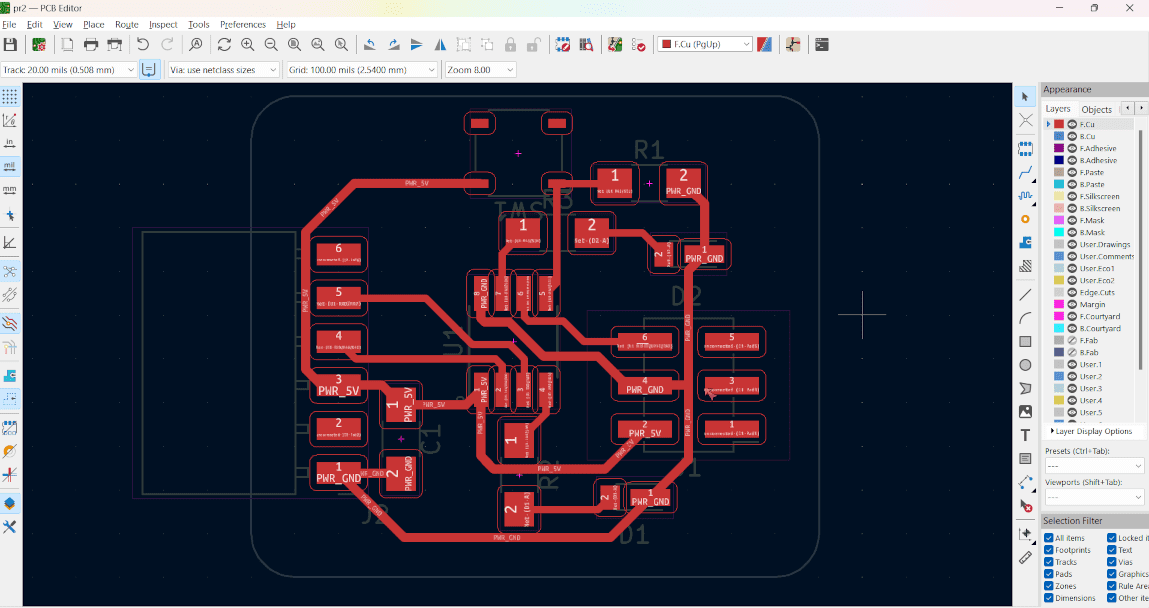
- Updating Schematic to PCB Editor
Click Tools, then choose Update PCB from Schematic. To arrange the components and create a circuit board design, the PCB layout editor uses the move and rotate commands. In my situation, I choose to go with a straightforward square shape. Now build the connecting tracks between the parts using route tracks.
Final 3D view of my circut