9. Embedded programming
Group Assignment
Compare the performance and development workflows for other architectures
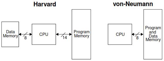
HARVARD: This architecture has program memory and data memory as separate memories and are accessed from separate buses.
VON-NEUMANN: The traditional von Neumann architecture has the program and the data in the same memory bank and is obtained using the same bus.
CISC: Complex Instruction Set Computing
RISC: Reduced Instruction Set Computing
AVR: Advanced Virtual RISC
ARM: Advanced RISC Machines and originally Acorn RISC Machine
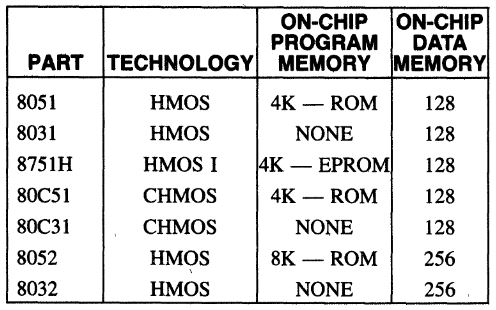
Intel Microcontroller - MCS®-51 Family Members
The major features are:
• 8 Bit CPU
• On Chip oscillator and clock circuitry
• 32 I/O lines
• 110 Intructions
• 64K address space for external data memory
• 64K address space for external program memory
• Two 16 bit timer/counters (three on 8032/8052)
• A five source interrupt structure (six sources on 8032/8052) with two priority levels
• Full duplex serial port
• Boolean processor
Family devices
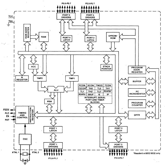
Architectural Block Diagram
This microcontroller family has HARVARD arquitecture with CISC.
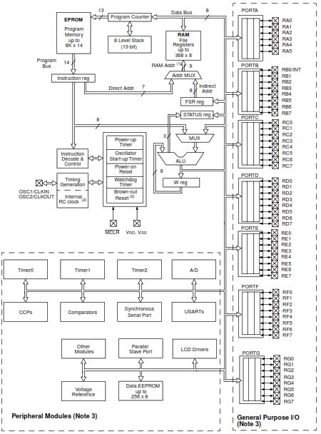
Microchip Microcontroller - PICmicro 16F87XA MCU Family
The major features are:
• Only 35 single-word instructions to learn
• All single-cycle instructions except for program branches, which are two-cycle
• Operating speed: DC – 20 MHz clock input
DC – 200 ns instruction cycle
• Up to 8K x 14 words of Flash Program Memory,
Up to 368 x 8 bytes of Data Memory (RAM),
Up to 256 x 8 bytes of EEPROM Data Memory
• Pinout compatible to other 28-pin or 40/44-pin PIC16CXXX and PIC16FXXX microcontrollers
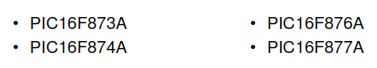
Family devices
Architectural Block Diagram
This microcontroller family has HARVARD arquitecture with RISC.
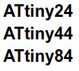
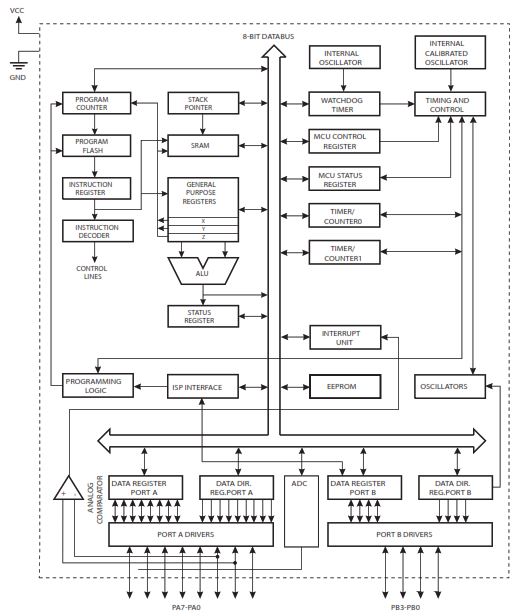
ATMEL Microcontroller - AVR ATtiny 24-44-84 & ATmega 48PA-88PA-168PA-328P
ATtiny, the major features are:
- High Performance, Low Power AVR® 8-Bit Microcontroller
- Advanced RISC Architecture
– 120 Powerful Instructions – Most Single Clock Cycle Execution
– 32 x 8 General Purpose Working Registers
– Fully Static Operation - Non-Volatile Program and Data Memories
– 2/4/8K Bytes of In-System Programmable Program Memory Flash
• Endurance: 10,000 Write/Erase Cycles
– 128/256/512 Bytes of In-System Programmable EEPROM
• Endurance: 100,000 Write/Erase Cycles
– 128/256/512 Bytes of Internal SRAM
– Data Retention: 20 years at 85°C / 100 years at 25°C
– Programming Lock for Self-Programming Flash & EEPROM Data Security
Family devices
Architectural Block Diagram
This microcontroller family has HARVARD arquitecture based on AVR enhanced RISC.
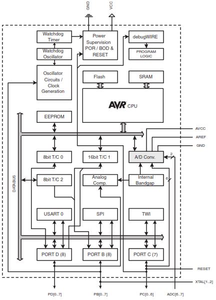
ATmega, the major features are:
- High Performance, Low Power AVR® 8-Bit Microcontroller
- Advanced RISC Architecture
– 131 Powerful Instructions – Most Single Clock Cycle Execution
– 32 x 8 General Purpose Working Registers
– Fully Static Operation
– Up to 20 MIPS Throughput at 20 MHz
– On-chip 2-cycle Multiplier - High Endurance Non-volatile Memory Segments
– 4/8/16/32K Bytes of In-System Self-Programmable Flash progam memory (ATmega48PA/88PA/168PA/328P)
– 256/512/512/1K Bytes EEPROM (ATmega48PA/88PA/168PA/328P)
– 512/1K/1K/2K Bytes Internal SRAM (ATmega48PA/88PA/168PA/328P)
– Write/Erase Cycles: 10,000 Flash/100,000 EEPROM
– Data retention: 20 years at 85°C/100 years at 25°C
– Optional Boot Code Section with Independent Lock Bits
In-System Programming by On-chip Boot Program
True Read-While-Write Operation
– Programming Lock for Software Security
Family devices

Architectural Block Diagram
This microcontroller family has HARVARD arquitecture based on AVR enhanced RISC.
Main Difference between AVR, ARM, 8051 and PIC Microcontrollers
|
8051 |
PIC |
AVR |
ARM |
|
|
Bus width |
8-bit for standard core | 8/16/32-bit | 8/32-bit | 32-bit mostly also available in 64-bit |
|
Communication Protocols |
UART, USART,SPI,I2C | PIC, UART, USART, LIN, CAN, Ethernet, SPI, I2S | UART, USART, SPI, I2C, (special purpose AVR support CAN, USB, Ethernet) |
UART, USART, LIN, I2C, SPI, CAN, USB, Ethernet, I2S, DSP, SAI (serial audio interface), IrDA |
|
Speed |
12 Clock/instruction cycle | 4 Clock/instruction cycle | 1 clock/ instruction cycle | 1 clock/ instruction cycle |
|
Memory |
ROM, SRAM, FLASH | SRAM, FLASH | Flash, SRAM, EEPROM | Flash, SDRAM, EEPROM |
|
ISA |
CLSC |
Some feature of RISC |
RISC | RISC |
|
Memory Architecture |
Harvard architecture with CISC | Harvard architecture with RISC | Harvard arquitecture based on AVR enhanced RISC | Harvard arquitecture based on ARM enhanced RISC |
|
Power Consumption |
Average | Low | Low | Low |
|
Families |
8051 variants | PIC16,PIC17, PIC18, PIC24, PIC32 | Tiny, Atmega, Xmega, special purpose AVR | ARMv4,5,6,7 and series |
|
Community |
Vast | Very Good | Very Good | Vast |
|
Manufacturer |
NXP, Atmel, Silicon Labs, Dallas, Cyprus, Infineon, etc. | Microchip Average | Atmel | Apple, Nvidia, Qualcomm, Samsung Electronics, and TI etc. |
| Cost (as compared to features provide) | Very Low | Average | Average | Low |
|
Other Feature |
Known for its Standard | Cheap | Cheap, effective | High speed operation
Vast
|
|
Popular Microcontrollers |
AT89C51, P89v51, etc. | PIC18fXX8, PIC16f88X, PIC32MXX | Atmega8, 16, 32, Arduino Community | LPC2148, ARM Cortex-M0 to ARM Cortex-M7, etc. |
ESP32-XX Family
The ESP32 is a dual-core system with two Harvard Architecture Xtensa LX6 CPUs. All embedded memory, external memory and peripherals are located on the data bus and/or the instruction bus of these CPUs.
With some minor exceptions, the address mapping of two CPUs is symmetric, meaning that they use the same addresses to access the same memory. Multiple peripherals in the system can access embedded memory via DMA.
The two CPUs are named “PRO_CPU” and “APP_CPU” (for “protocol” and “application”), however, for most purposes the two CPUs are interchangeable.
The major features are:
- Address Space
– Symmetric address mapping
– 4 GB (32-bit) address space for both data bus and instruction bus
– 1296 KB embedded memory address space
– 19704 KB external memory address space
– 512 KB peripheral address space
– Some embedded and external memory regions can be accessed by either data bus or instruction bus
– 328 KB DMA address space
- Embedded Memory
– 448 KB Internal ROM
– 520 KB Internal SRAM
– 8 KB RTC FAST Memory
– 8 KB RTC SLOW Memory
- External Memory
Off-chip SPI memory can be mapped into the available address space as external memory. Parts of the embedded memory can be used as transparent cache for this external memory.
– Supports up to 16 MB off-Chip SPI Flash.
– Supports up to 8 MB off-Chip SPI SRAM.
- Peripherals
– 41 peripherals
- DMA
– 13 modules are capable of DMA operation
Family devices
ESP01, ESP01s, ESP-12E (NodeMCU, Wenos) and so on.
Architectural Block Diagram
The ESP32 is a dual-core system with two Harvard Architecture Xtensa LX6 CPUs.
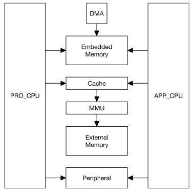
System Structure
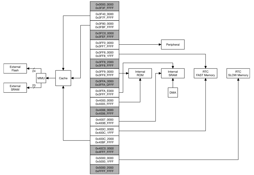
System Address Mapping
Programming the NodeMCU with Arduino IDE
First, we configure Arduino IDE
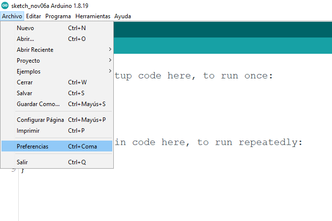
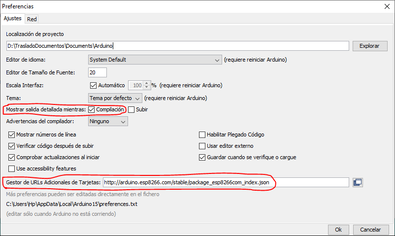
Go to the preferences menu
In the “Additional Card URLs Manager” box we add: http://arduino.esp8266.com/stable/package_esp8266com_index.json
Add url card
Then we go to Tools>board: …>Card Manager
And we look in the list “esp8266 by ESP8266 Community“, we select it and install
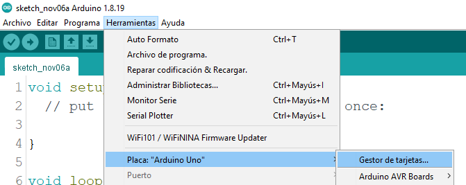
Go to the board menu
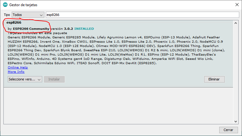
Esp8266 by ESP8266 Community
The installation will take a while, at the end, the ESP8266 item should mark them as installed.
Now in tools>>>boards, the new board should be installed.
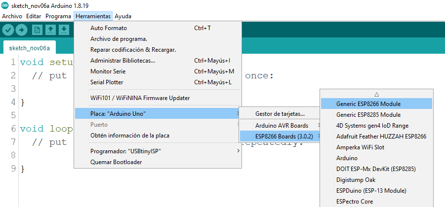
We select “Generic esp8266 module”
Programming another microcontroller, NodeMCU-32 based on the ESP32
Individual Assignment
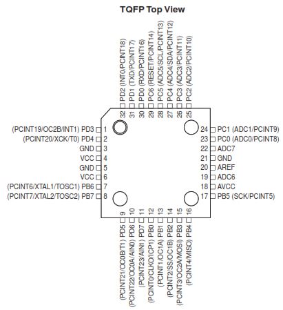
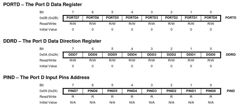
Reading the data sheet of the ATmega328p
Pin configutation
Port D configuration, reading and writing registers
Use your programmer to program your board to do something
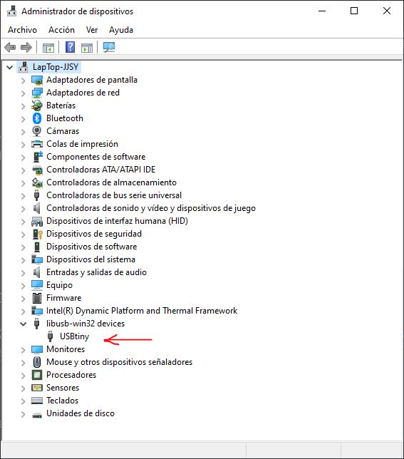
We check the recognition of our programmer in windows.
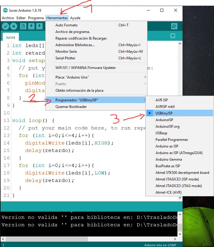
In Arduino IDE we select the type of programmer, it is programmer USBtinyISP programmer.
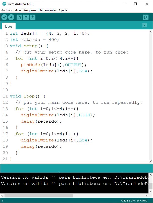
We created our program, it is a light sequence.
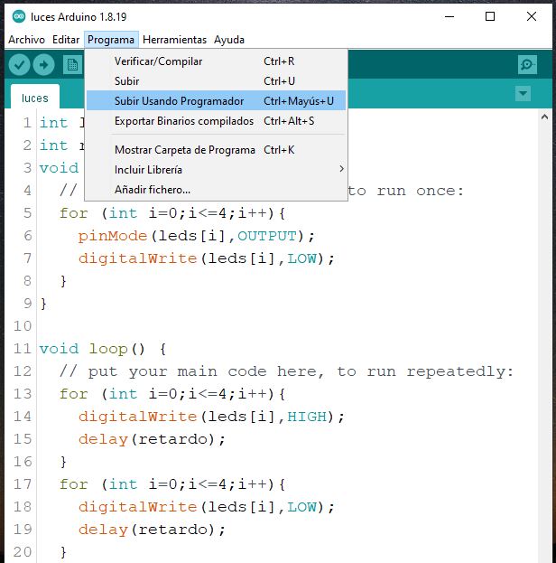
In program menu, we selected the option “upload using programmer”
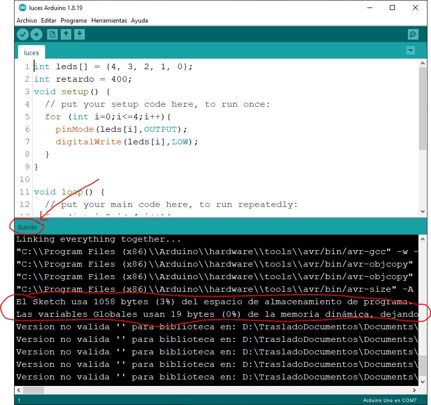
We verify the programming by confirming the messages “upload”.
Program code
int leds[] = {4, 3, 2, 1, 0};
int retardo = 400;
void setup() {
  // put your setup code here, to run once:
  for (int i=0;i<=4;i++){
    pinMode(leds[i],OUTPUT);
    digitalWrite(leds[i],LOW);
  }
}

void loop() {
  // put your main code here, to run repeatedly:
  for (int i=0;i<=4;i++){
    digitalWrite(leds[i],HIGH);
    delay(retardo);
  }
  for (int i=0;i<=4;i++){
    digitalWrite(leds[i],LOW);
    delay(retardo);
  }
}
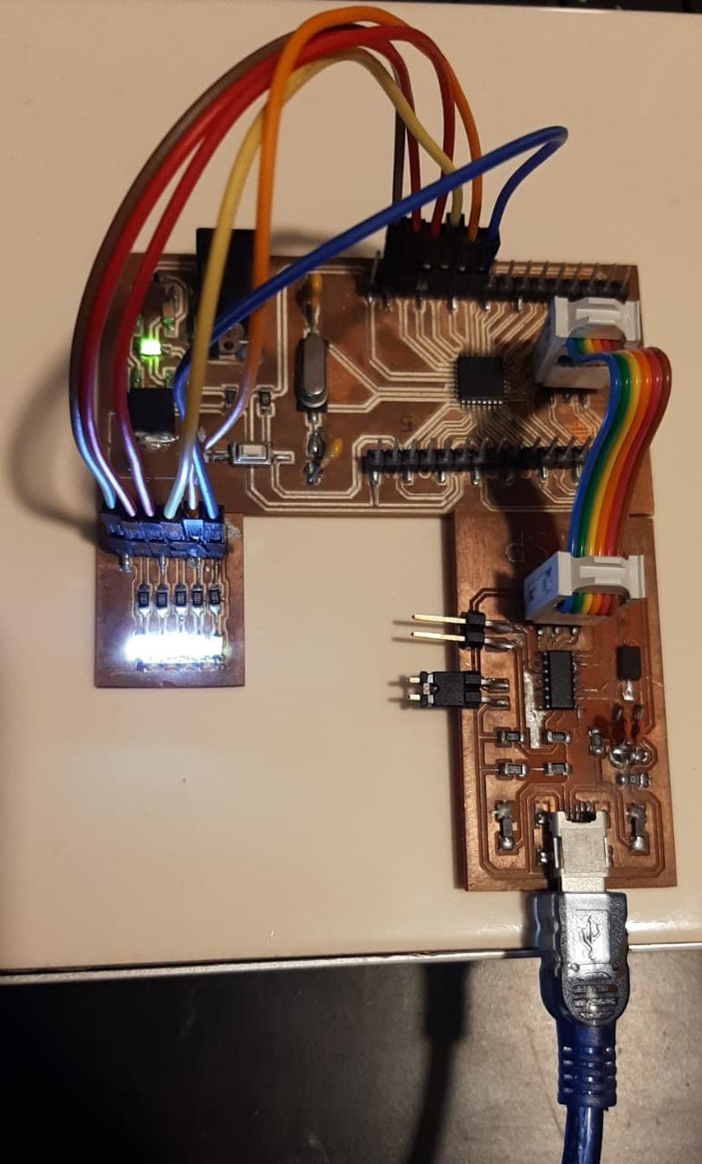
My complete circuit, ATmega328p board, fabISP programmer and LEDs board.
Programming my ATmega3280p board with my fabISP programmer.