5. Electronics production
Group assignment:
Characterize the design rules for your in-house PCB production process
In this activity it is important to carry out engraving tests with the drill bits that are available, this will allow us to know the track and engraving thicknesses that we can carry out in our plate designs. For them we made the following design:
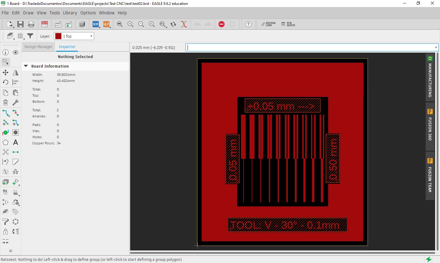
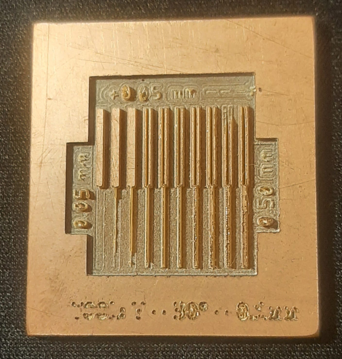
I designed my own layer test PCB, this PCB shows track width and groove width ranging from 0.05mm to 0.50mm.
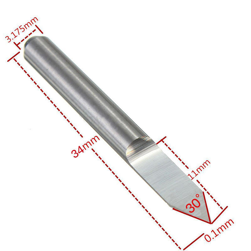
V-shape tool with 30° and diameter of 0.1mm diameter.
Manufacture of PCB test with V-shape tool with 30° and 0.1mm diameter.
We observed that the 0.20mm track and 0.20mm groove were built satisfactorily, so with the selected tool we can build tracks up to 0.20mm thick.
Extra credit: send a PCB out to a board house (I didn’t do this activity)
Individual assignment:
Make an in-circuit programmer that includes a microcontroller optionally customiza it mill and stuff the PCB test it to verify that it works
This week my research focused on the pcb manufacture, mainly in the use of FlatCam software and the manufacturing bits, and also, in characterizing the monofab of the laboratory to know its limitations.
I designed my own pcb for the FabISP with the considerations noted in my test circuit.
To generate the manufacturing commands for the PCBs I used the FlatCam software, I consider it to be easy-to-use software, the only difficulty was understanding the Z-cut calculation for the bit used, which was the tool V-shape with 30° and 0.1 mm, after obtaining the .nc files I uploaded them to the monofab and started the manufacture of the PCBs.
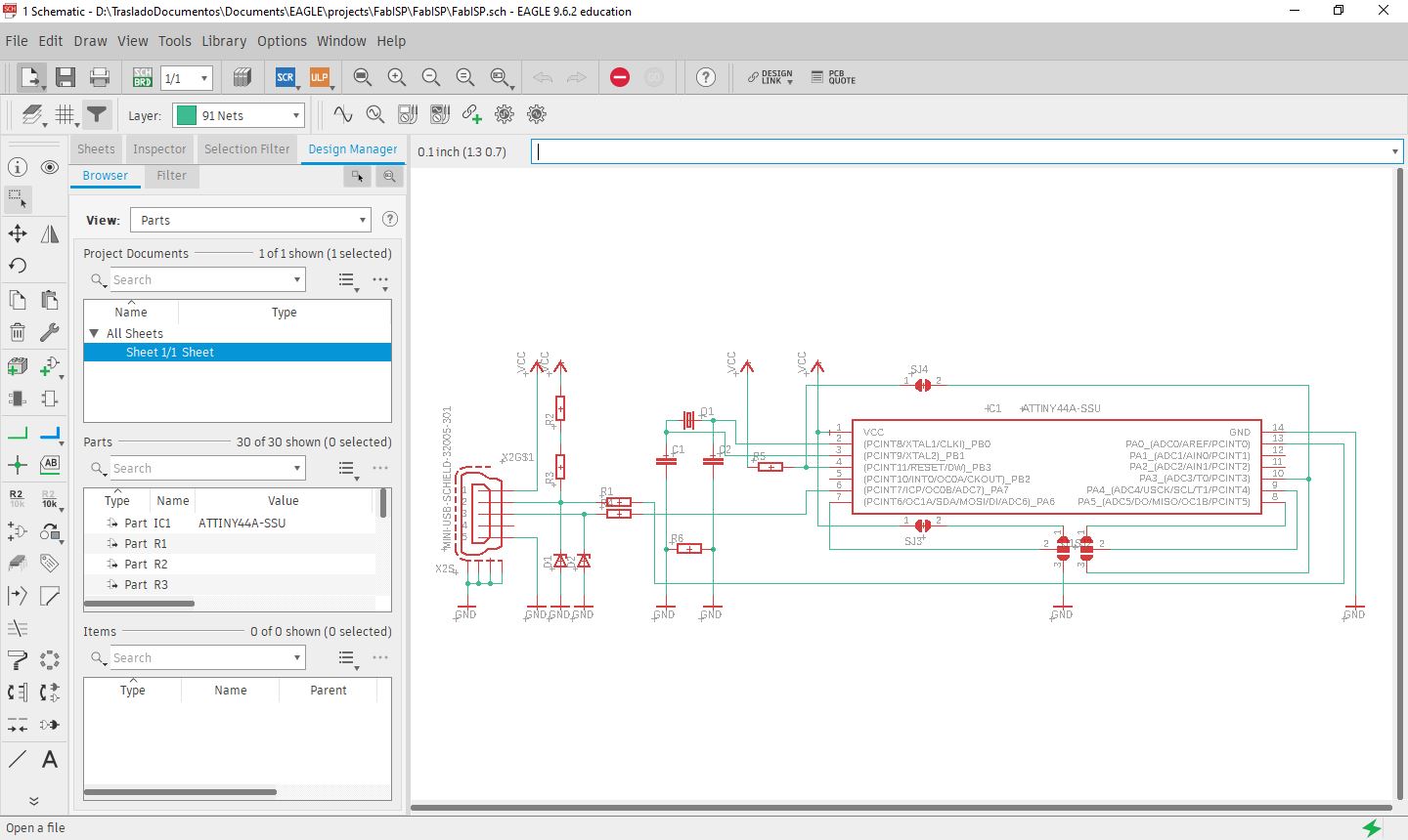
Circuit schematic drawing in eagle.
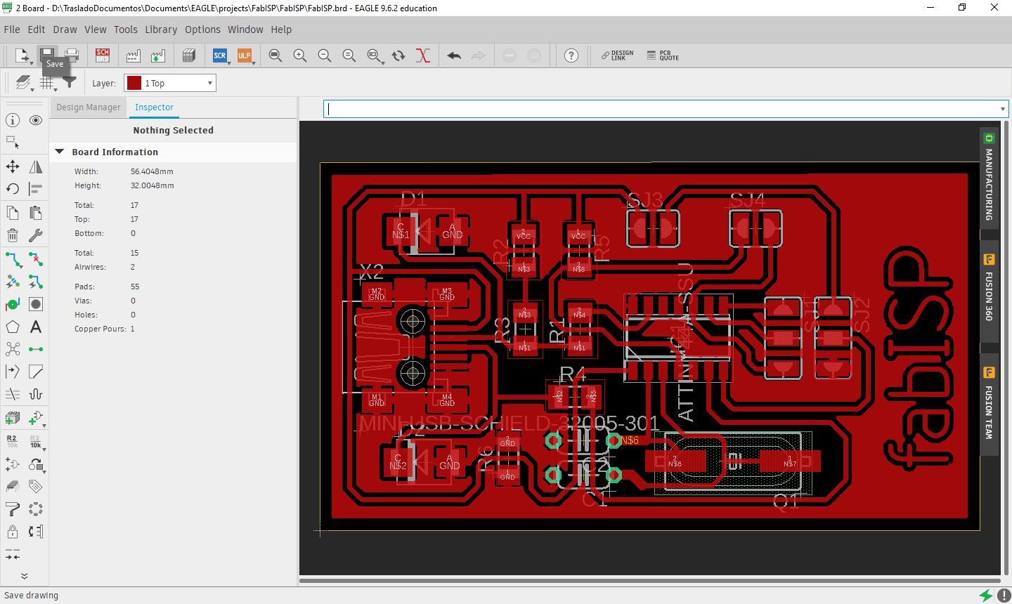
Design of my own PCB.
Getting .gbr files from Eagle to FlatCAM and .nc files for monoFAB
PCB Fabrication in monoFAB CNC - FabIPS Programmer
Perimeter cut and finished PCB
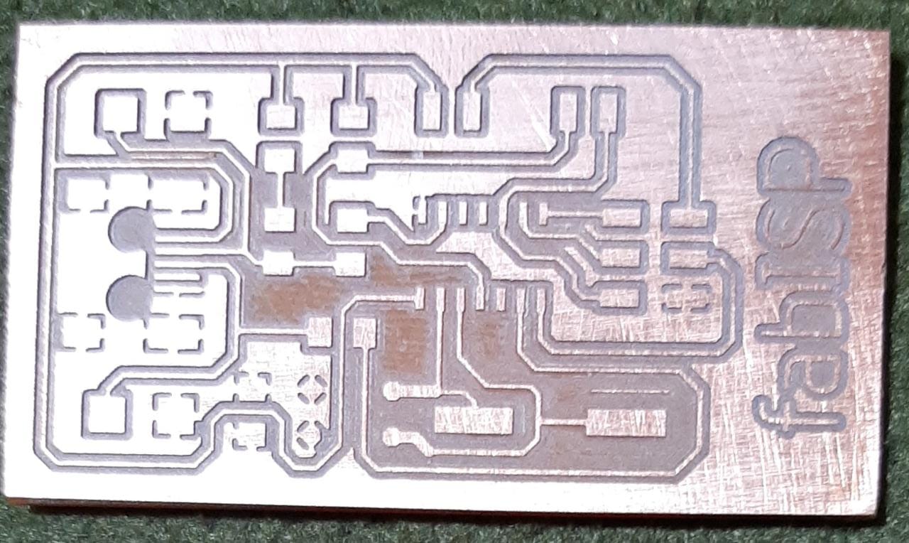
Completion of the manufacture of the fabISP PCB.
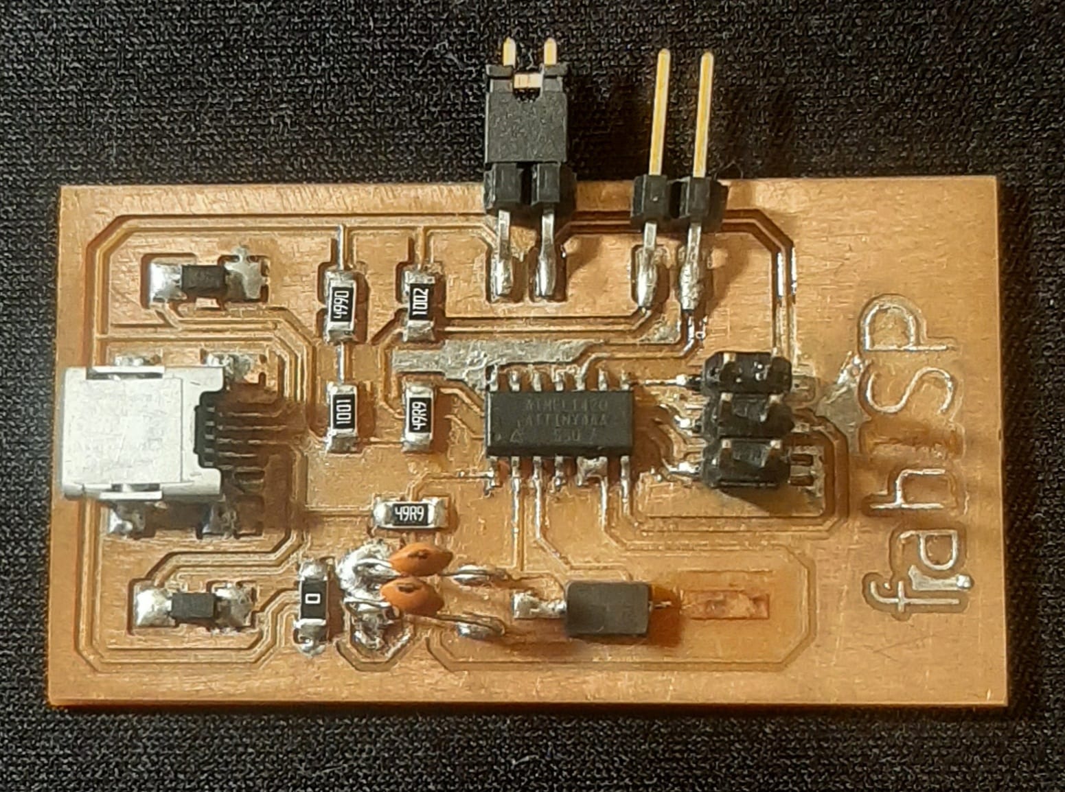
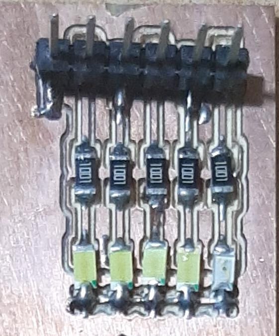
Components soldered on the fabISP PCB.
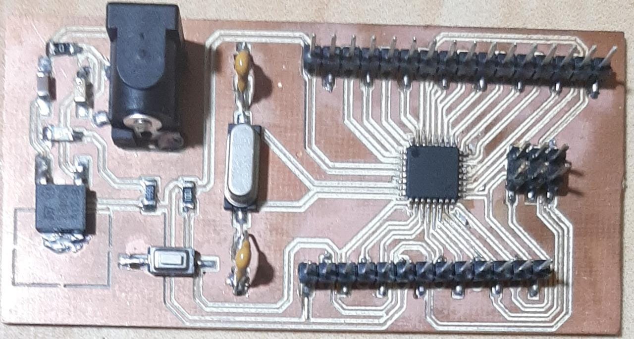
Next, I designed a test board with ATMEGA328P and, I designed a LEDs board both these were used to check functionality my fabISP programmer.
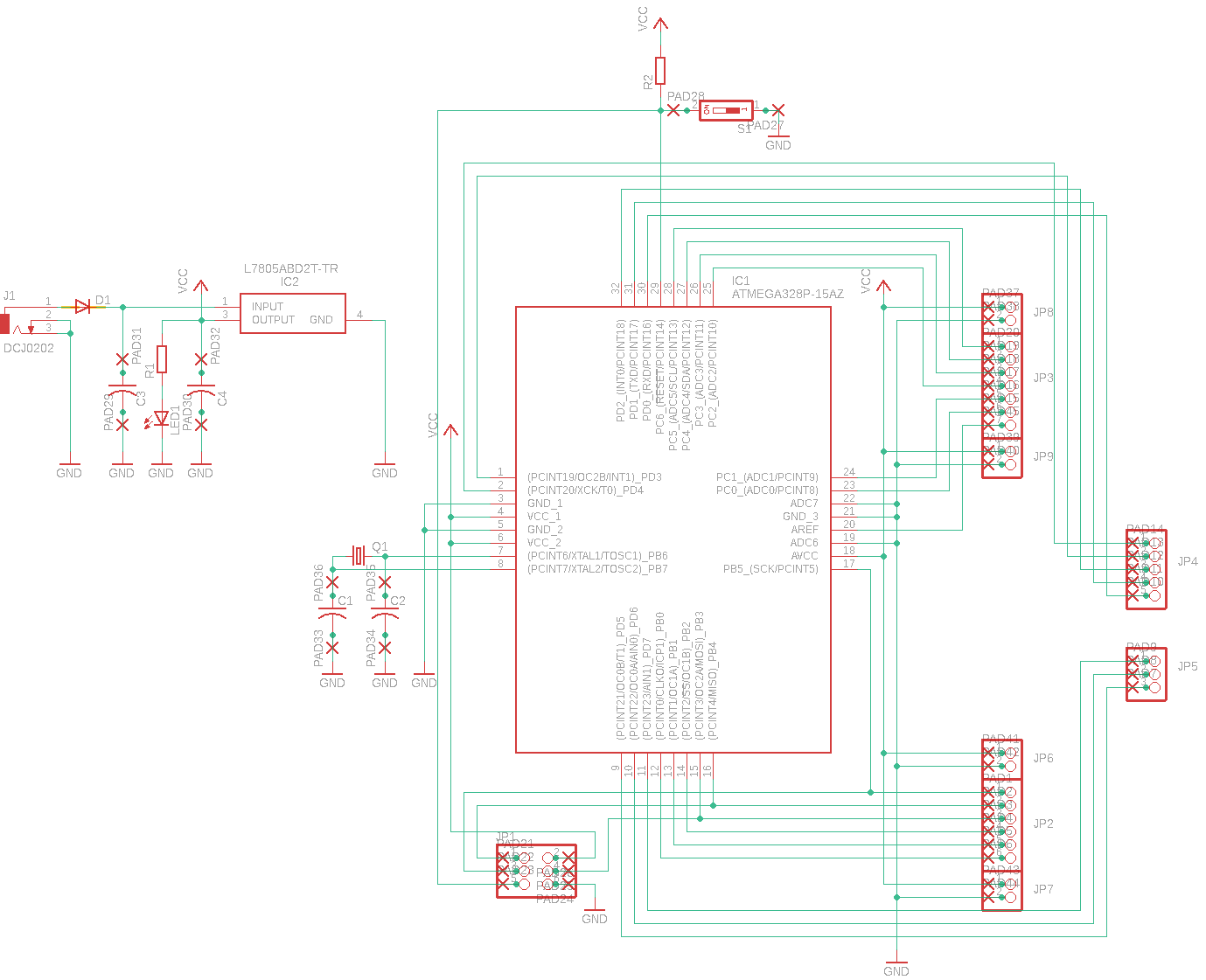
Schematic circuit with ATmega328p microcontroller.

Final design of the connection tracks of the components.
PCB with the components soldered.
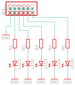
Schematic circuit for five leds.
PCB designed for five leds.
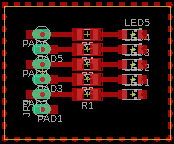
PCB for five leds with the components soldered.
FABISP programmer functionality test
PROBLEMS
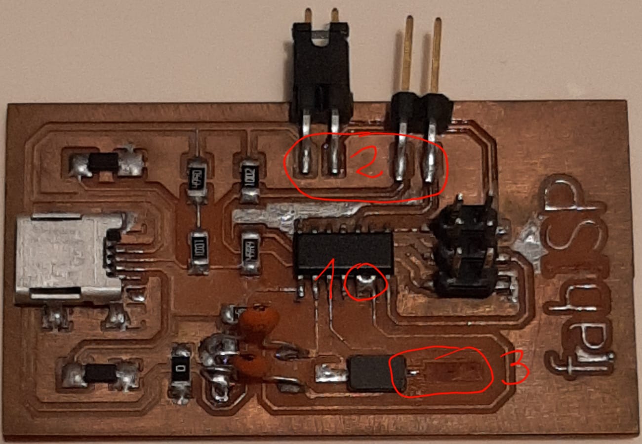
Solution of problems.
- I forgot a connection on the PCB, connect terminals 5 and 6 of the ATTINNY44A, I solved it by making a jumper with the solder.
- The terminal encapsulation was wrong, so I had to change components.
- When I was soldering the components, the copper layer of the pad was lifted, happily I was able to solder the component on the same track.