7. Electronics design
Group project:
Use the test equipment in your lab to observe the operation of a microcontroller circuit board
Output whit LED that shows activation status od button.
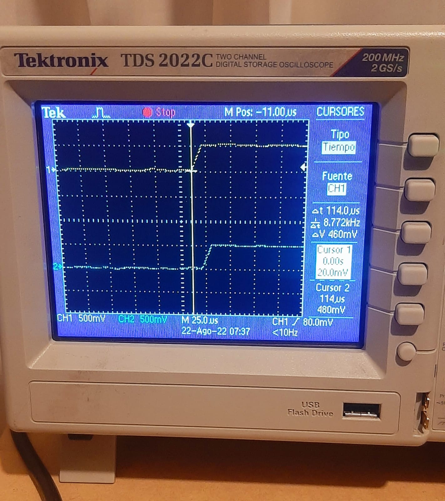
Here, we show the start of button activation.
Here, we show the start of pulse on output. The output pulse has 10us delay.
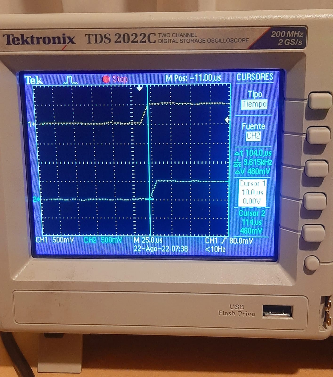
We show the PWM signal generated by the microcontroller.
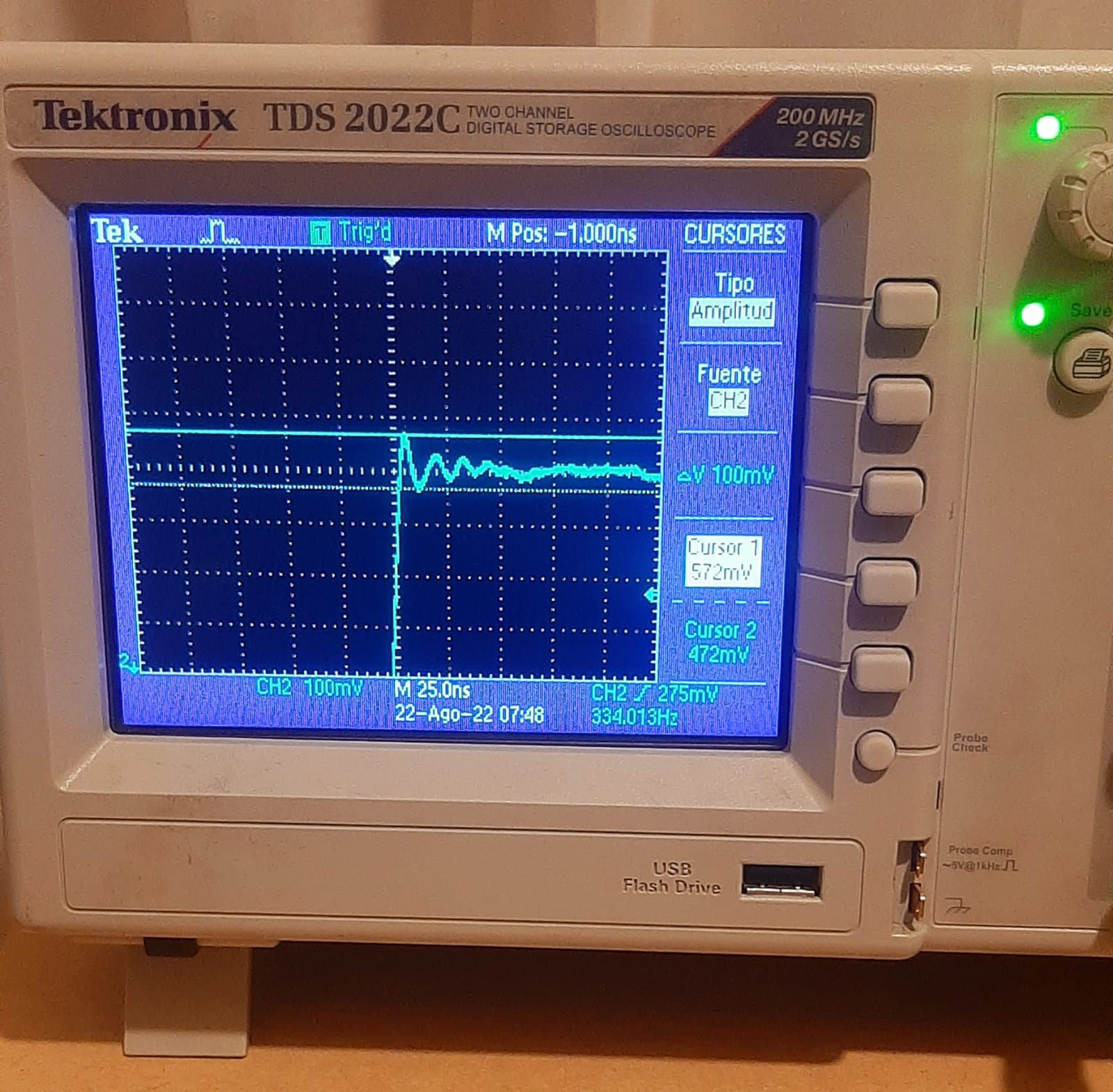
Here, we show the transitory signal of the PWM pulse, we see peak-to-peak values of 100mV.
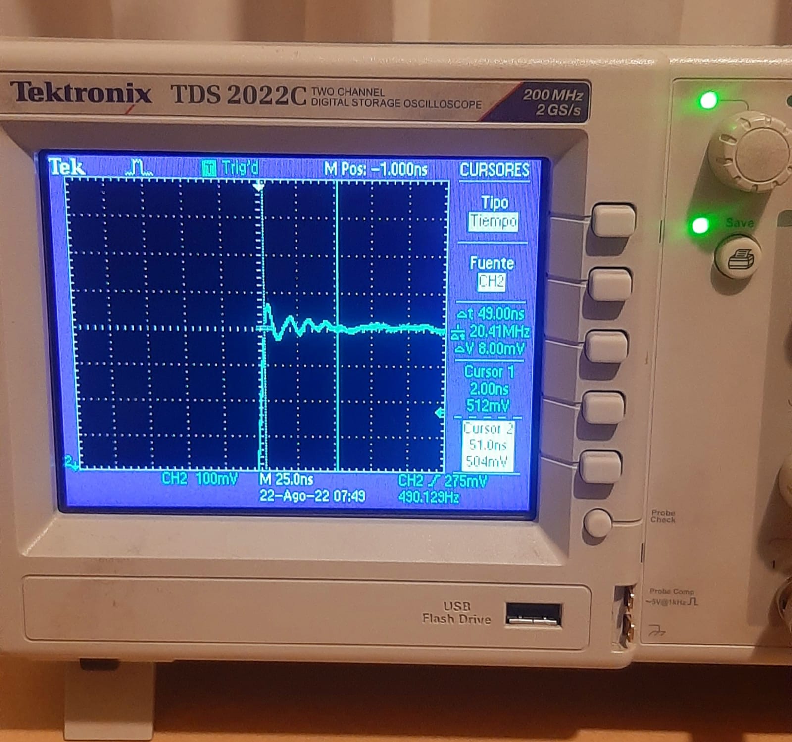
Now, we see the time wide of the transitory signal, it is 49ns.
Individual project:
Redraw an echo hello-world board, add (at least) a button and LED (with current-limiting resistor) check the design rules, make it, and test that it can communicate.
First, I designed a general purpose circuit board with the ATmega328p microcontroller, the design was done in Eagle.
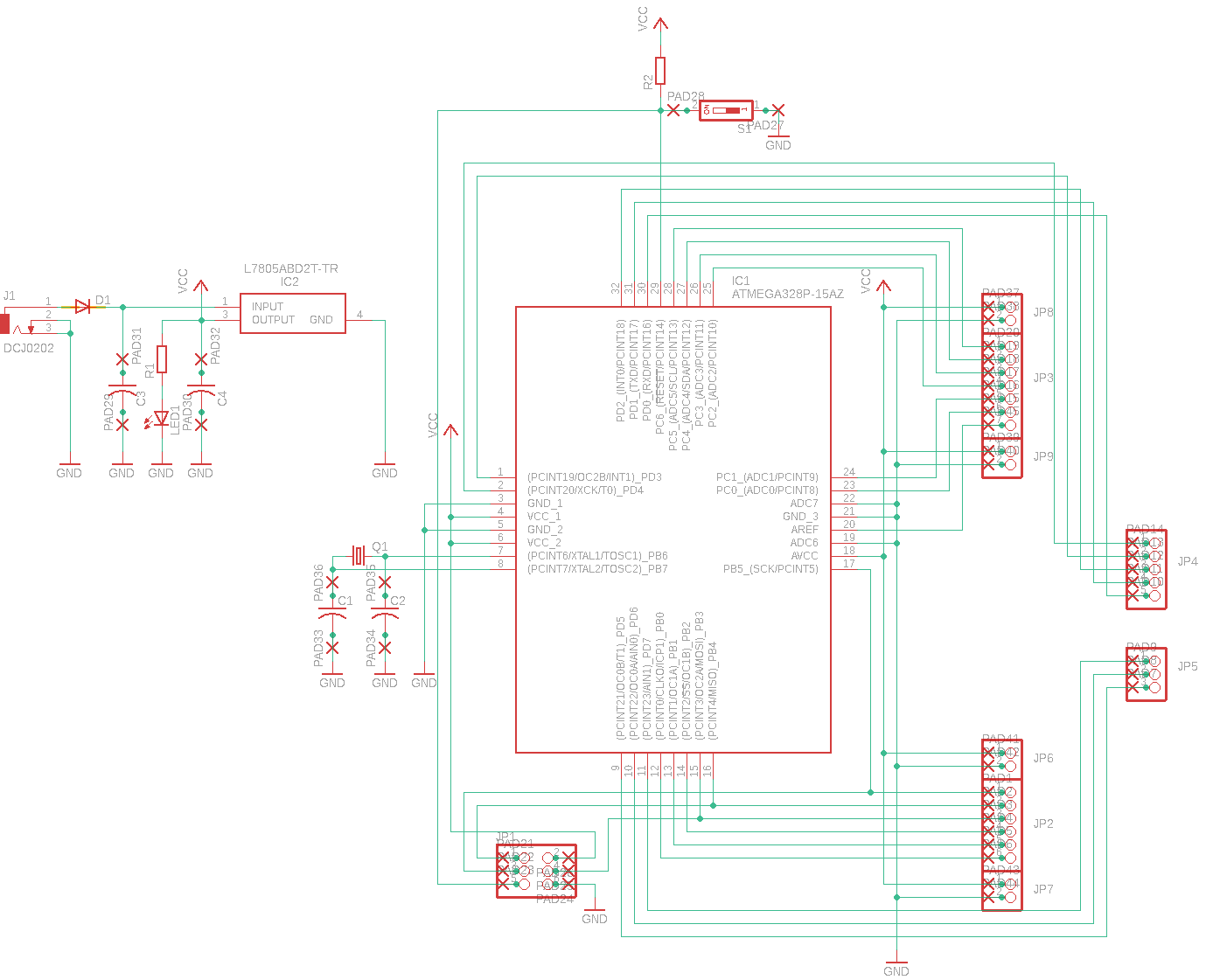
Schematic circuit with ATmega328p microcontroller.
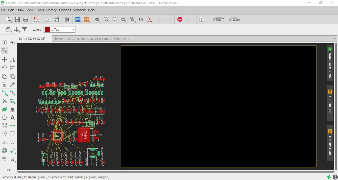
We passed to schematic mode to board mode.
We organize the location of the some components.
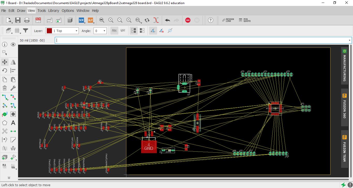
We finished locating all the components.
We start by connecting the microcontroller with some components.
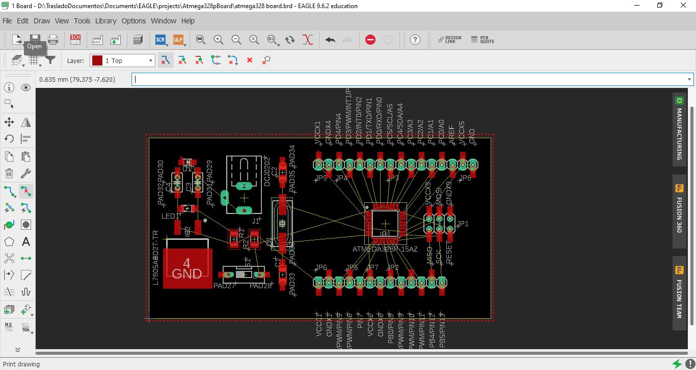
We complete the connection of source and oscillator for the microcontroller.
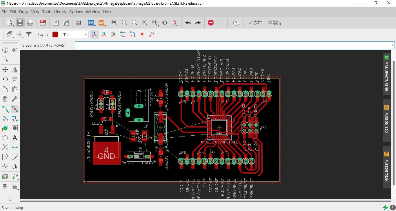
Final design of the connection tracks of the components.
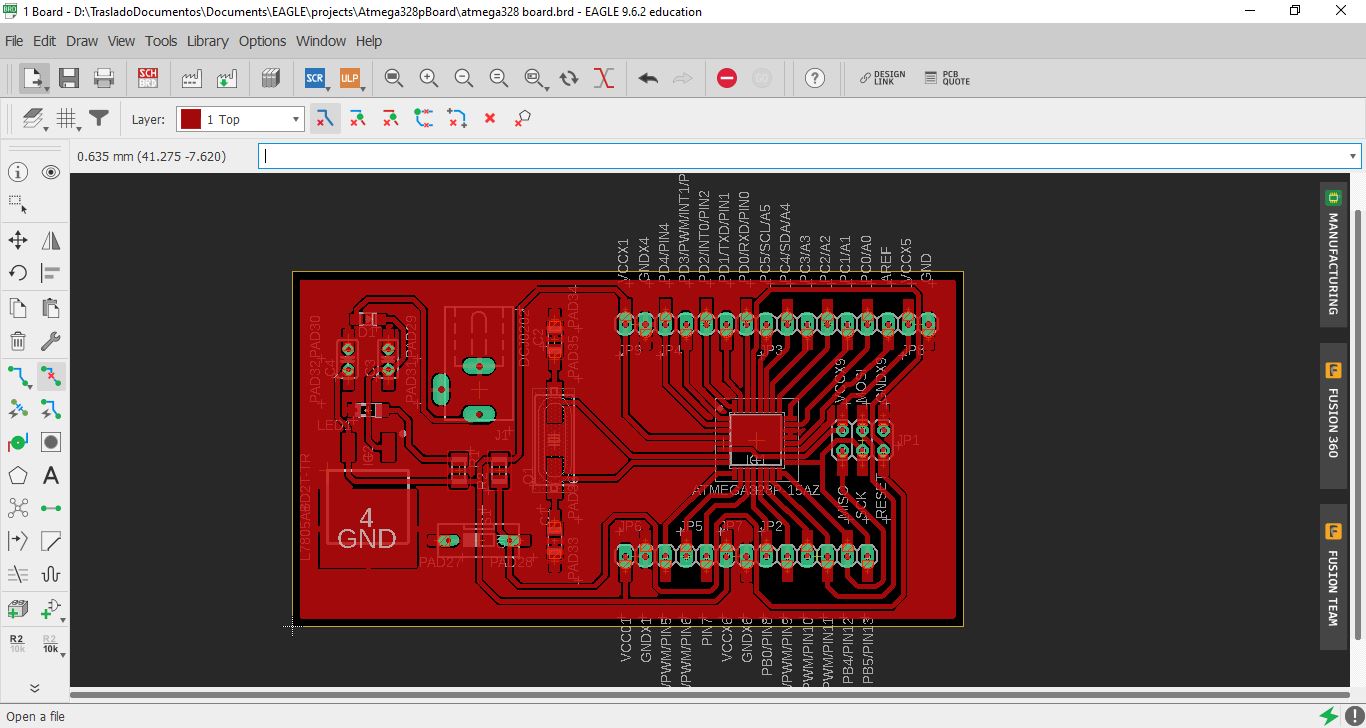
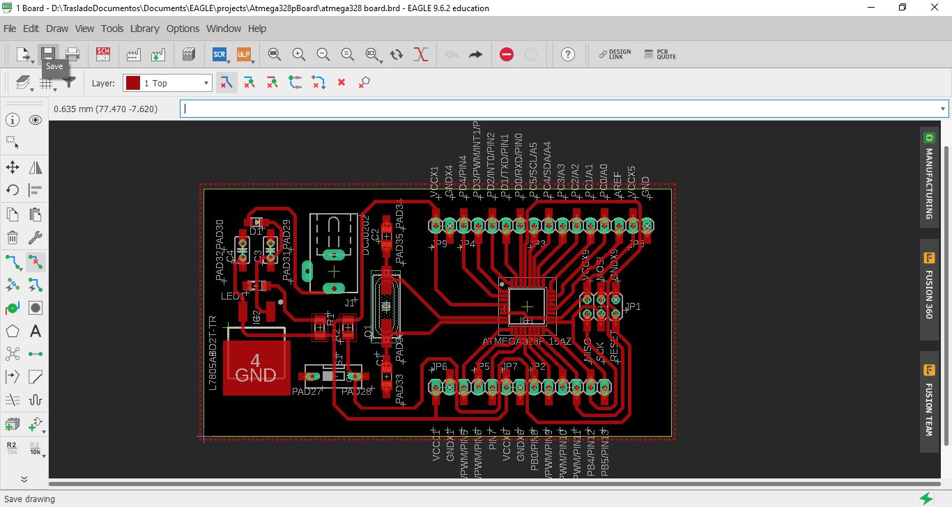
Final PCB layout.
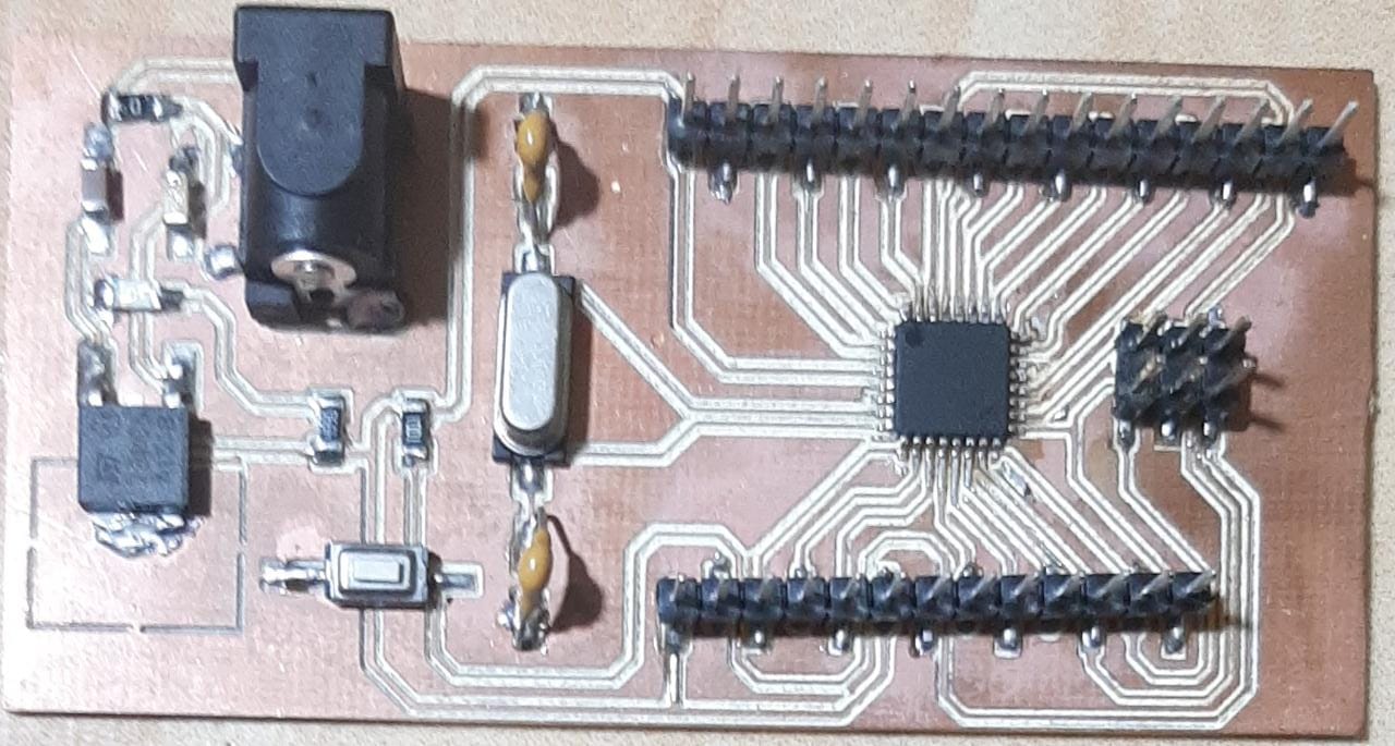
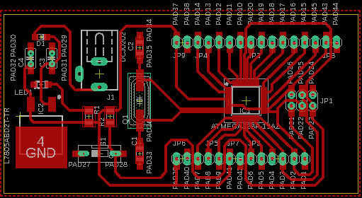
PCB with the components soldered.
Next, I designed PCBs with 4 buttons.
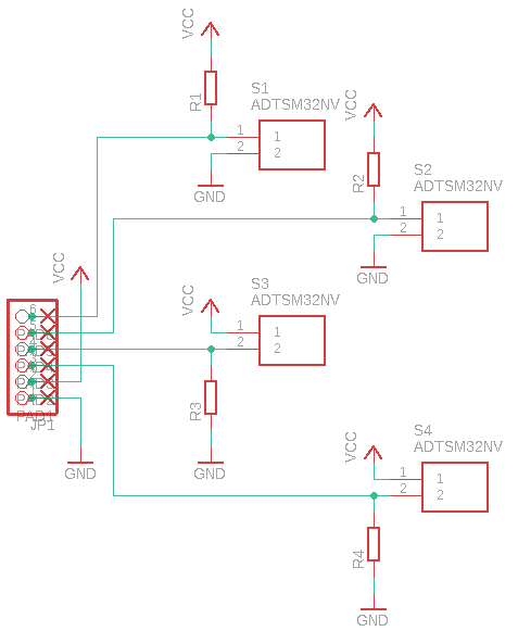
Schematic circuit for four button.
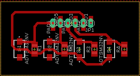
PCB designed for four button.
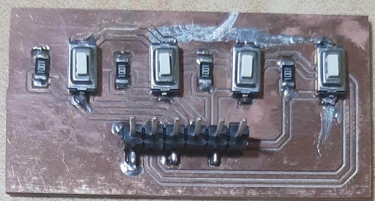
PCB to four button with the components soldered.
Finally, we designed PCB with 5 leds and 5 resistors
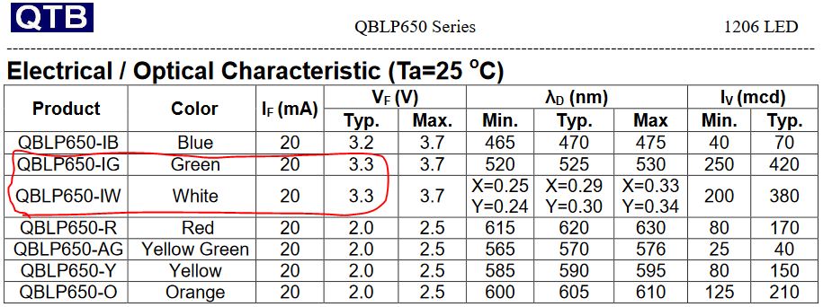
The table shows the voltage drop of the green and white-yellow LEDs, this is 3.3v.
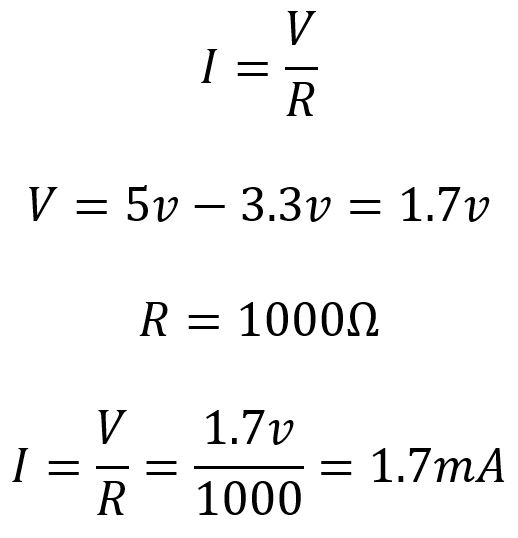
Ohm’s law for current calculation, we also consider 1kΩ value resistor. We get a current of 1.7mA
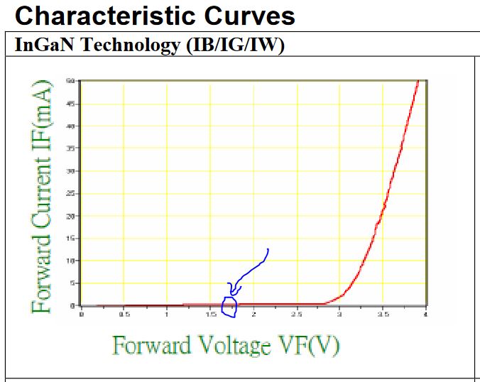
We check that the calculated current is within the forward bias curve of the diode.
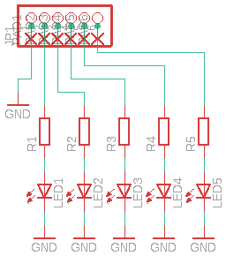
Schematic circuit for five leds.
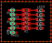
PCB designed for five leds.
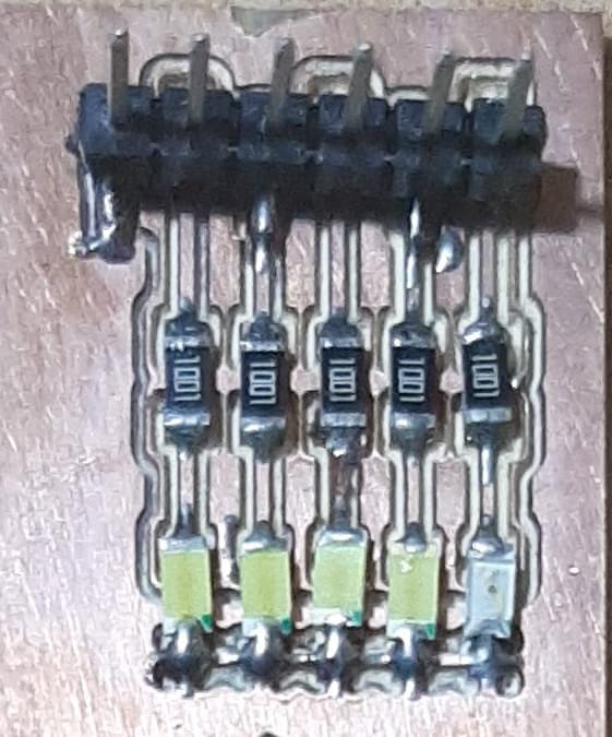
PCB for five leds with the components soldered.
Code Example
bool PIzq = false, PDer = false, PSS = false;
int leds[] = {1, 2, 3, 4};
int pulsadores[] = {5, 6, 7};
int retardo = 250, tiempoActual, tiempoAnterior=0, j=-1;
void setup() {
  // put your setup code here, to run once:
  for (int i=0;i<=3;i++){
    pinMode(leds[i],OUTPUT);
    pinMode(pulsadores[i],INPUT);
    digitalWrite(leds[i],LOW);
  }
  pinMode(0,OUTPUT);
  digitalWrite(0,LOW);
}

void loop() {
  // put your main code here, to run repeatedly:
  if (!digitalRead(5)){
    if (PDer){
      for (int i=0;i<=3;i++){
        digitalWrite(leds[i],LOW);
      }
      j=-1;
    }
    PIzq = true;
    PDer = false;
  }
  if (!digitalRead(6)){
    if (PIzq){
      for (int i=0;i<=3;i++){
        digitalWrite(leds[i],LOW);
      }
      j=-1;
    }
    PIzq = false;
    PDer = true;
  }
  if (digitalRead(7)){
    delay(50);
    PSS = !PSS;
    digitalWrite(0,PSS);
  }
  if (PSS){
    if (PIzq && !PDer){
      tiempoActual = millis();
      if(tiempoActual-tiempoAnterior >= retardo){
        tiempoAnterior = tiempoActual;
        j++;
        if (j==4){
          j=-1;
          for (int i=0;i<=3;i++){
            digitalWrite(leds[i],LOW);
          }
        } else {
          digitalWrite(leds[j],HIGH);
        }
      }
    }
    if (!PIzq && PDer){
      tiempoActual = millis();
      if(tiempoActual-tiempoAnterior >= retardo){
        tiempoAnterior = tiempoActual;
        j++;
        if (j==4){
          j=-1;
          for (int i=0;i<=3;i++){
            digitalWrite(leds[i],LOW);
          }
        } else {
          digitalWrite(leds[3-j],HIGH);
        }
      }
    }
  } else {
    for (int i=0;i<=3;i++){
      digitalWrite(leds[i],LOW);
    }
    PIzq = false;
    PDer = false;
    j=-1;
  }
}
Video of the HELLO-WORLD boards with buttons and leds.
Extra credit: simulate its operation.
Circuit simulation was done in Proteus.
DRC Design Rule Check and ERC Electrical Rule Check in EAGLE
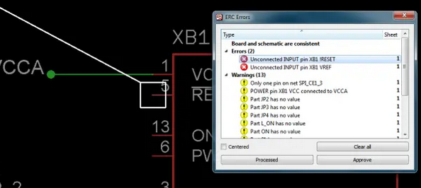
When we have our schematic diagram finished, before proceeding to trace the tracks or routing, it is recommended to check the schematic errors with the ERC (Electrical Rule Check).
PCB for five leds with the components soldered.
The yellow button at the bottom of the tools menu is pressed.
PCB for five leds with the components soldered.
Automatically finds potential errors in the design and groups them as errors or warnings

PCB for five leds with the components soldered.
Selecting with double click on the error or warning places us directly in it.
PCB for five leds with the components soldered.
It is recommended to review them one by one, since we can find errors that are simple to correct and that can save us money and time in a later rework. Not all errors or warnings are serious, in the example of the image, the product was already manufactured and those errors were considered irrelevant.
Common design errors include missing values for elements such as resistors or capacitors, crossing two signals without a physical connection, etc.
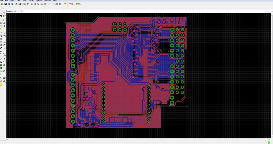
For the boardfile, the errors are more important and critical, for this, once the design has been completed, we proceed to activate only the layers that we want to analyze (This way we do not add noise to the program and we only see the layers that could physically cause problems ). In this case we recommend selecting only:
 Top
 Bottom
 pad
 roads
 Dimension
PCB for five leds with the components soldered.
Subsequently, the DRC (Design Rule Check) button is selected at the bottom of the tools menu

PCB for five leds with the components soldered.
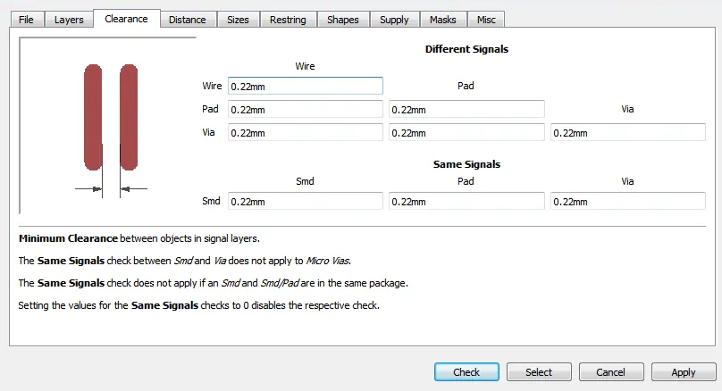
Next, the window corresponding to the PCB DRCs appears on the screen.
PCB for five leds with the components soldered.
It is recommended to review all the tabs in detail. We do not recommend changing any of these parameters unless you really understand what you are doing.
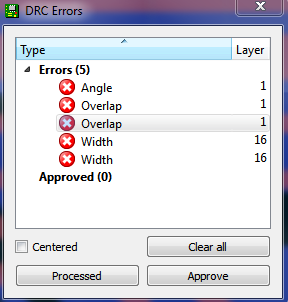
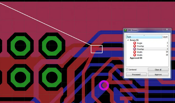
To load the errors, just click on Check. Subsequently, a list of errors that the program detected appears.
PCB for five leds with the components soldered.
It is recommended to fix a couple of bugs and reload the DRC because moving a net or track can generate more errors for other reasons.
Once the errors have been corrected, the gerber files can be generated for manufacturing. By reviewing the DRC it is possible to greatly reduce the errors that arise when creating the boardfile.
Double-click each of the errors to be able to select and center them on the screen.
PCB for five leds with the components soldered.
Useful links
- QBLP650 Series LEDs datasheet
- A Basic Introduction for Designing a Printed Circuit Board (PCB) with EAGLE eCAD/CAM Software