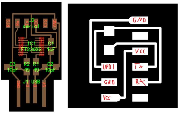
This week's assignment was to redesign the USB to FTDI programmer and add an UPDI to it. For reference I used the hello.USB-UPDI.FT230X from fab academy and UPDI adapter for that from Adrián Torres's Adrianino project. For the second and third versions of the board I also used Antti Mäntyniemi's design as a reference.
Fab academy FTDI board on the left and Adrián's UPDI adapter on the right
Before I started designing, I downloaded a new version of KiCad and the Fab Lab library for it. I later noticed that I had completely skipped or made a mistake in the custom 3D shapes setup. To fix that I just followed the library installation guide.
In the KiCad I made a new project called programmer. After I had made a mistake that broke my PCB file I also decided to use Git for version control.
KiCad relies heavily on the hotkeys so I googled a cheat sheet. Here are some of the useful ones in the schematic editor: A Add components W Add wire V Change value L Add Label R Rotate M Move G Move but keep the wires connected. Works only with one component and wires can get messy. TAB Same as G but for selected area. First version of the schematic
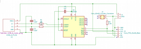
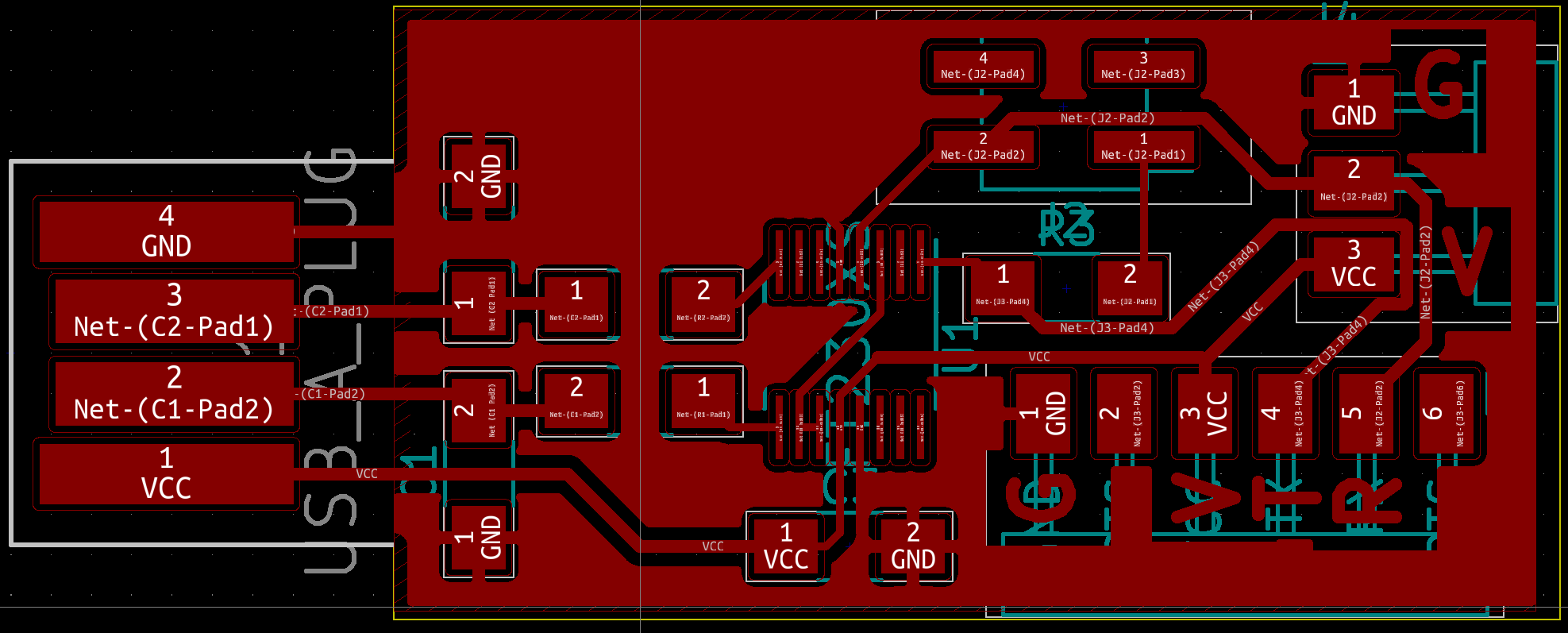
I added the components from the Fab library to schematic. The only thing that wasn't in the Fab library was the 2x2 connector for the jumper. The jumper was added so you could disconnect the resistor that connects the FTDI signals, RX and TX, for the UPDI signal. The connector itself was just a 2x2 connector with counterclockwise pin numbering. It was from the Connector_Generic library. Somehow I had completely forgotten the VCC and GND symbols and had wired the voltages directly to the USB connector. I wired everything, did the annotation and the electrical rules check. I had forgotten to place the No connection flags to the unused pins. I flagged the unused pins and the check was clear. Then I could generate the netlist move on to the PCB design.
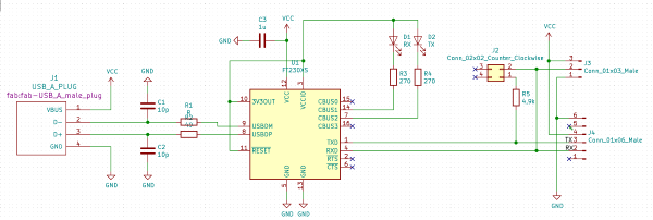
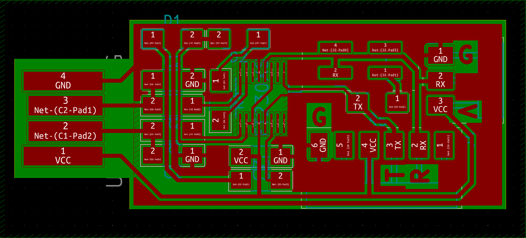
I made the schematic again with the VCC and GND symbols. I also added TX and RX LEDs. This turned out to be stupid idea and I will talk about it more in the PCB part. I also changed the FTDI connector to normal 1x6 header so I could change the order of the pins. This was done after discussing about it in our course.
LED version of the schematic
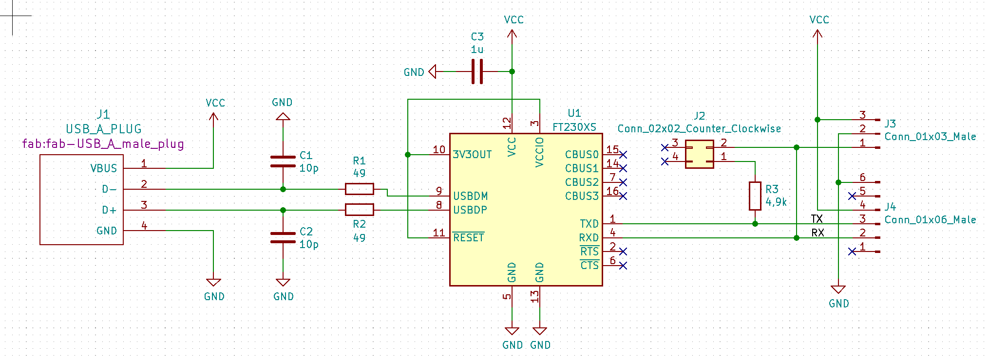
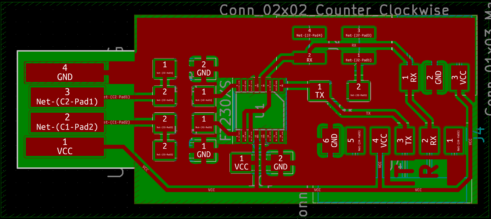
I made a new version where I removed the LEDs and changed the UPDI connector to same pinout as Antti's design. I opened the assign PCB footprints to schematic symbols menu. There I changed FT230XS chips footprint to regular SSOP footprint because I had a lot of trouble trying to mill the narrower pads that were used in the fab lab library. I also added a footprint to the jumper connector. I used a SMD vertical pin header.
Final version of the schematic
I learned that in the current version (5.1.9) of KiCad you don't need to make a netlist anymore, you can just click the Run Pcbnew to layout printed circuit board button to open the layout editor and it imports the circuit from the schematic.
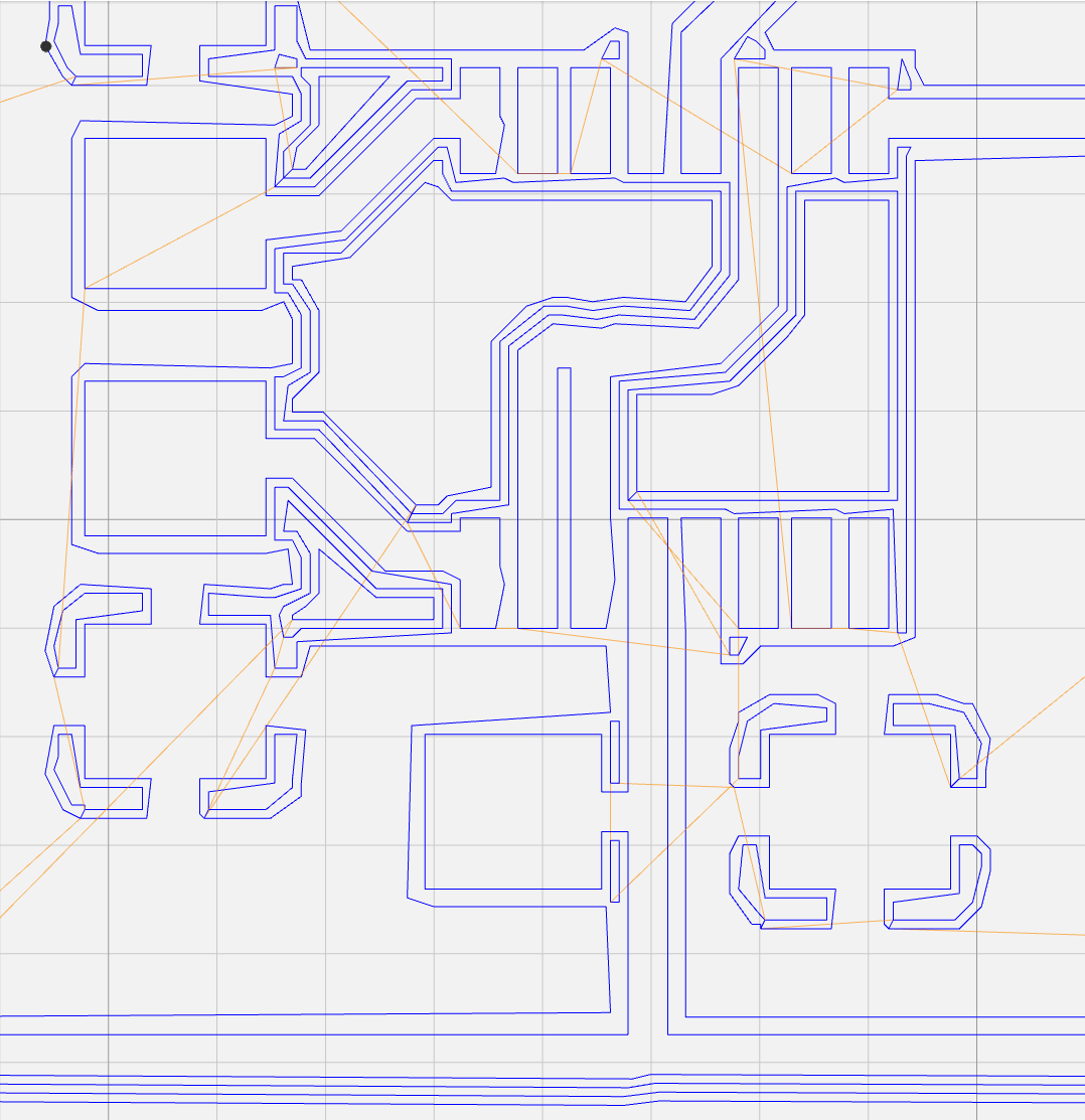
Some useful hotkeys: R Rotate M Move X Route tracks W Increase track width Shift + W Decrease track width N Decrease grid size Shift + N Increase grid size B Update/fill filled areas Control + B Unfill filled areas One of the early version of the layout
First I tried to decide the parts position and to check could I get everything wired without any jumper wires. I could so I packed the components closer and added a ground fill area. I also added some labels to the copper layer. I didn't like how the text takes a whole rectangle of space. I found this post on reddit where they imported text as art to other layer and then changed that layer in text editor to be on copper layer. This worked but I managed to break the connection between the project file and the PCB file during that process. The whole process is a bit cumbersome and hack so I didn't do it again. There was also a lot of room on the upper left part of the board that I couldn't really get any smaller so I decided to try to add TX and RX LEDs. I made a completely new version of the programmer since my files were already broken.
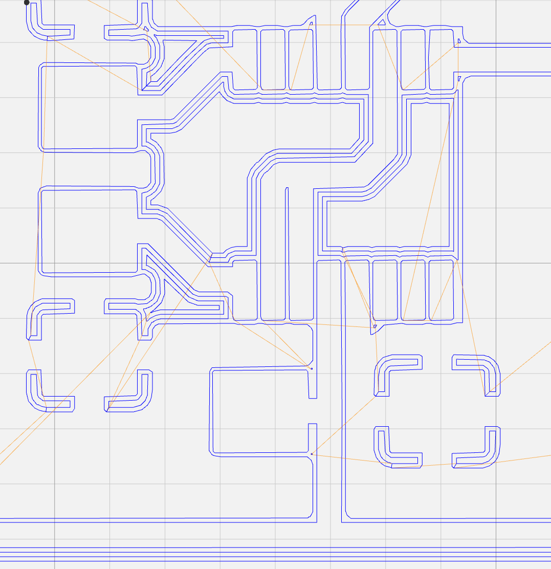
LED version of the layout
In this version I had also made a filled area in the Eco1.User layer. I changed the width of this filled area to 0 mm because I thought this would give me area equal to the size of the edge cut. This setting gives the size of the inner area of the edge cut and 0,005 mm gives the area equal to the outer edge of the edge cut line, as Antti pointed out. For this application I think both would have worked and since I don't even know how the MODS handles the outline and its offsets it is pretty useless to try to make a precise board. In the end this board didn't work out because of the small pads and I think the three tracks under the 1206 components were stupid too.
Final version of the layout
For the final version I changed the UPDI pinout to match Antti's design, changed the FT230XS pads and tracks that connected it to be wider. The wider tracks made milling the board a lot easier. Gradually my design had begun to look more and more like Antti's design. The general placement of the parts I just copied from Antti because I couldn't figure out a better layout myself.
The only real differences in my design are the wider tracks for the FT230XS chip and the labeling of the TX and RX pins.
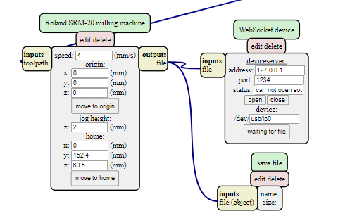
WebSocket device module needs to be replaced with file save module. The origin in the Roland SRM-20 milling machine module needs to be changed to 0, 0, 0 mm.
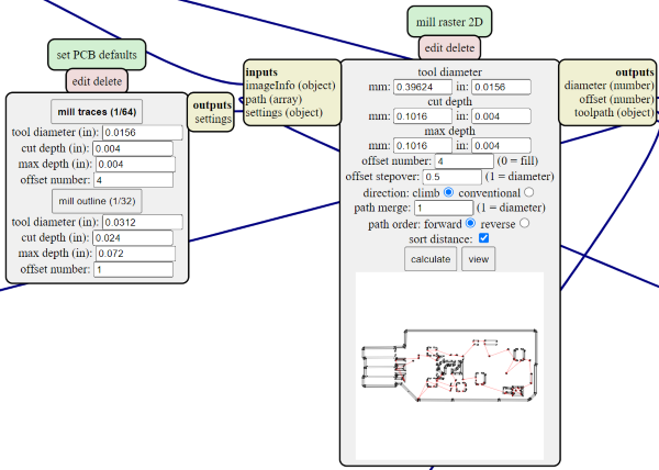
I went to the MODS website. I opened the menu with the right click and selected the PCB SVG program. The path to that is programs, open server program, Roland, mill, SRM-20, PCB SVG. The mill we were going to use was Roland SRM-20. When it was open, I deleted the WebSocket device module since I wasn't going to send the job directly to the milling machine. I added a new module to save the file module, open server module, file, save. I didn't connect it yet to the Roland SRM-20 milling machine module because I didn't want to save all the iterations that I had to do. Then I changed the origin in the Roland SRM-20 milling machine module to 0 mm in every axis. Then I opened the copper layer SVG with the read SVG module. I inverted it in the convert SVG image module.
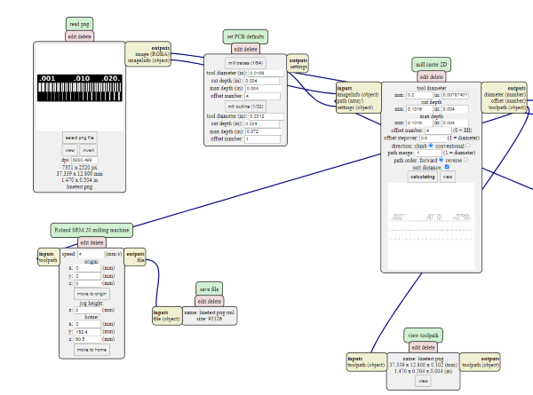
I used set PCB defaults module to define that I want to cut traces. The only setting that matters to my knowledge is the option between the mill traces and mill outline options. It sets at least the offset number to correct value, I don't know if there are any invisible values affected. In Fab Lab Oulu 0.2-0.5 mm millimeter V-bit is used to cut the traces. You want to have as large tool diameter in mill raster 2D module as possible. You can see the traces I wanted in the SVG image below and the first iteration below that. I had to use 0.20 mm tool diameter to get the cuts I wanted. Now I could connect the save file module and save the RML.
Traces in SVG. Actual SVG I used was black and white, this is red just for documentation.Milling modules in MODS
For cutting out the board I opened the filled outline SVG, inverted it, used the mill outline setting, 1 mm tool diameter, 0.6 mm cut depth and 1.7 max depth.
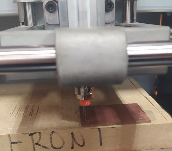
I had a lot of trouble trying to mill the PCB but after a few changes in design and a new day I got a good result from the first blank.
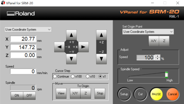
Roland VPanel is used to control the mill
Antti had used the retractable blade to cut the blanks smaller so you wouldn't need to use as much tape and you would also have a better chance to set it straight to the milling machine. After my classmate Toni Kyllönen had made a clean cut with guillotine, I also started to use it to cut the blanks. I used double-sided tape to glue the blank to the mills sacrifice plate. Before that I had looked that the blank looked straight. After gluing the blank I inserted the trace milling bit to the chuck. The bits are made out of "premium carbide" so they are hard but brittle and need to be handled carefully. While the Z-axis was still up I used the Continue step mode to move the X- and Y-axis near the bottom left of my blank. Then I changed to the x100 mode to move the milling bit closer to the blank so I could see the milling bits position better.
I then adjusted my X- and Y-axis to the origin and set it with Set Origin PointX/Y button.
Then I moved the Z-axis close to the blank. After that I held the milling bit with one hand and loosened the chuck with other hand. Then I gently lowered the bit so it touched the surface of the blank. I set the Z-axis origin and after that I raised it 0.2 mm. The cut depth in MODS was set to 0.1016 mm so this was too high but it is better to be too high than too low. Then with the Cut button I deleted the old files and added my own. With the Output button the cutting started.
As I said before the Z-origin was too high for the cutting depth, so I canceled the cut and lowered the Z-axis origin by 0.2 mm. I used the View button to move the milling bit so it wasn't over anything and then used the To Origin Z button to get the Z-axis to a know position where I could lower it. This was maybe too much or maybe I didn't stick the blank to the mill firmly enough but the blank separated from the mill and I had to cancel the cut. After this I started to lower the Z-axis only 0.02-0.04 mm per time.
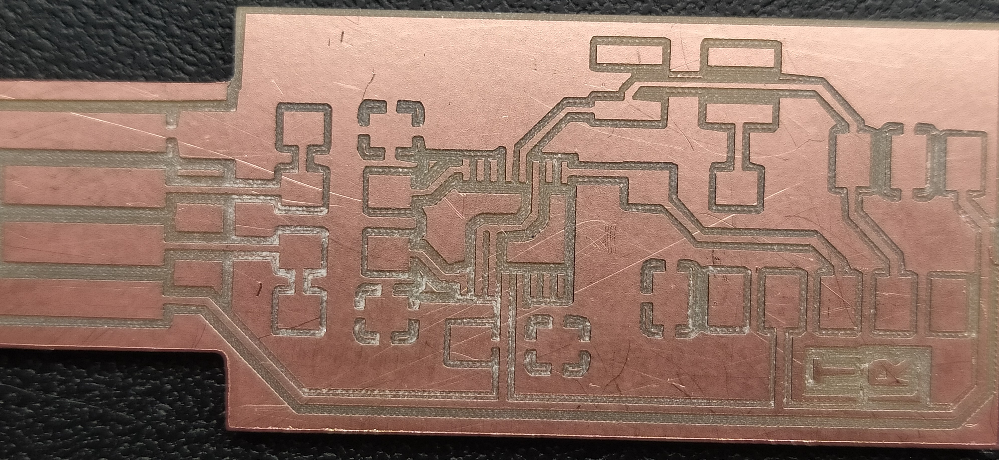
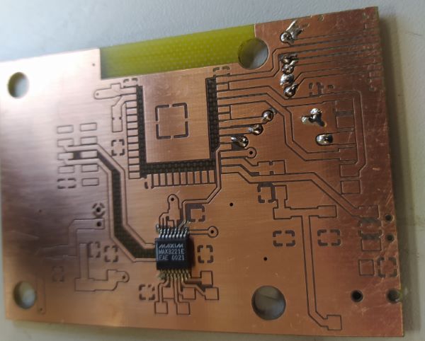
PCB that I knew I could fix with knife. You can see that even here the trace under FT230XS is almost broken.
The PCB I first tried to mill was the version with TX and RX LEDs and with narrow FT230XS pads. These pads and all the narrow traces under the 1206 components felt like too hard to mill. So I tried to use the PCB and RML files that Antti had made. Even with that design I couldn't get a good result, either the mill wouldn't mill around all the traces or the mill would cut the smaller traces. I think it was my fifth try when I got a result that I knew I could at least fix with a knife.
PCB that I used to assemble the programmer
I went home and redesigned the PCB with wider pads and traces and I also removed the leds. With this new design I got a my best result yet on the first blank. I couldn't say in the first try, because I still slowly lowered the Z-axis between each pass to get all the traces milled. I wasn't completely happy with this result either. I can see that the mill left quite a lot of small areas milled, this is very noticeable on the long VCC trace at the bottom of the board. At this point I was too eager to get to finally assemble the board so I just tested that there weren't any shorts and scraped the worst parts out.
Weird stepover behavior
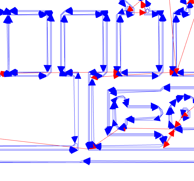
The results looked like the stepover were a bit too large. In MODS you can adjust the offset stepover but that doesn't seem to affect the regular stepover. You can see this in the image below where I used 0.2 mm tool and 0.1 stepover, which is 10 % of the tool size. You can see that the stepover on the left side of the vertical trace seems to be much larger than the stepover in areas where the MODS is doing its offset calculations. These settings were just for demonstration.
After discussing about this in the feedback session, I wanted to test if the higher DPI would help. I generated two NC files in mods, one with 500 dpi which is the default and one with 2000 dpi. I used NCViewer to view these toolpaths. There was a huge difference in the generated toolpaths.
Toolpaths when using 500 dpi which was the defaultToolpaths using 2000 dpi
It is still a bit mystery to me why would you convert an SVG image to lossy PNG image to generate toolpaths but that is what the MODS does. Then the MODS runs some edge detection algorithms to generate the paths again.
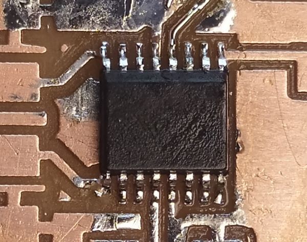
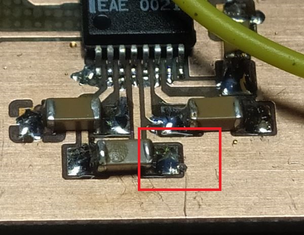
FT230XS soldered to the board
Before I started to solder anything, I tested that there weren't any shorts between the traces with the beeper. Then I sanded the board with sandpaper. The sandpaper was just a piece lying on my table and it didn't have the roughness printed to it but my guess is it was somewhere between P500-P1000. I first soldered the FT230XS chip and had some trouble trying to get it to sit straight on the pads. I managed to bend some pins while doing that. You can see those on the edges on the bottom row on the picture above. You can also see the excessive amount of flux that has dried over the chip. I tested the connections with the beeper and everything seemed fine. Everything else in the soldering process went quite smoothly.
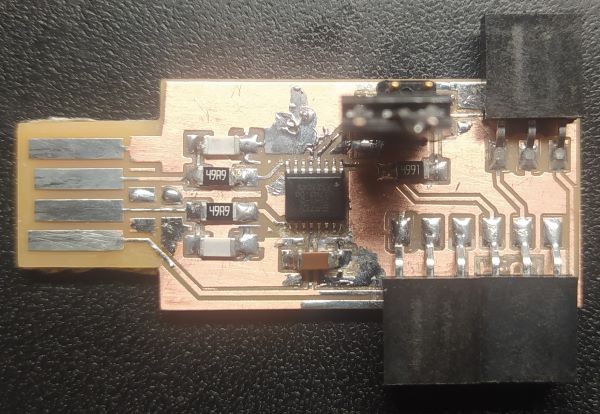
Assembled board
I cut the extra copper left around the USB pads and covered the pads with tin as Antti had instucted. I used the male pin header and different board to hold the female headers straight while soldering them. Juha-Pekka Mäkelä had found me an jumper in Fab Lab but I forgot to take it with me so I made one from the 1x3 female header. I added some masking tape under the board so I would get a good fit in the USB. When I had assembled the board I decided to clean some of the extra copper between traces. While doing this I managed to cut one of the USB data lines. I fixed this with solder, you can see it in the image above. I didn't have any IPA at home, so I cleaned the board with Bräkleen and it seemed to work well.
When I plugged the programmer in to the PC it recognized it as an USB serial port but I couldn't get the programmer to send or receive anything. I first tested it by just shorting the TX and RX pins but I didn't get any response in the PuTTY where I had opened the serial port. I tested the connections between the chip and the pins multiple times with the beeper and they seemed fine. Then I connected the board to my commercial USB-UART device and got it to receive messages but not to send anything. Then I thought that maybe when I was measuring the connection I applied pressure to the pins and that's why the beeper would show connection but there could still be a loose connection when using the programmer. I checked the chips solder joint under macro lens and there seemed to be a bit dry solder joint so I reflowed them and got the board finally working as intended.
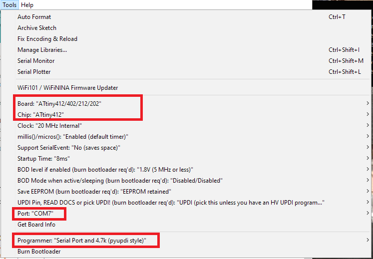
I added the megaTinyCore to the Arduino IDEs additional board manager URLs which can be found under File -> Preferences. I installed the megaTinyCore from Tools->Boards->Boards Manager....
Settings for the UPDI and AT412
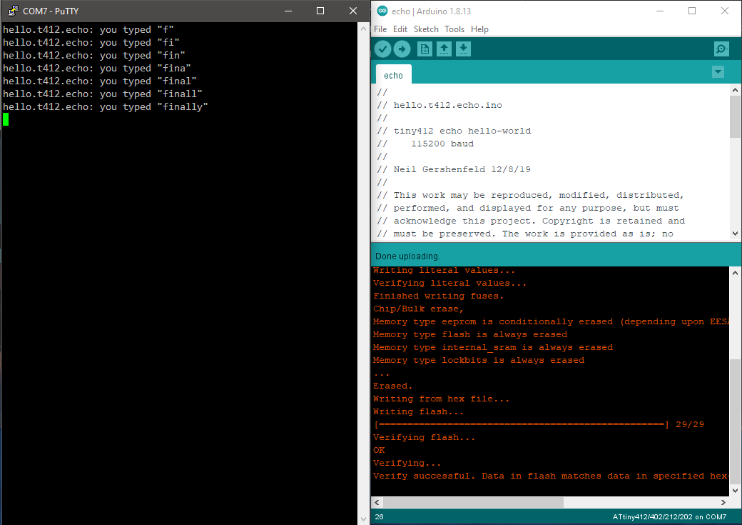
I had made my own version of the hello.t412.echo board so that I had the correct UPDI pin out. I copied the echo.ino to Arduino IDE changed to correct settings that you can see from the image above and uploaded it to my board. Then I unplugged the echo board from the UPDI and changed it to the FTDI side. I opened PuTTY and it worked.
Uploading the code in Arduino IDE and serial communication in PuTTY
I used linetest.png and generated the toolpaths for SRM-20 in Mods. For the milling I would use a two fluted 0.2-0.5mm V-bit.
Mods
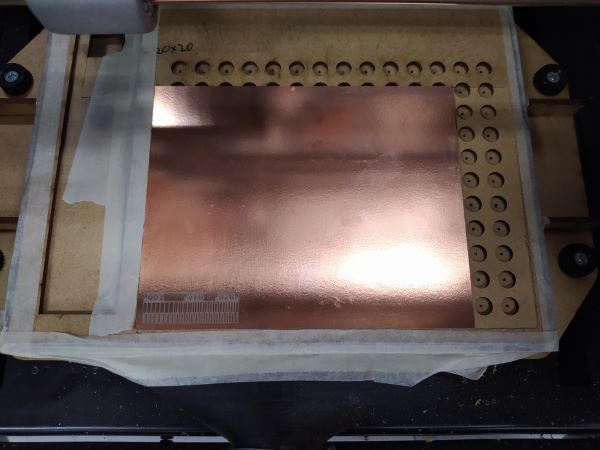
I used my vacuum table prototype to hold the PCB for the milling operation. I set the Z-height by gently dropping the tool on top of the PCB and tightening the collet. This process is also described above. I loaded the RML file to VPanel and started cutting.
Vacuum table prototype
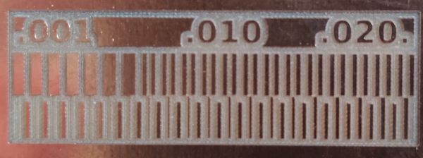
The linetest is in inches so the first usable trace was 0.007 inches so in metric it would be 0.178mm. The first succesful clearance was 0.008 so 0.203mm.
Linetest results
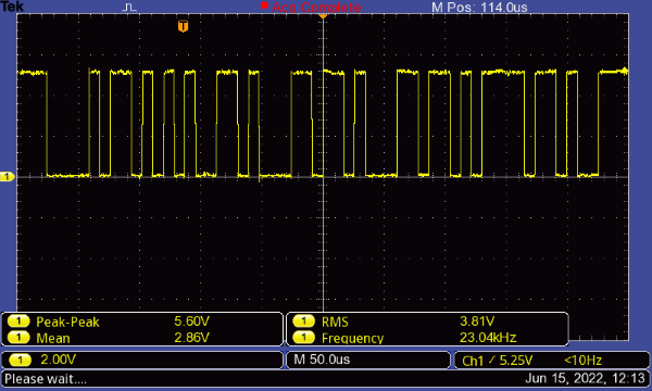
I used oscilloscope to measure ATtiny412 echohello boards UART transit line. I was just sending it a's and it was responding with" hello.t412.echo: you typed "a"".
ATtiny412 RX line
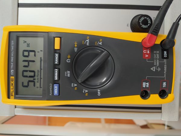
I measured the ATtiny412 echohello boards voltage wiht multimeter. It was 5.049V.
ATtiny412 RX line
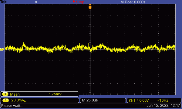
I used the AC coupling to check the ripple in the voltage. Ripple was really small.
Ripple
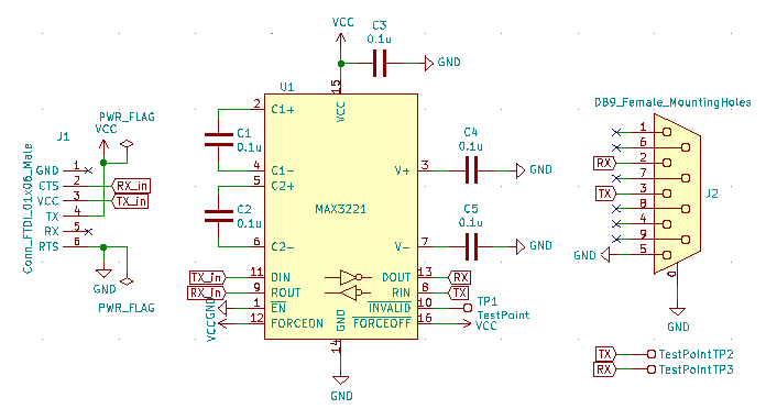
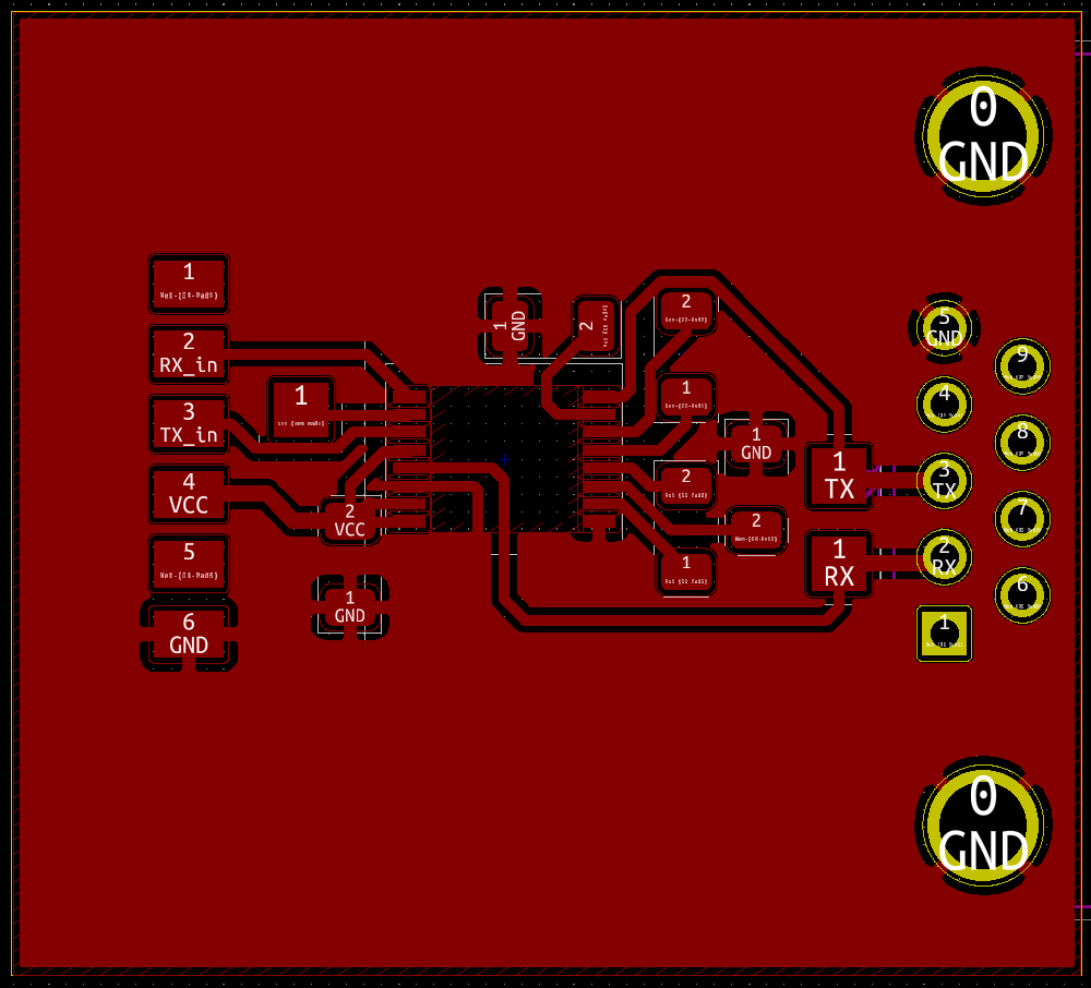
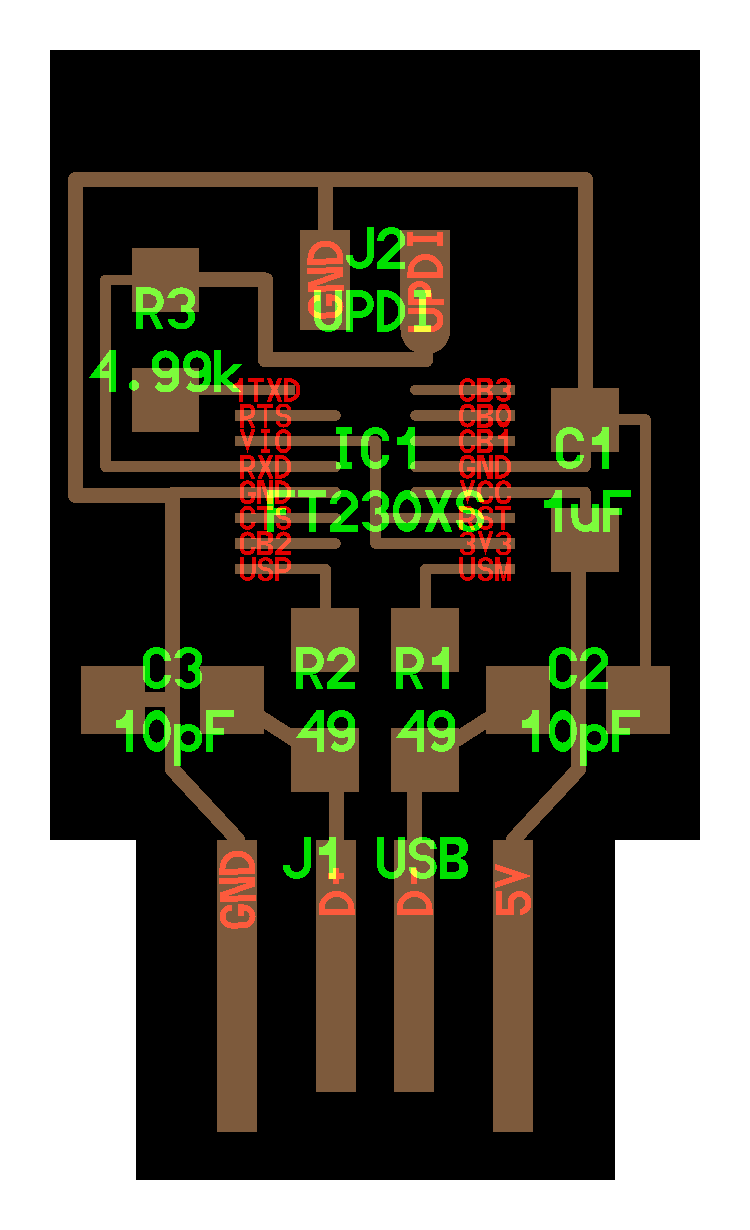
I had designed and manuafactured a quick FTDI to RS-232 board so I could quickly test if my final project was going to work at all.
FTDI to RS-232 schemaFTDI to RS-232 PCB
There wasn't much to it. I used MAX3221EAE and used the information from the datasheet to configure it to stay always on. A nice design feature of this chip is that it only needs 0.1 µF capacitors so assembly is really hard to mess up. I put some test points on the board so I could probe or attach bodge wires more easily. Agilent 54622D user manual has the DB9 pin out on page 6-10.
First schematic
- boot select and enable delay from datasheet
- Memory card pins from ESP32 GRBL board. Memory card is just future proofing or extra at this point but since it took so little to implement it I put it on the schematic
- I wanted to use headphone jack for the external button
- Barrel jack for power since I'm taking the power straight from the oscilloscopes printer power output
- Even though both of them are in the Fab Lab inventory, they weren't in Fab electronics component library for KiCad
- I dowloaded and installed snapEDA plugin for KiCad and downloaded the jacks from there
- I'm pretty sure that the snapEDA plugin messed up my paths so I had to manually set them again
- Now I'm just hoping that I got all the six TX and RX the right way
Horizontal PCB directly on the connector
My idea was to make the PCB horizontal so it wouldn't stick behind the oscilloscope. I made couple of iterations of the PCB but I just wasn't happy with it. I also worried about how could I model the case to be sturdy enough around the connector and would my skills at modeling be enough to do that?
Because those reasons I decided to change the whole design. I would just make a rectangular PCB with wires and connectors and case would just be a box. This meant that I had to redesign the PCB but case design would be much easier and I could catch up with my schedule.
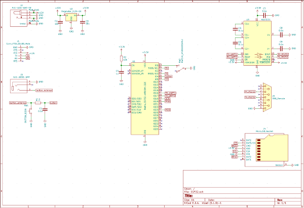
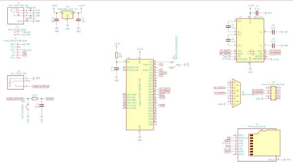
Second schematic
I added 2x5 pin header to the schematic because I was going to use a flat cable to connect to the DB9 connector. I still left the DB9 connector to the schematic so that it would be easier for me to keep track of the TX and RX pins. I also added a pin connector for the power.
Second schematic without copper fills visible
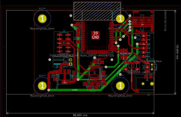
There was this indentation in the back of the oscilloscope that I wanted the device to fit in. So I laid out some guide lines to limit the size of the PCB according to my measurements. I made it double sided just so I could get away a bit easier in the design phase and I know that the LPKF is totally capable of doing this. Based on my and Joni Skofelts test over the summer, a good via size for hand soldering was a 0.6 mm hole with a 1.5 mm pad so I used that size. I wanted the SD-card and the external button connector to the right side so they could be easily accessed and power and DB9 to the left because that is the direction that those connectors will be coming.
While milling the board I had two problems. First was that I messed something up and the "plated holes" weren't drilled at all. I was bit distracted and noticed this only after fully removing the board so I couldn't fix it anymore. Second problem was that someone had closed the menu that allows you to jog the machine. This meant that when it was time to flip the board and locate the ficiduals I couldn't jog the machine to locate those. The program didn't allow me to turn that menu on during machining so I had to abort the whole process.
I milled the second board and that went smoothly. I used unplated mounting holes in the PCB desing and that caused a bit of a wierd tool path while milling. First the holes were drilled and then milled to the correct size. After that when the end mill was used to clear bigger areas from the copper, it also milled over the mounting holes. Which meant that the machine was just milling the air since the holes were already there.
MAX3221 and some of the vias soldered
I started the assembly with MAX3221 since it is the hardest part to solder. While soldering these small IC's I wish that I had slightly smaller diameter solder so I didn't flood everything with solder. AFter that I started to solder the vias since Fab Lab itself doesn't have equipment for making real plated holes or vias. I used one wire from a flat cable because it is small and multicore so it sucks solder well with capillary action.
I left the SD card socket and button unpopulated. When it was time to solder the SD card socket I had already returned the flux to the Fab Lab and the Fab Lab was closed. With the button I thought that I wouldn't use the on board button anyways so I left it out. I also soldered just the ground pin of the FTDI-header because if I wouldn't mess up the boot.py file I could update the program through WebREPL after the first programming.
Programming the board
I had done a quick beeper test with multimeter and tested that the ground and none of the power lines were shorted. I also tested some of the data lines for continuity.
I powered the board first time at home and I don't have a current limited power source but noticed that the regulator was getting quite warm. So I plugged a current meter between the power source and the board. It was consuming something like 350 mA. Which was ~100 mA more than I was expecting but not crazy amounts. While doing visual and touch testing I noticed that the MAX3221 IC was hot.
One capacitor shorted to ground
I focused my efforts near MAX3221 and found that one capacitor was shorted to ground through a small blob of solder. That was easily fixed with just a touch with soldering iron. I didn't measure the current consumption after the fix but nothing was getting hot anymore so I took that as sign of succesful fix. Later when testing I found out that luckily the short hadn't broken anything.

 Then I moved the Z-axis close to the blank. After that I held the milling bit with one hand and loosened the chuck with other hand. Then I gently lowered the bit so it touched the surface of the blank. I set the Z-axis origin and after that I raised it 0.2 mm. The cut depth in MODS was set to 0.1016 mm so this was too high but it is better to be too high than too low. Then with the
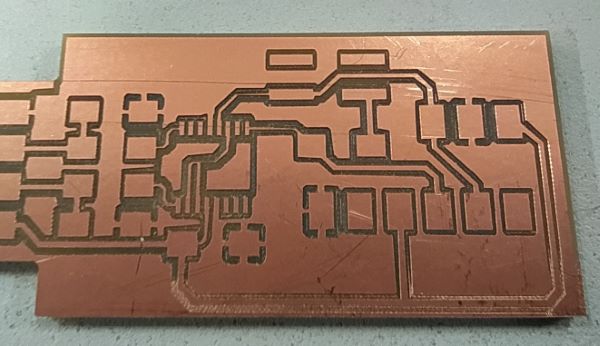