4. Electronics production
This week I learned about electronics production.
4.0 Assignment of this week
4.0.1 Group assignment
Characterize the design rules for in-house PCB production process.
Extra credit: Send a PCB out to a board house.
4.0.2 Individual assignment
Make an in-circuit programmer that includes a microcontroller.
Extra credit: Customize the design, mill and stuff the PCB and test it to verify that it works
Extra credit: Try other PCB processes
4.1 PCB fabrication
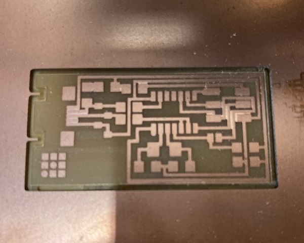
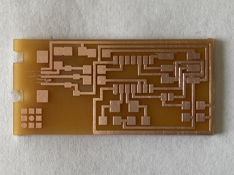
I made PCB boards for FabISP with milling machine. FabISP is a programmer for AVR microcontrollers.
4.1.1 Design rules for in-house PCB production by CNC mill(as group assignment)
Usually, PCB production process may start from circuit design and then pattern design.
Special softwares like Eagle or KiCAD are often used to design circuit patterns and Gerver files are their output.
I’m not famiiiar with these softwares yet at present, so I decided to use existing templates.
(I installed KiCAD for learning later)
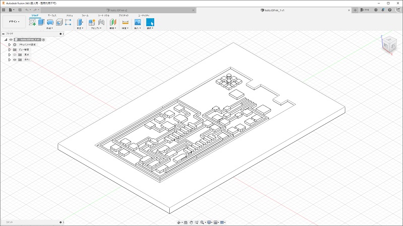
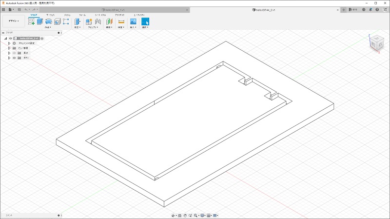
![]()
![]()
There are various ways for in-house PCB production. One of them is CNC milling.
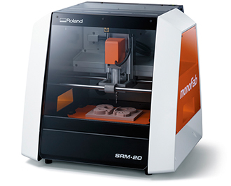
‘Roland SRM-20’ is one of the CNC mills in our lab. It is handy in size for PCB cutting. It uses the special milling software called ‘SRP Player’.
‘SRP Player’ uses STL(.stl) files as data source and convert them to special codes which are sent to the machine and used for milling jobs.
Technical data of SRM-20
| Cuttable Material | Modeling Wax, Chemical Wood, Foam, Acrylic, Poly acetate, ABS, PC board |
| X, Y, and Z Operation Strokes | 203.2 (X) x 152.4 (Y) x 60.5 (Z) mm |
| Workpiece table size | 232.2 (X) x 156.6 (Y) mm |
| Distance From Collet Tip to Table | 130.75mm Maximum |
| Operating Speed | 6 – 1800 mm/min |
| Spindle Rotation Speed | Adjustable 3000 – 7000 rpm |
| Cutting Tool Chuck | Collet method, adjustable up to 6 mm diameter |
| Control Command Sets | RML-1, NC code |
4.1.1.1 Data conversion
I choosed FabISP for the assigmnents of this week.
We can find a detailed description of FabISP in FabISP assembly tutorial. The tutorial is very comprehensive and really useful.
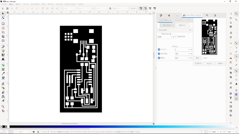
I downloaded a image file of FabISP circuit pattern from the tutorial and opened it by Inkscape.
I converted the image to vector data(called ‘pass’ in Inkscape) using ‘Trace bitmap’ funtion, and exported it as a SVG(.svg) file which can be handled with 3D-CAD softwares.
Data files:
hello.ISP.44.traces.png
hello.ISP.44.svg
4.1.1.2 Local design rules for CNC milling in our lab
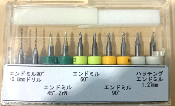
We have several end mills with various sizes and shapes in our lab.
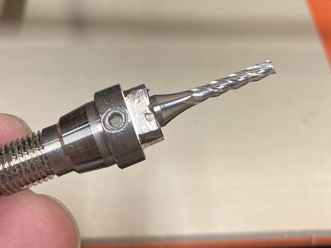
Among them, I used 45 degrees conical mill for engraving ciruit pattern, 0.8 mm flat mill for cutting, and 3 mm flat mill for planing a waste board.
So I should consider the character of these mills for designing STL data.
45 degrees conical mill is good for engraving sharp pattern, but engrave depth shouldn’t be too much, otherwise mill hits side walls of the pattern.
0.8 mm flat mill is used for cutting, so cutting lines should be designed wider than the diameter of the mill.
3 mm flat mill or wider ones could be used for planing a waste board.
4.1.1.3 Creating STL data:
I imported the SVG data to Fusion 360.
I added the depth to the pattern and made a couple of STL files. One is for engraving and the other is for cutting.
Reflecting on the local rule described above, engraving depth were defined as 0.45 mm (thickness of copper-clad is said to be 0.1 mm).
Width of cutting lines were defined as 1 mm.
Data files:
hello.ISP.44_1.stl
hello.ISP.44_2.stl
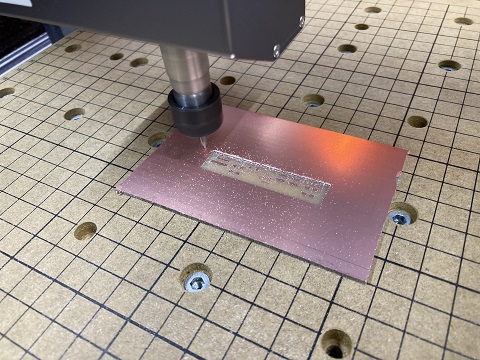
4.1.2 Cutting patterns by CNC mill
4.1.2.1 Material
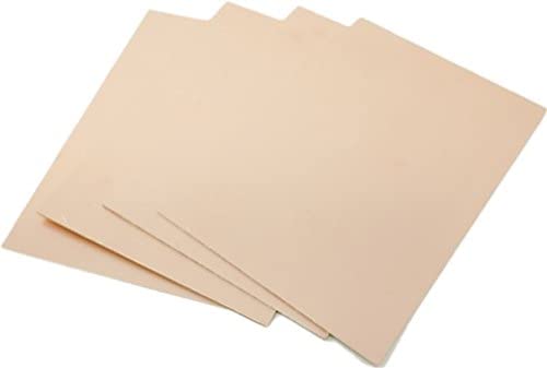
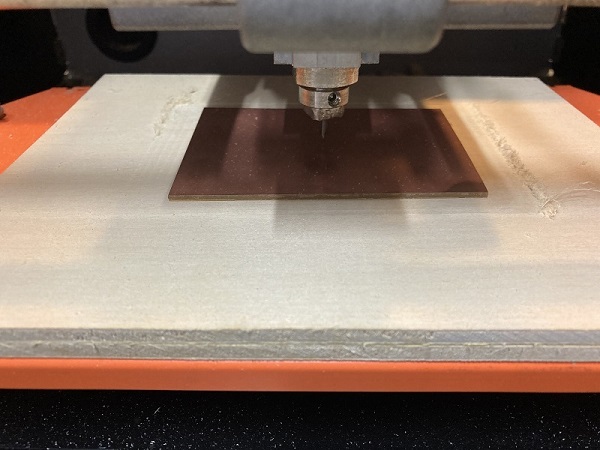
I used a 1.6 mm thickness laminate board with 0.1 mm thickness copper-clad(FR1) for a PCB and a 5 mm thickness wood panel for a waste board.
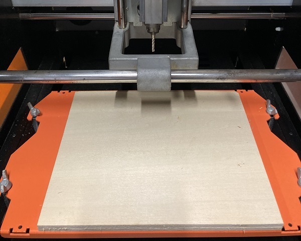
The waste board was fastend to the work bench by double-sided tape.
4.1.2.2 Set up
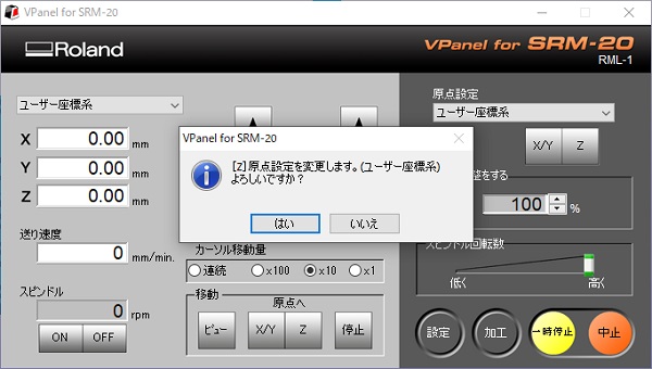
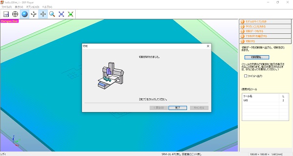
‘VPanel’ is a control interface of ‘SRM-20’. Screenshot shows the origin decision of the machine.
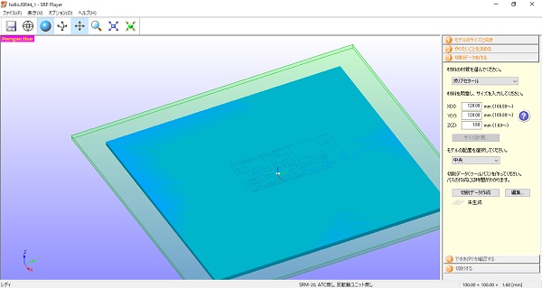
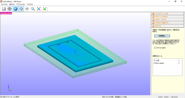
The STL files imported to ‘SRP Player’.
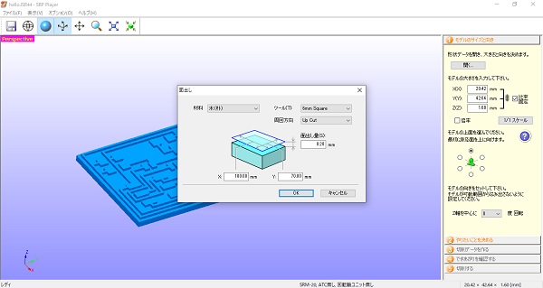
Various parameter settings. Screenshot shows the work size of a waste board defined as 120 (X) x 120 (Y) x 1.6 (Z) mm.
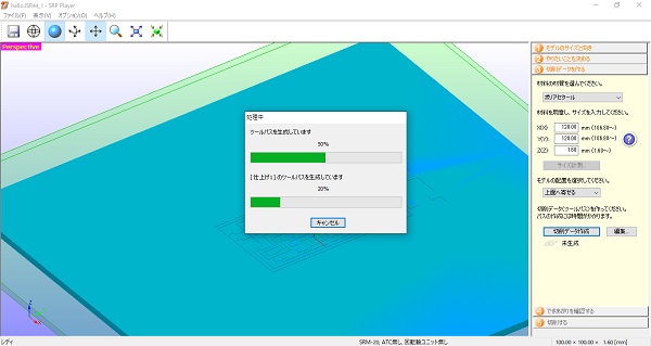
Creating the tool path for planing.
Planing the top surface of the waste board.
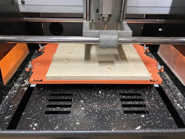
4.1.2.3 Milling
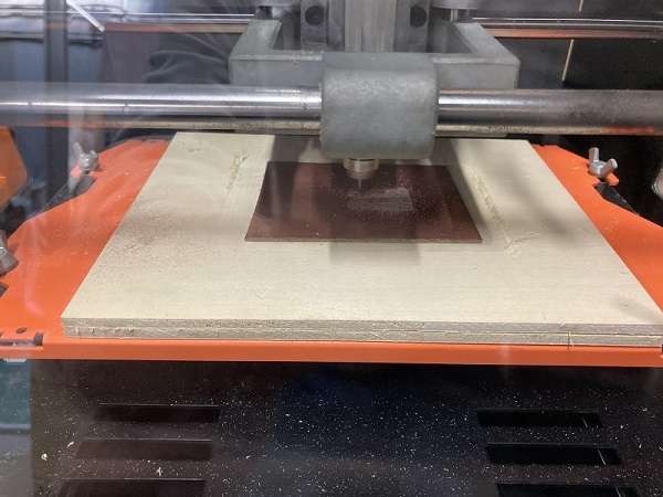
The copper-clad laminate board was fastend on the waste board by double-sided tape.
Set the end mill for engraving.
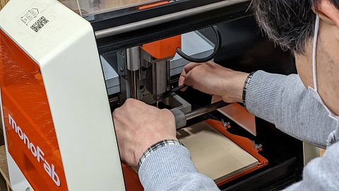
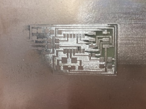
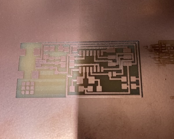
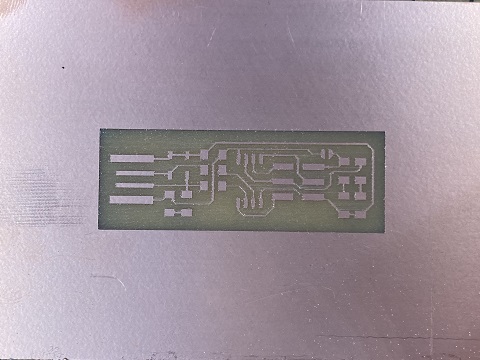
Milling the circuit pattern.
The first trial was failed. The work wasn’t set precisely and the cut result was uneven.
Retry finished.
The second trial resulted good!
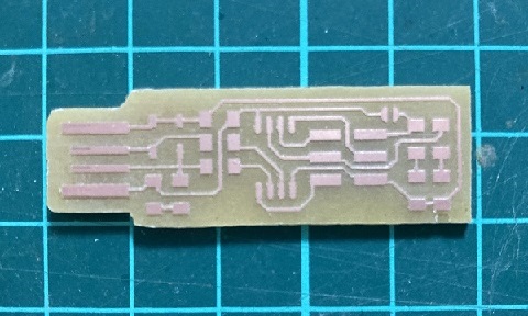
Loading the cutting data.
Cutting four sides.
The result seemed good at first.
But I found several mis-cuts through close inspection.
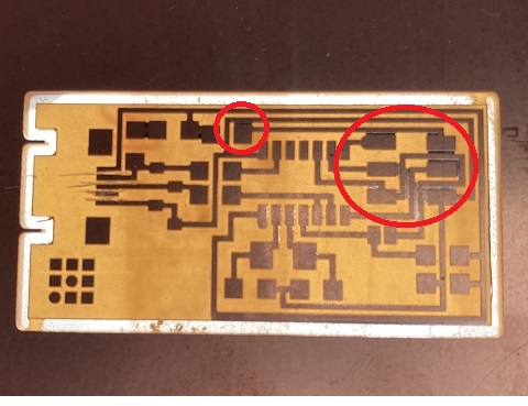
I fixed them by cutting grooves through.
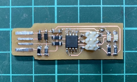
4.1.3 Making of an in-circuit programmer
4.1.3.1 Tools
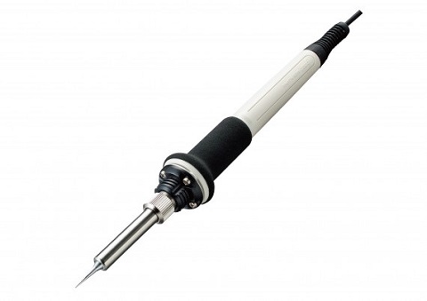
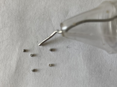
I used a 20 W soldering iron with a fine tip and 1.0 mm diameter solder wire(lead free) with melting temperature 183 - 190 degrees(Celsius).

I was advised from my tutor that solder wire should be cut into small chips for mounting small parts. I tried it and it was really convenient!
4.1.3.2 Parts
Parts list of FabISP is shown in FabISP assembly tutorial.
Currently, stocks of electronics components are very low worldwide and it is very hard to get them. So I should recycle several parts from old samples.
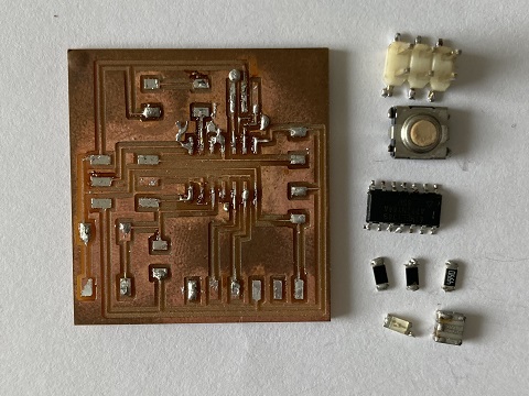
4.1.3.3 Assembly
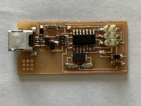
I solderd various chip components on the engraved circuit board to make an in-circuit programmer.
I would like to try solder paste and a heat gun method next time.
4.2 Programming of the board
4.2.1 Programs, drivers and writer etc
Several programs and drivers should be installed to my PC in order to activate the in-circuit programmer.
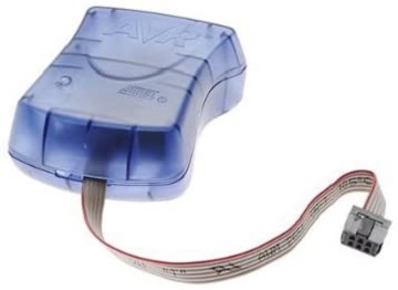
Also a hardware called ‘AVRISP Mk2’ is necessary for writing a firmware to the mirocontroler in order to make the board work as an in-circuit programmer.
4.2.2 Activation steps
The activation steps of FabISP are described in FabISP assembly tutorial
According to the tutorial, I tried the following steps but haven’t succeeded yet.
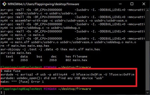
The screenshot shows that ‘make fuse’ command failed because program couldn’t find any USB devices.
Rico-san of FabLab KAMAKURA kindly advised me on the regional review session that it might be device driver issues which often occur on Windows PCs.
I am working on the issues, though not been fixed yet, but I learned from internet search that many people have suffered from similar problems. So I believe that I would be able to fix the trouble finally.
4.3 Making of an in-circuit programmer (Part2)
I had a trouble with FabISP and it didn’t seem to be solved easily, so I decided to suspend the project and try another one. FabTinyISP was my second choice.
As to FabTinyISP, Academy tutorial was helpful to understand the architecture and preparation/activation steps.
4.3.1 Parts preparation and assembly
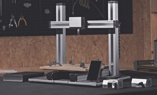
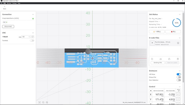
Parts preparation went quite smoothly. I used ‘Snapmaker 2.0’, the third CNC mill in our lab introduced last year, for engraving the board.
Luban, the excusive software for ‘Snapmaker 2.0, was used to slice the data and to control the machine.
4.3.2 Programming of the board (Part2)
4.3.2.1 Compiing firmware
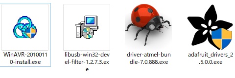
According to the tutorial, I installed several programs and drivers to my PC in order to activate the in-circuit programmer. I used ‘AVRISP Mk2’ as a programmer, so I edited the makefile of the firmware and compiled the related codes into a hex file.
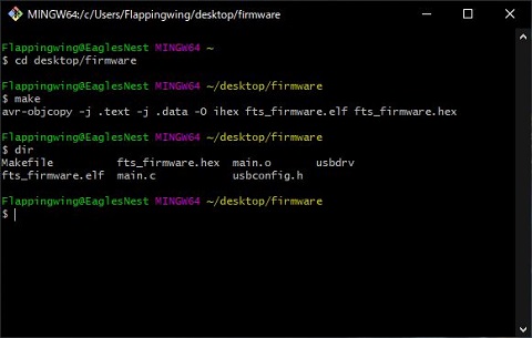
Hex file:
fts_firmware.hex
4.3.2.2 Writinng firmware
I connected the board to ‘AVRISP Mk2’ and ran ‘make flash’ command from Bash console. It worked well and the firmware was successfully written to the board.
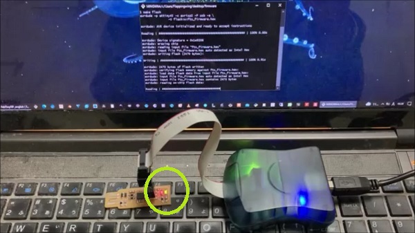
The green LED on the board flashed for a short period during writing process.
4.3.2.3 Activation
I will soon activate the board as an in-circuit programmer in the next days…