Week 4: Electronics Production
Goals for Electronics Production
- Practice Soldering
- Mill, stuff and program a working ATtiny412 Blinkie board
- Mill, stuff and program a working custom Blinkie board
- Mill, stuff and program a working Programmer board
- Characterize machine as a part of group project
- ~ Begin refreshing myself on electronics 101 in prep for future weeks ~
- Group: Characterize the Bantam PCB milling machines
~ are stretch goals ~
Some Solder Practice
I began by watching a few guides including the solder bootcamp and this one here about clearning the iron tip. Note, according to this last video, lead solder is a hazmat material and should be disposed of accordingly.
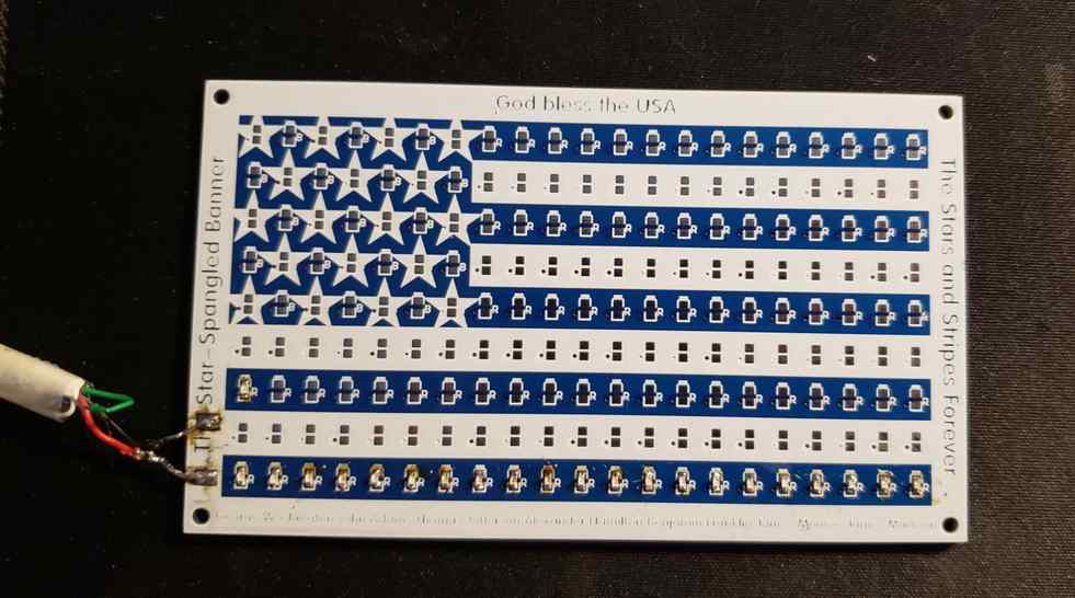
Then I turned my attention to our solder practice excercise, the American flag kit.
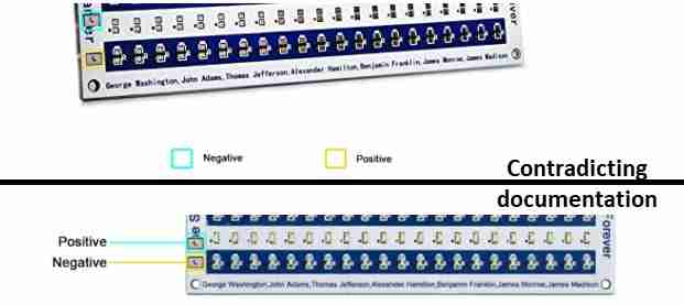
The board came with no instructions and is poorly labled, so I had to think through a few questions and answers.
- Which side of the LED is pos/neg?
From looking at the documentation on similar LED’s, it seems that the horizontal bar of the green T will refer to the anode (+) whereas the vertical part of the T will refer to the cathode (-). Similarly, on the topside, the green dot refers to the cathode side (-).
- Which side of each LED position on board is pos/neg?
From the Amazon Q&A:

- Which side of the power inputs is pos/neg?
Unfortunately the kit page contradicts itself on this point, so I will try both:
- How much power?
From the Amazon Q&A:

For power, I stripped an old micro-USB cable which had 4 internal wires colored red, black, green, and white. Unless proven otherwise, I will assume that this cable follows the industry standards and red is (+5V), black is ground (-), and green/white are related to data transfer.
So I started off by soldering a row of LED’s and the power leads. Unfortunately, I did not have any LED’s lighting up. My first attempts at troubleshooting were as follows:
- Reversing the input power to account for contradicting documentation
- Testing a wall outlet instead of running the power through my PC usb
- Flipping LED's in case I misunderstood documentation
To no avail. After asking the group, it turns out the kit comes with a strip of resistors to be soldered onto the backside of the board. At this point, I’m thinking duh. After soldering on a row of these (no polarity), it works!
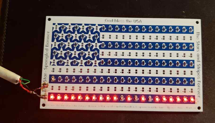
Good enough for practice I figure, it was time to move on.
Making a Blinke from an ATtiny412
Soldering the 412
With the class, we aimed to mill, stuff, and program custom ATtiny 412 boards. We we’re following this guide here.
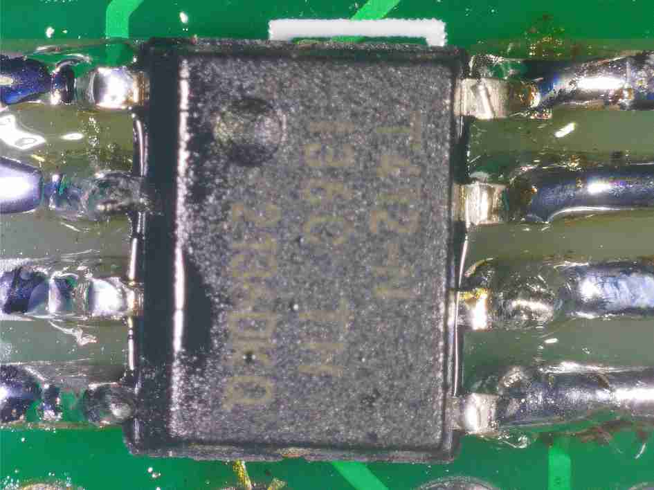
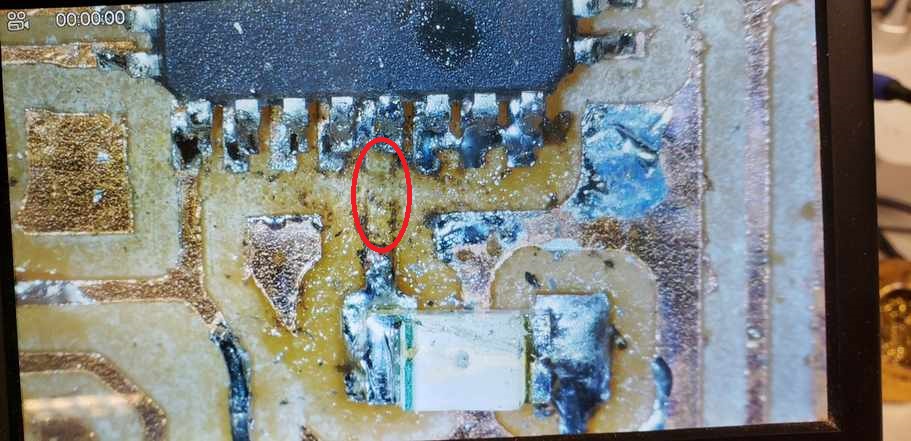
This is basically as simple as a board gets. It is a “breakout-board” which allows the ATtiny412 chip to talk to a breadboard. Steps we took to make this board: - Through-hole soldered header pins to the breakout board using a taped down breadboard to brace everything in place. - Surface mount soldered the tiny412 chip to the breakout board at all 8 pins - Verified solder joints using the magnifier station. Snapped photos and transferred them to laptop via microSD
Setting Arduino as UPDI Programmer
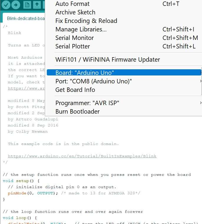
When it came time to program this board, we used the megaTinyCore program to program one of these new ATtiny microcontrollers using the Arduino IDE. To transfer the program to the chip, we used an ardunio uno as a UPDI to program the 412 chip. In other words, the Arduino was setup like a bootloader to program other chips.
To setup the Arduino as a programmer, we needed to import the jtag-2-UPDI library into the Arduino IDE. Originally, we attempted to do this by using Sketch - > Include library -> Add Zip Library to launch the downloaded package into the IDE program. Tom mentioned this worked best in past years. That being said, we were unable to locate the jtag2UPDI.ino through the IDE software using this method. After some poking around, we found the best method was to actually first unzip the package jtag2UPDI-master.zip, and then remove “-master” from the unzipped folder.
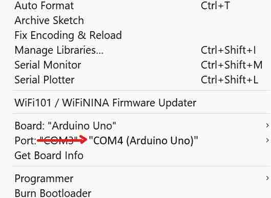
Then we simply opened the jtag2UPDI.ino in the IDE program and uploaded it to the ardunio uno, being sure to set the Board and Port correctly. This lined up more closely with the guide. That being said, there was some troubleshooting involved here as well. We found that the original board we we’re working with (sparkfun redboard) did not want to accept the code. We we’re left with the spinny wheel of death after hitting upload. After switching to an ELEGOO Uno, the code successfully uploaded. The only other change that could have had an effect here, was that the Port option switched from COM3 to COM4 (Arduino Uno). This worked because the computer was recognizing the new board as an UNO.
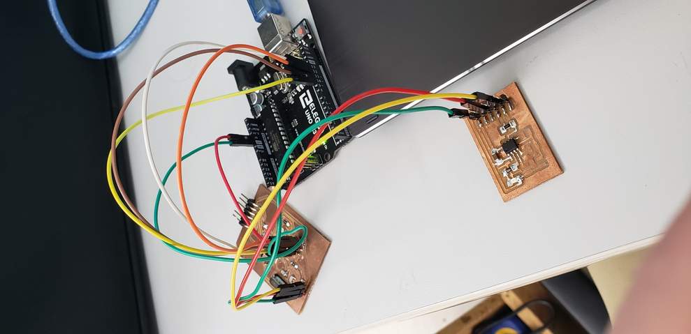
Its worth noting that at this point, we had the entire circuit setup and ready to program the 412 board (see circuit below). That said, we could’ve done this first step by simply plugging in the Arduino via USB.
Programming the 412 to Blink
To program the ATtiny412, we built the following circuit.
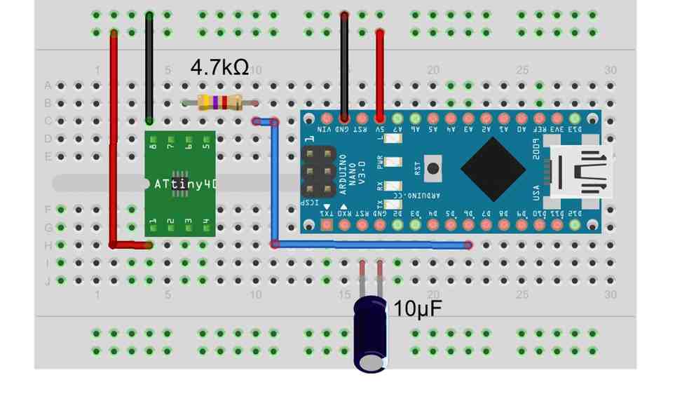
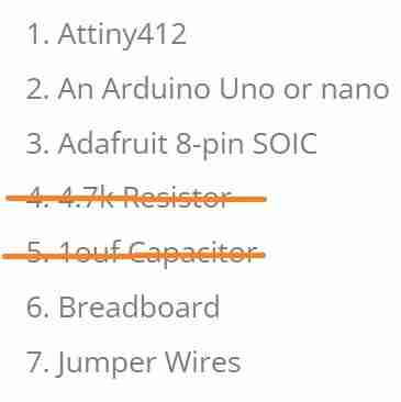
However, from experience, our team knows we can negate the resistor and the capacitor. Updated BOM:
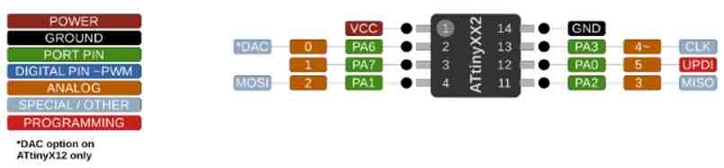
Lastly, we we’re paying close attention to the 412 pinout diagram.
In the Arduino IDE, we found the Blinkie program from examples - > basics -> blink.
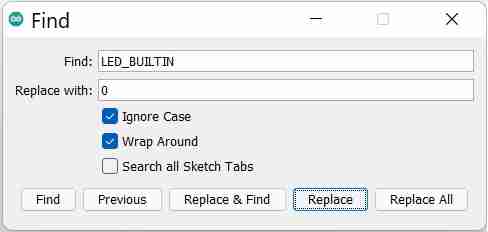
The program was ready to go for us aside from one key change, which was to change the variable “builtin” to “0” so that we could control the LED attached to port 0 on the AT412 board. This replacement was easily done by using IDE’s find/replace function (cntrl-F).
From there, we we’re able to load the blink demo onto the 412 board using the Arduino as a programmer. The program was sent through the UPDI port on the Arduino (6) to the UPDI port on the 412 (5). At this point, the LED began to blink successfully!
It is important to note that the entire setup was still running off of the USB power connected to the PC. At this point, I got a little ambitious and wanted to see if the setup would run off of a 9V battery. I promptly hooked it up and found that the setup did run successfully as pictured below. The light blinked on and off.
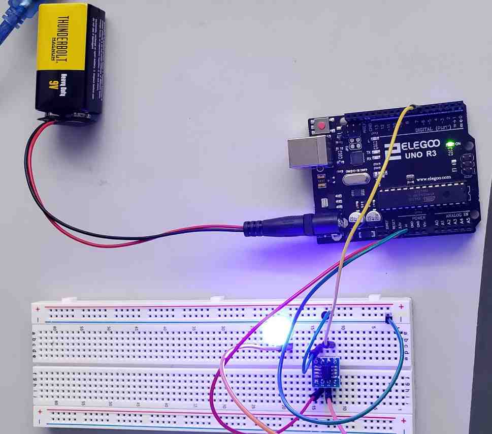
That being said, I was later informed that hooking up one of these 412 boards to a 9V without additional protection, could result in a fried board. In this case, I should consider myself lucky because I did not leave it hooked in for long and it did not appear to get fried. That being said, because I made this error, I should consider this particular 412 board as suspect going forward.
Making a Custom Blinkie
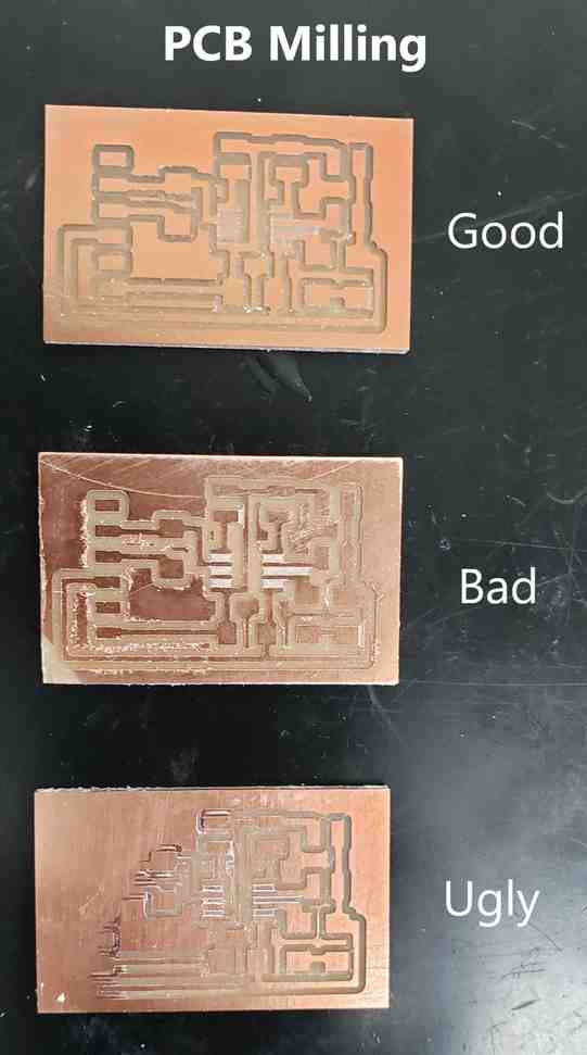
The next week, we repeated this process but instead of building the blinkie circuit off of a breadboard, we moved to an integrated blinkie board. For this step, Tom was still doing the milling for us, but we followed along to watch his process. From this process, we had mixed results and learned what makes for a good, bad, and ugly board.
Then, following along the circuit diagram, we soldered on the necissary components, being careful to not create any solder bridges.
After it was soldered, we followed the same process as the previous week to program the Arduino up as a bootloader and load the blinkie program onto the custom board. I made one key error during this process which is that I accidently programmed the Arduino as the blinkie, which led to the comical result that one of the Built-in LED’s began to blink. This was also a sign that I needed to use the adjusted Blinkie code! Anyhow, once this was worked through and the Arduino was reprogrammed as a UPDI programmer, and it blinked!
Here is a graphical representation of the code operating inside of the 412 chip:
We then verified our success by changing the time intervals and resending the code.
void loop() {
  digitalWrite(0, HIGH);   // turn the LED off (HIGH is the voltage level)
  delay(3000);                       // wait for 3 seconds with the LED off
  digitalWrite(0, LOW);    // turn the LED on by making the voltage LOW
  delay(1000);                       // wait for a second
Noting that with this circuit design, the LED turns on when the 0 pin is set to LOW.
Making ATtiny 412 Custom Programmer
Notice: This project was eventually abandonded in favor of the SAMD board, detailed below.
The natural evolution of this work was to now replace the Arduino with a minimal UPDI board that uses AT Tiny Mega, and is dedicated to being a programmer. In Neil’s words,
“Arduinos are actually 5 or 6 different things” - Neil
Thats when it all began to click for me, and I understood that having a board dedicated to programming other boards will be useful. It also fufills our individual assignment for the week, so we’re finally into the meat of it!
To do this, we we’re following along on Adam Harris’ gitlab page, which has since been taken down. For this process, I was working alongside my sister Avery.
Milling
We are following our Fablab’s published workflow for the Bantam machines.
We downloaded the .brd file from gitlab, and opened it up in the Bantam printer driver. This board uses two different tools, the 0.005” degree engraver and the 1/32nd flat-end-mill. Here we learned the process of swapping out tools and touching them off, which the software does automatically after a tool-change.
We then taped down the stock (FR-1 sheets of copper) to the spoil board using double sided Nitto tape. At this point, we want to use the Bitbreaker function to probe the thickness of the stock. At first, this returned an error and could not find the stock. At this point, a team-member informed us that the little clip on the side of the machine table needs to touch the stock. This completes a circuit (for conductive stock only), and tells the software when the bit is touching the stock.
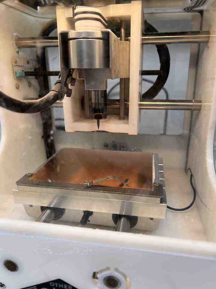
After these two probing processes, our software understands the length of the tool and the thickness of the stock.
Looking at the program view, I was told that if you see red, you have a problem. It means that you haven’t accounted for all of the tool paths and may need to select another tool. By inputing the 0.005” engraver, and hiding the other features (wider traces and cutaway lines), we we’re able to get rid of all of the red, and begin to engrave.
Similarly, once this process is done, we * swapped the tool for the 1/32” FEM, and let it reprobe * Hid the engrave features and marked the traces/cutaway as showing * Closed the machine and hit cut
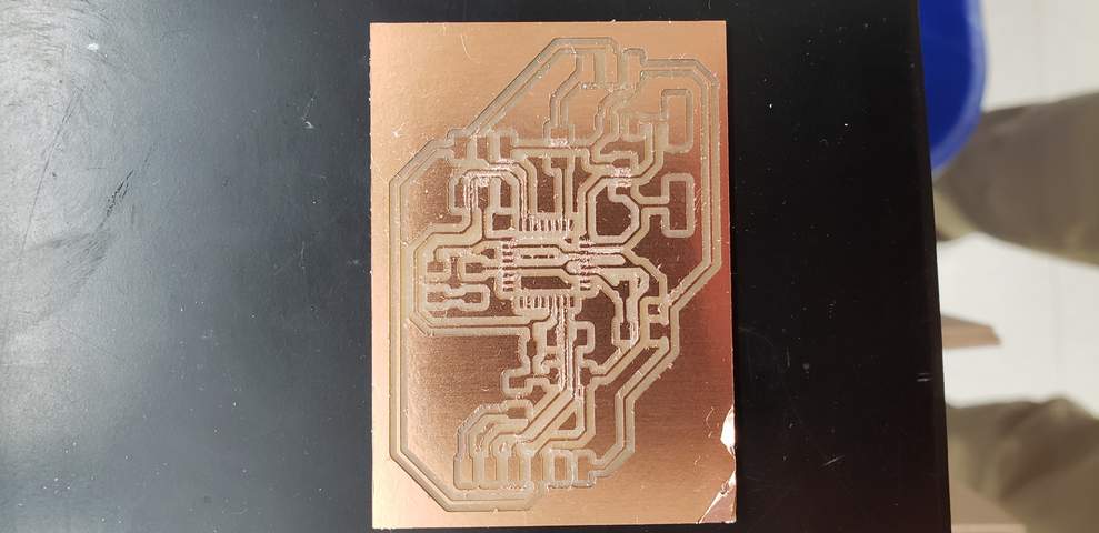
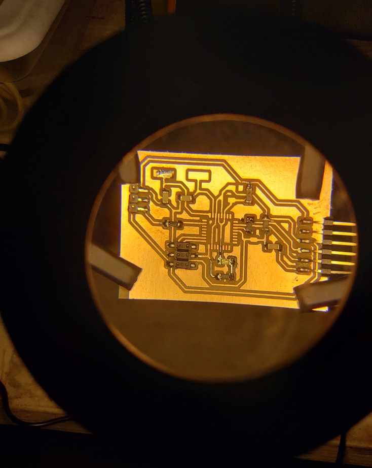
Here is the result.
Soldering
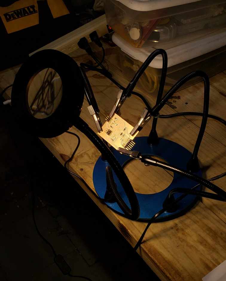
My first board was going well, but I made a critical error. Despite others’ advice, I saved the smallest and most critical component for last, the AtMega328p chip. After succesfully attaching this with the drag soldering technique, I noticed a 2nd mistake. I soldered the chip on in the wrong orientation. In comes my 3rd mistake… rather than being patient and waiting a few days to remove the chip properly with a heat gun, I grew impatient and attempted it with tweezers. The chip came off, but with it came a critical trace leading to the LED.
Following the same process, I milled a 2nd board with no major problems. I used a heatgun for the first time to remove components from the first board in an effort to reuse them.
The new board was then successfully soldered with no bridges and starting with the smallest/toughest components first.
Programming the Programmer
Now came time for the programming phase. Still following Adam’s lead here, I first hoped to upload blinkie to the programmer, as a proof that it is soldered correctly.
To do this, set the pin variable to 6 and the tools settings as follows.
I wired the arduino to the programmer by connecting Digital 6 to Sck. After adding power and ground, the blink program succesfully uploaded to the programmer. Question remains which chip this was running off of?
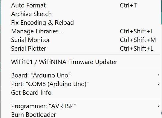
My next goal was to program the programmer with jtag2UPDI. But first, I needed to program the Arduino as an ISP.
By following the documentation here, I uploaded the example code “ArduinoISP” to the arduino with the following settings.
Once that was uploaded to the arduino, I could attempt to upload the jtag2UPDI code to the custom programmer. This was done with the following settings, and specifically setting the programmer to “Arduino as ISP”.
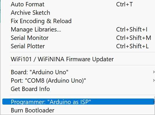
I wired the arduino using the following circuit diagram to wire the custom programmer’s ICSP pinouts. The code uploaded without error, but it is tough to verify if the jtag2UPDI code uploaded to the custom board or to the arduino.
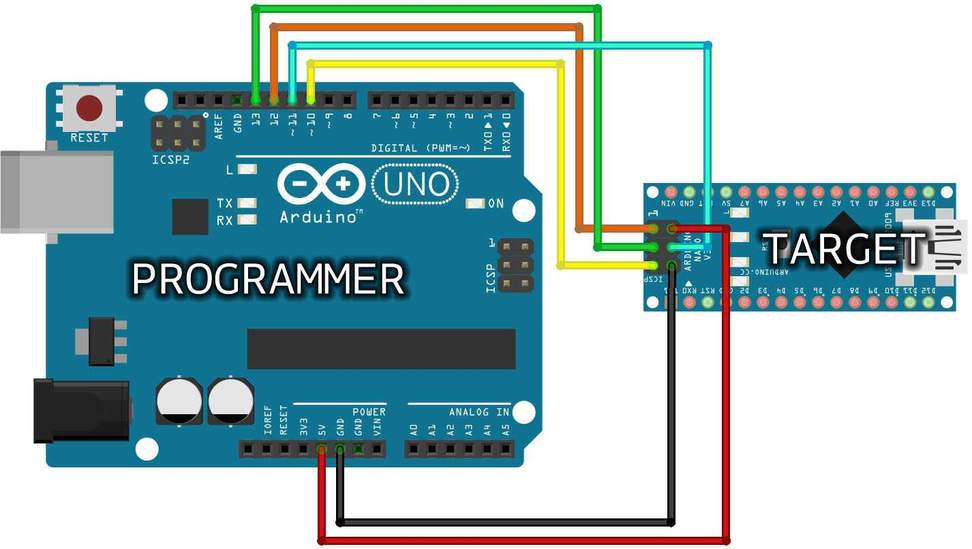
In hindsight, this diagram is intended for programming an arduino nano. While the nano and the Uno both use the 328p chip, this still may not be the correct wiring.
Attempting the next step, I was unable to program the blinkie using the custom programmer.
At this point, for reasons beyond my current understanding, the ATtiny programmer was abandoned by the entire team in favor of the newer SAMD design detailed below. This is also why the page has been taken down from sheekgeek.org. It was eventually found that the jtag2UPDI library did not play nicely with the 412 chip. We think it had something to do with baudrate. So we moved on to the SAMD design detailed below.
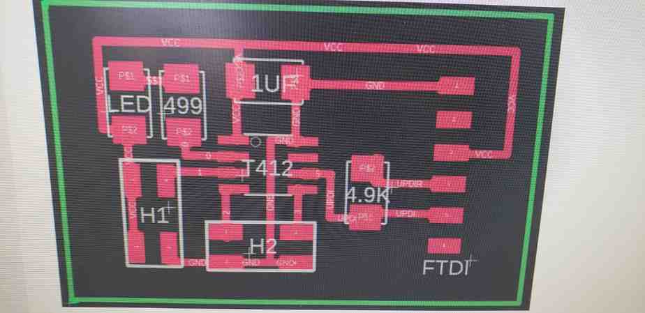
Making SAMD Custom Programmer
For this build, we are following Adam Harris’ page here which is maintained here.
Milling
The board milling process took a few iterations. To start, we attempted to use 3 bits (1/32”, 1/64”, and 0.005” engraver bit) to mill these boards.
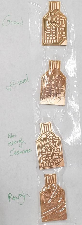
For the first attempt, the trace clearance was set too low and led to the results labeled “Not enough clearance”. Eventually, we set trace clearance to 2.0 mm and Trace Depth to 0.20 mm which led to better results.
Despite probing the center of the material correctly, one machine still led to the results labeled “off-level”. This machine was treated as suspect and we moved to another machine.
Despite fixing these issues, we were still getting rough traces and burrs around the traces. This led to the results labeled “rough”.
Eventually we found the best method was to drop the 1/32” bit entirely and only use the 1/64” and engraver bit. This led to the results labeled “Good”.
Soldering
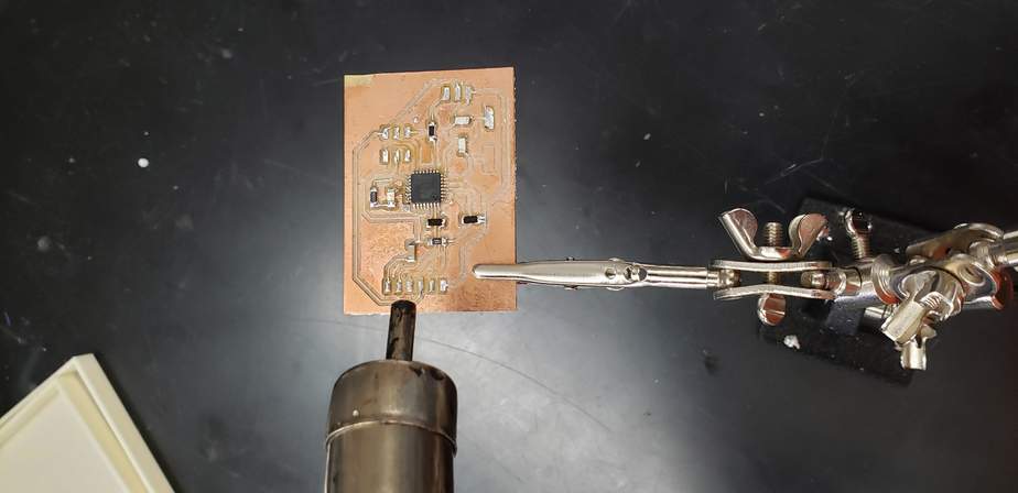
Soldering largely went off without a hitch. The only issues were in having the correct components. Originally, I pulled the wrong regulator and switch. Luckily, these issues we’re caught before the wrong components were soldered on. The results of the stuffing process are below.
Printed Housing
One cool thing about these new SAMD boards is that they are intended to plug right into a USB port. One draw back of the design is that the thickness of the FR1 board is not suitable to create a tight fit in a typical USB port. During lecture, our team was made aware that the board Adam’s board is based on, Quentin’s design, has a 3D printable housing that resolves this issue and serves as that shim. I was sent these two files which can be found in my repo here, labeled “case FabISP” and “case ftdi usb (1)”.
Adam’s design has a slightly changed profile so it was necessary to change it accordingly. I retrieved the profile of Adam’s board by downloading the KiCAD project from his repo and exported the PCB board as a STEP file. This step file was imported into Fusion and served as a basis for the design. Unfortunately, this design process took longer than anticipated and ended up taking 7 iterations to get right… a good lesson in the K.I.S.S method.
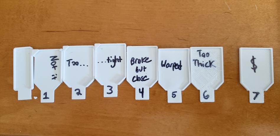
The issues with each iteration are as follows:
- Quentin’s design
- Bad Design - Board is underconstrained.
- Too tight (overhang/Z tolerances are too tight)
- Still too tight (overhang/Z tolerances are too tight)
- Z overhang broke off and I noticed it was unnecessary to hold the board in. The walls were tight enough hold the board in without the overhang. Redesigned accordingly.
- This version would’ve likely worked, but it was pulled off of the printer while the bed was still warm, and warped.
- The floor was made thicker to offer a snug fit in USB ports. It was made too thick.
- Money!
The files to produce this housing are available in my repo here.
Programming
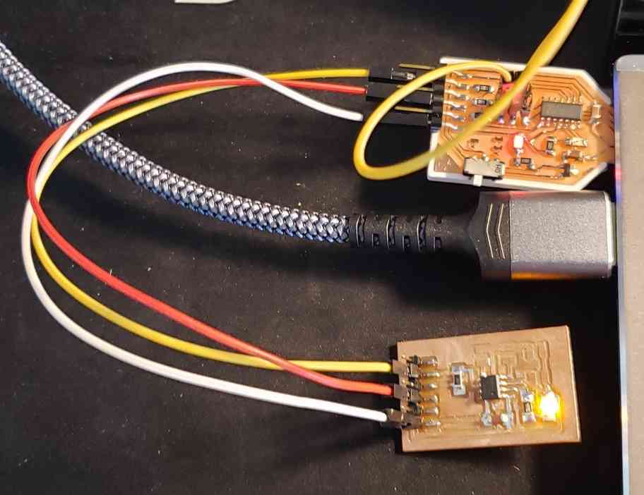
For this process, I had help from fellow classmates Nidhie and Barbara. Adam had used an atmel ICE programmer but this was not working for our group so instead we used an “ICED” SAMD board (green board). First, to load a bootloader to my new board (tan/white board), we hooked it into the ICE board in the following configuration, being sure to change all wires before plugging the boards into the computer. Also, the switch on both boards should be set to 3.3V.

We were using Barbara’s computer for this process, who had previously downloaded edbg and a SAMD11 bootloader from here. To load the bootloader, we used the following command in the command prompt.
edbg-windows-r24.exe -bpv -e -t samd11 -f sam_ba_Generic_D11C14A_SAMD11C14A.bin
edbg-windows-r32.exe -bpv -e -t samd11 -f sam_ba_Generic_D11C14A_SAMD11C14A.bin
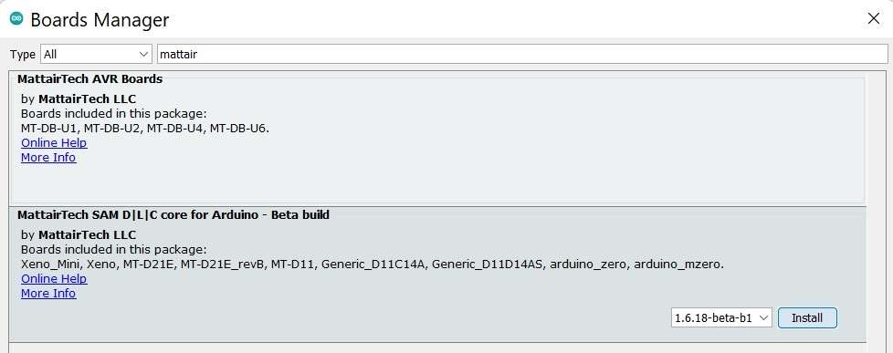
Then it was time to add the board to Arduino IDE so it could be recognized. We did this by going to File –> Preferences –> Additional Boards and adding the following link,
https://www.mattairtech.com/software/arduino/package_MattairTech_index.json
Then it could be found through the Boards Manager
After successfully loading the bootloader to my board, and adding the correct codebase to the Arduino IDE, it was time to program my board to be a programmer. To do this, we used this configuration.
To do this, we loaded the following code to my board
void setup() {

   SerialUSB.begin(0);
   Serial1.begin(57600, SERIAL_8E2); //Adjust baud rate and use SERIAL_8N1 for regular serial port usage
}

void loop() {
   if (SerialUSB.available()) {
      Serial1.write((char) SerialUSB.read()); //Send stuff from Serial port to USB
   }
   if (Serial1.available()) {
      SerialUSB.write((char) Serial1.read()); //Send stuff from USB to serial port
   }
} //end loop
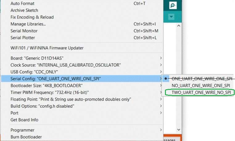
Note, the above picture has been corrected per the feedback from our global grader, Yuichi Tamiya.
After this completed, my board could now be used as a UPDI programmer.
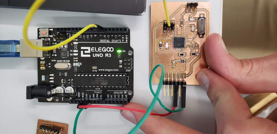
Testing the Board - Programming a target Board over UPDI
Following Adam’s instructions closely, the goal was to load a simple blinkie program to our 412 blinkie boards, which we’re made above. To do this I
- Loaded the Blinkie code used for this board.
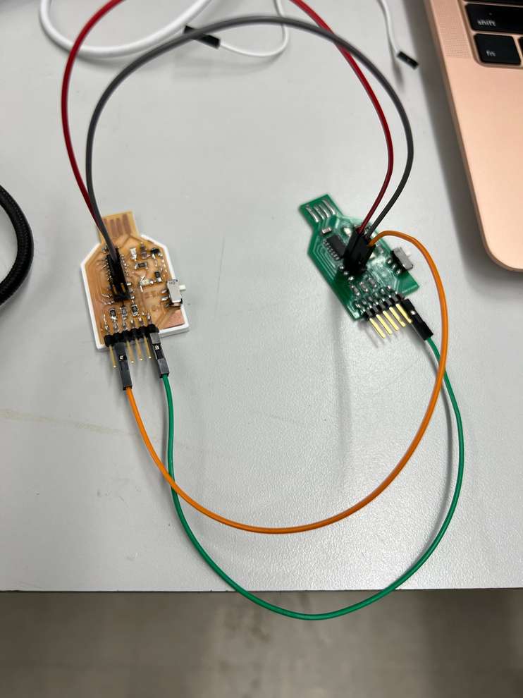
- Added a jumper wire to turn the SAMD board into a UPDI programmer (see below)
- Wired VCC, GND, and UPDI across both boards
- Switched the regulator to 5V since this is what the Blinkie board expects (noticeably brighter LED)
- Changed the chip to attiny412 to prevent reprogramming my SAMD programmer
- Changed the Programmer to SerialUPDI - SLOW 57600…
- Selected the right port and hit upload
- The Blink code updated successfully.

AVR 1614 breakout board
After talking to Neil, the ATTINY 1614 seemed like the clear choice for my final project, and inputs/outputs weeks by extension. That said, there was still much experimentation to be done in the breadboard phase so I searched around for a 1614 breakout board. I found this one by John Bradnam, however it was a little too compact for my taste. I needed a KiCAD refresher anyhow so I quickly developed a very similar board, but a little more spread out. That being said, I made sure to stick to the hole-pitch of a standard breadboard, 0.1” (2.54 mm). Luckily, the KiCAD grid is setup to this pitch by default. Here is the design, production and succseful blinking of said board.
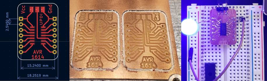
Some things I learned during this process. First, the tapered 1/64th bits did not do well at drilling the holes. As the bit got deep into the hole, the taper began to destroy the traces. Second, the long and skinny 1/64” bits that say “for drilling only”, really mean “for plunging only”. I attempted to use this to ‘drill my holes’ but the path was such that there were still significant side loads on the bit which was enough to snap it. I had much better luck with our 1/32” FEM. Upon stuffing the board, I realized that it is good to heed the notice about the horizontal headers clipping the silkscreen. Basically, the plastic part of the header needs board to rest on to avoid inducing loads on the traces. I was able to Jury rig it this time though. Also, for some reason I was only able to program this board using Jtag2UPDI so far. Not sure why the SAMD programmer was unable to program it. Possibly a COM issue.
Note, per the feedback from our global grader, we should implement capacitors between power and ground directly into our breakout boards. Here is an example he shared. This feedback is noted and will be implemented going forward.
Group Project - Characterize PCB milling machines
Documentation on our groups efforts to characterize the PCB milling machines can be found here. My contribution was to run one of the unsuccesful tests using a 1/32” bit. Our group later had success once we used a 1/64” bit.
- “Blink” is the “Hello World” of electronics
- Wash a PCB board under tap water after it comes off the mill before deeming the results good/bad.
- Use larger trace clearance (1.5 - 2.0 mm) between traces to avoid bridges.
- Probe the machine bed in multiple spots to make sure its level. For the job, probe in the middle of the desired board.
- Nearly any soldering is fixable so long as you don’t rip a trace
- The reflow gun is a great option for removing components, but always be safe.
- Shimming the USB board is better than attempting to cover the contacts with solder, which likely won’t be level
- When using the SAMD programmer to program a target, change the board/chip in the IDE to prevent reprogramming my SAMD programmer
- Adhere to the minimum trace widths and max clearances established in our group effort.
Note: All design files and images can be accessed in my git repository found here.
All works shared on this site 'A Fab Academy Journey with Charlie Horvath' by Charles W. Horvath are licensed under Attribution-NonCommercial-ShareAlike 4.0 International![]()
![]()
![]()
![]()