Week 6: Electronics Design
Goals for Electronics Design
- Finish KiCAD Tech explorations tutorials 4, 5, 8.7, and 8.8, and 9.8
- Redraw a 412 hello-world board and add an LED/button to different pins that can be controlled by software
- ~ make it expressive/interesting ~
- ~ simulate its operation before production ~
- Begin designing an MVP or proof of concept circuit board for final project
~ are stretch goals ~
Initial Learning
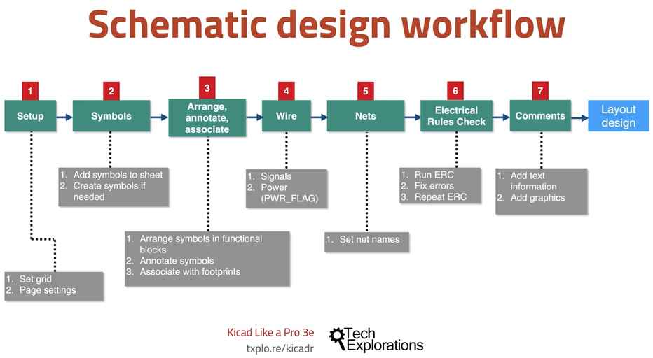
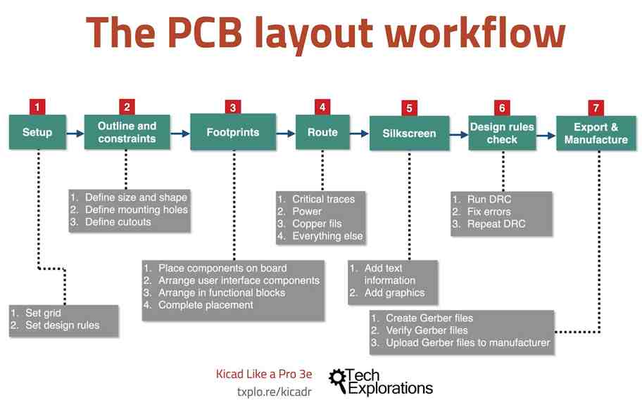
I began this week by running through a few of the tech-exploration “Learn KiCad like a Pro” tutorials (Chapters 4, 5, 8.7, and 8.8). Here I found the following detailed workflows, which I will make the basis for all the work I do in KiCad.
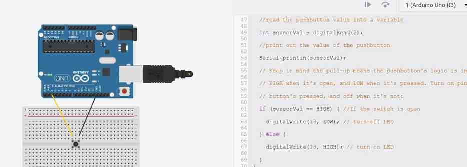
Next, I followed this example a Digital Input Pull-Up Resistor through the use of pinMode (INPUT_PULLUP). Basically, this example shows that you can control the built_in LED of the arduino using a switch on a different pin that connects to ground. Through this process, I began getting aquainted with TinkerCircuit in order to simulate the results below.
Individual Assignment - make an interactive 412 Blinkie board with Switch
KiCad - Schematic Design
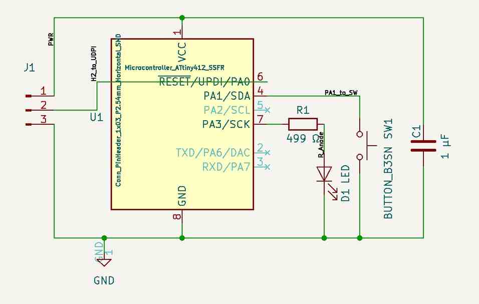
Now I moved into KiCad and attempted to draw the schematic for my interactive Blinkie from memory. My goal was to have a blinkie board that switched between blinking and fading at the press of the button. From a hardware standpoint, this only requires a blinkie board where the LED is attached to a pin that can create pulse width modulation (PWM), and the rest of the changes can be accomplished in code. First I set my grid and page settings to add information to the title block. Then I dropped in the symbols needed:
- ATTINY 412 Chip
- Decoupling Capacitor
- LED
- Resistor
- SPST NO - tactile switch
- 3x1 Header for input power/UDPI
I did the following steps slightly out of order compared to the Tech Explorations workflow, but made sure to reference it so that I did not miss any steps. I roughly arranged the components and began connecting them with traces. At this point, I decided which pins would be used for the LED and the switching. A quick look at the 412 board pinout diagram from the datasheet.
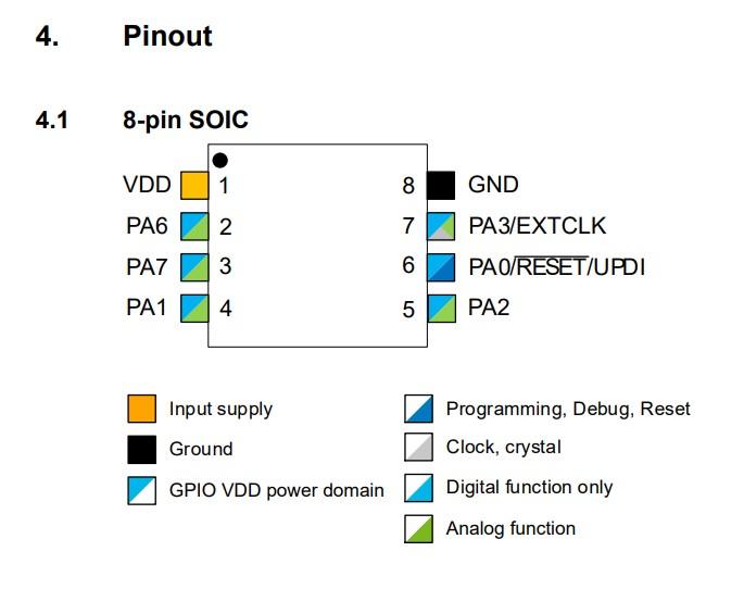
If I’m reading this correctly, then I think any of the pins labeled analog, should be able to provide PWM output. I settled on pin 7 since this pin also has access to the clock, which may prove useful. For the switch, I could pick any output pin and therefore settled on pin 4. Here was my first layout attempt.
WARNING: this schematic is not completely correct
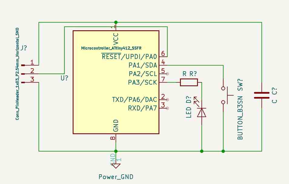 WARNING: this schematic is not completely correct
At this point, I went back and annotated the symbols and associated them with footprints. For these steps, I let the software determine the best options and simply sanity checked the results. I named some traces as practice. This excercise actually led me to realize the LED was backwards and that the anode needed to point upstream.
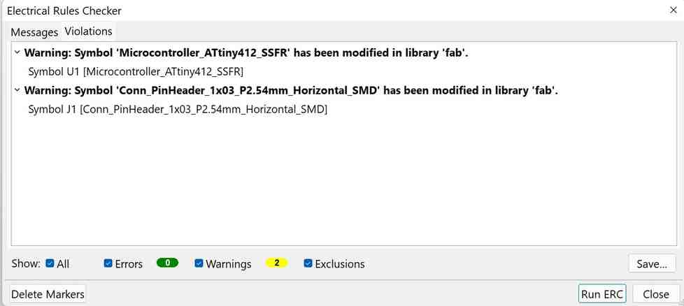
Then it came time to run the Electronic Rules Check (ERC). At this point, I received 9 errors! 7 of these errors were easily fixed by setting the unused pins as unconnected and invisible. Making these changes in the symbol editor was an important trick that Tom had shown us, see below.
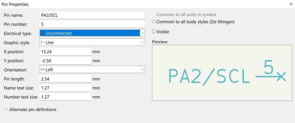
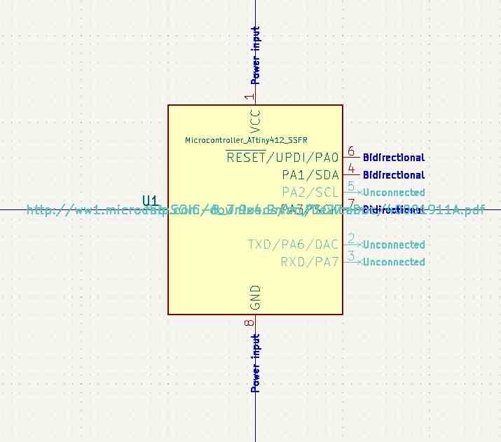
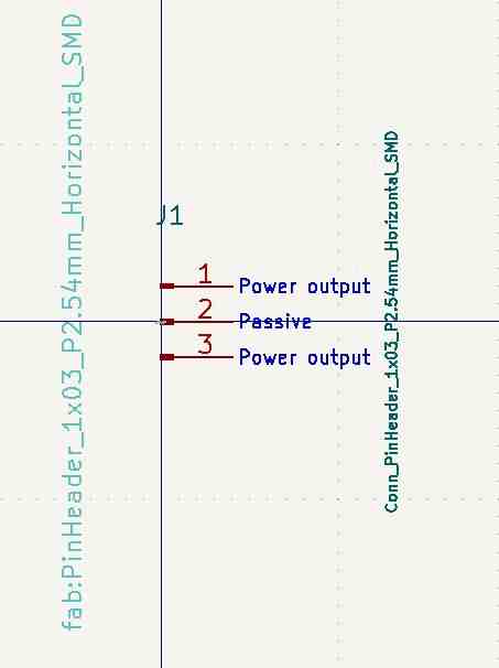
Two of the errors involved how I setup power and ground. It did not like me attaching a power flag to the input terminal. I went back and referenced Adam’s SAMD board to see how he handles power inputs/outputs. I then realized that the power header pins needed to be labeled Power Out in the symbol editor whereas the chip power input pins needed to be labeled Power In. The confusing part of this is that both PWR/GND are labeled Output and Input together as a pair. For instance, both the header pins are providing an “Output power” source to the board, and are labeled as such. I was later told that this step could also be achieved by adding power flags to these lines. However, when I attempted to add power flags, the programmed flagged it with errors… We think it was redundant.
Once these changes were made, the ERC ran off without a hitch. The only warning was appreciated, which is a reminder that these edits have been made in the symbol editor.
Here is my final schematic.
TinkerCircuit - Simulating Results
I wanted to quickly verify this circuit design in tinker circuit. Creating the Blinkie circuit on a breadboard did not take long. The only error I ran into was regarding the lines of code
Serial.begin(9600);
...
Serial.println(sensorVal);
My rough understanding is that serial is a type of communication that Arduino uses, but it is not proper to use it with the ATTINY board. By commenting these lines of code out, the issue was resolved and the board blinked successfully.
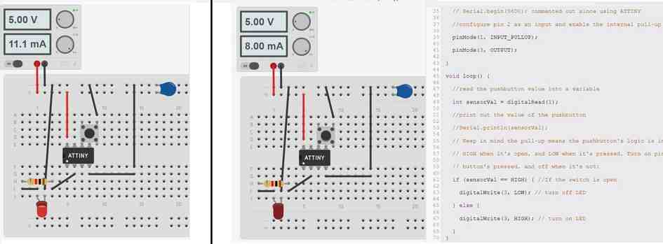
Then I began to tweak the code such that it would blink normally and then fade while the button was pressed. This was relatively simple since I simply needed to merge the blink example code with the fade example code. However, it led to unexpected results:
S
As can be seen, the output certainly changes with the button is pressed, but it is not a clean fade as expected. I am thinking there could be a few different reasons for this,
1) I tried changing both the blink and fade code to analogWrite instead of digitalWrite for the blink. Perhaps it did not like switching back and forth between analog and digital in this manner. This did not resolve the issue 2) Tinker circuit may be unable to process PWM and the fade symbol (unlikely) 3) The ATTINY chip in TinkerCircuit has different pinouts than the 412 diagram above, and perhaps the pin I am using does not support PWM
Whatever the case, I will keep thinking about this point before I get too far into my PCB production…
I later found out that Tinker circuit is not simulating a 412 but rather another ATTINY chip.
KiCad - PCB Design
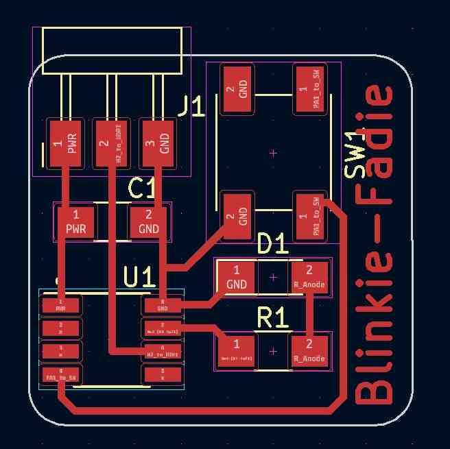
Next, I turned my attention to the PCB design. I began by opening the PCB file and clicking Update PCB with changes made to schematic. This brought in the footprints that we had linked during the schematic design. I laid these footprints out in a compact way that minimized the overlap of the nets. Then I drew a rough shape of the board outline that fit all of the components while leaving room for traces and a label. The drawing of this outline occured in two stages. First in a user layer to act as a reference and then again in the Edge.Cuts layer to make the actual edges. This two stage process made the rounding of the edges a bit easier.
Then I began to route my traces according to the nets. Luckily, my initial layout made this process relatively pain free. I only needed to cross one trace (UDPI) under another (decoupling capacitor), which was easily accomplished by running it underneath the center of the capacitor. Aside from that, everything was tracing quite cleanly. Per the advice of a teammate Barbara, I changed my minimum trace width to 0.4 mm in the board setup. To my surprise, this did not update the traces in the design to 0.4 mm. I realized that I was only changing the design rules, and not the traces themselves. I updated the traces one-by-one to 0.4, but I suspect there is an easier method to update them all at once.
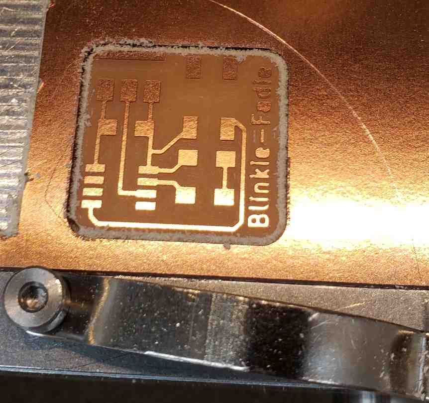
As a last touch, I added a label “Blinkie-Fadie” to the copper layer so that it would be milled.
I sanity checked my design with classmates, and Nidhie advised against one technique. Notice in the below schematic, that I traced each side of the switch together. Since the switch has two parallel channels, I would trace them together.

Basically, I had done this to make two of the stray nets disappear, to have a clean design with no nets showing. However, the internals of the switch should already have these lines soldered together, which makes these extra traces redundant. Nidhie had attempted the same technique and fried her board, with evidence of scorch marks underneath the switch. My suspicion was that the orientation of her switch was wrong, but even still I took her advice. Since there was no upside to these extra traces (aside from getting the nets to go away), but the possible downside of scorch marks, I decided to take them out. Here is my final PCB design.
Then I ran the Design Rules Checker. Most of the Errors involved stray traces and artifacts from the process of making them thicker. It gave many Warnings that “Silkscreen clipped by solder mask”, seemingly because the header component was suspended over the edge cuts. Since this was done on purpose, I determined these warnings could be ignored. Lastly, the aforementioned removal of those extra traces under the switch led to two errors of “Missing connection between items”. I attempted to make these pads unconnected, similar to how we did so for the unused pins of the 412 chip but was unsuccessful. Therefore, I decided to simply ignore these error messages and proceed.
I exported these files using the File - > Fabrication Outputs - > Gerber(s) , being sure to give it a directory and only export the layers I cared about (F.CU and Edge.Cuts). Then I hit plot.
Bantam Tools
Then it was time to mill the board. For this process, I settled on using a 1/64th bit for all milling processes and a 1/32” bit for the edge cuts. Zach, our up and coming Bantam guru, had mentioned this might lead to the best results. For settings, I used a trace depth of 0.2 mm and trace clearance of 2 mm. This led to most of the extra copper being removed from the board, as I had hoped.
Zach was right. These are the best results I have had on the bantam mills so far.
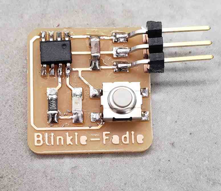
I cleaned and stuffed the boards accordingly.
KiCad - Bill of Material (BOM)
I found KiCad has a great built-in tool for generating a BOM based on the components and values created during the schematic phase. This option can be found within the schematic editor, which allows you the export as a CSV file. The full CSV file can be found with the rest of the project files in my repository here. Below are the most important contents,
| Reference | Qty | Value | Footprint |
|---|---|---|---|
| C1 | 1 | 1 μF | fab:C_1206 |
| D1 | 1 | LED | fab:LED_1206 |
| J1 | 1 | Conn_PinHeader_1x03_P2.54mm_Horizontal_SMD | Conn_PinHeader_1x03_P2.54mm_Horizontal_SMD |
| R1 | 1 | 499 Ω | fab:R_1206 |
| SW1 | 1 | BUTTON_B3SN | fab:Button_Omron_B3SN_6x6mm |
| U1 | 1 | Microcontroller_ATtiny412_SSFR | fab:Microcontroller_ATtiny412_SSFR |
Stuffing
After pulling the necessary components, I cleaned and stuffed the board accordingly.
Programming Blinkie-Fadie
This section has moved to embedded programming week, see here.
Group Project - Using test equipment
Documentation on our groups efforts to use our labs test equipment can be found here. My contribution was to work with Avery running experiments with the oscilloscope and measuring the PWM signal coming from our fading LED board.
- Circuit design is delightful.
- I designed, manufactured, soldered, and programmed a custom circuit board. I hardly knew how to do any of this just 4 weeks prior!
- Most pins on a 412 can be used for analog output.
- KiCad errors can sometimes be ignored, ASSUMING you understand what its telling you and understand the implications.
- Tinker Circuit may be a good place to start for the design of any circuit.
- Tinker Cictuit cannot yet simulate the 412 chip.
- Almost always use a decoupling capacitor between VCC and ground.
- Make sure to turn unused pins off in KiCad to avoid extra errors.
- Power lines either need to be flagged or labeled power input/output
Note: All design files and images can be accessed in my git repository found here.
All works shared on this site 'A Fab Academy Journey with Charlie Horvath' by Charles W. Horvath are licensed under Attribution-NonCommercial-ShareAlike 4.0 International![]()
![]()
![]()
![]()