
Project developement
--> Link to the group assignement page <--
Finally I have choose to make the Brian FabTinyISP who is an upgrade version of the Zaerc's FabTinyStar This board is what we call a programmer, able to program other Atmel microcontroller
Okayyy, then let's go !!
In order to build the FabTinyISP, I have to start from scratch, learn and understand the all fabrication workchain from machining the PCB to program the board with another programmer board !
Let's start with the G-code generator. It is called mods and its made by Neil ! This is a large list of modules and each modules can be associated with other modules in order to create a fully fonctional workflow. This workflow is destinate to make working (almost) every machine of Fablab !
Today our interest is focused on the milling workflow. We will use an already existing program (assembly of different modules) in order to generate the G-code who will able us to machining our PCB with an Rolland SRM-20
In order to load the SRM-20 milling program, Right click on any space > programs > open server program > Rolland > SRM-20 > PCB If all being well, you should see something like this !!
I strongly recommend that you use chrome !
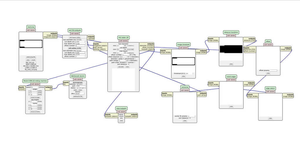
Okayy, let's start using mods !!
The first thing to do is to add a new file module who able you to save in local the resulting file !
To do this, Right click on any space > modules > open server module > file > save Then click on the output of the Rolland SRM-20 milling machine module and successively on the input of the save module. A link beetwen the two modules should appear.
Now your workflow is ready to accept your parameters.
First, select in the set PCB defaults the mill traces, in order to make a traces toolpath.
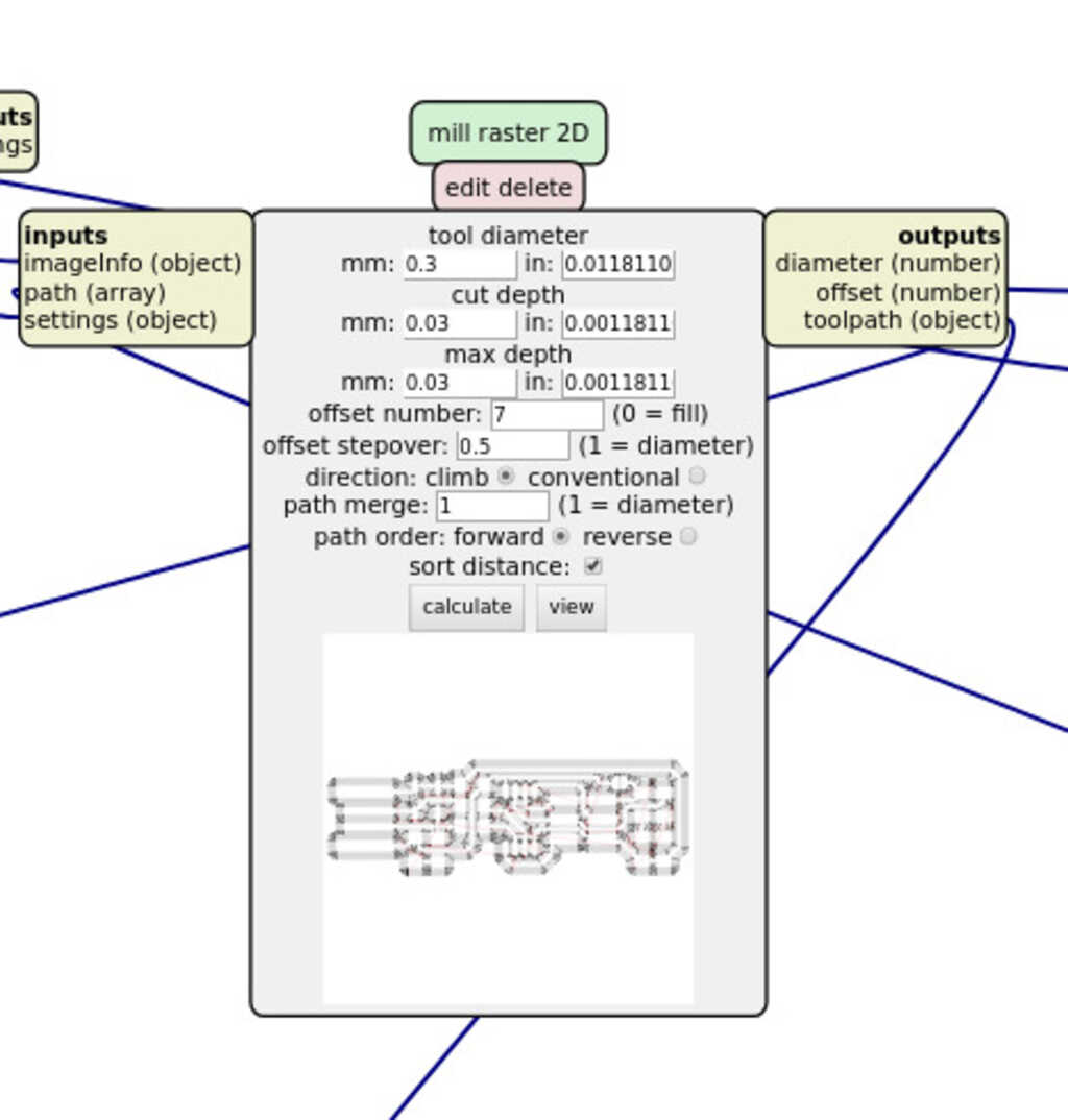
Then, in the mill raster 2D I have used this settings according to my 0.3mm conical tool.
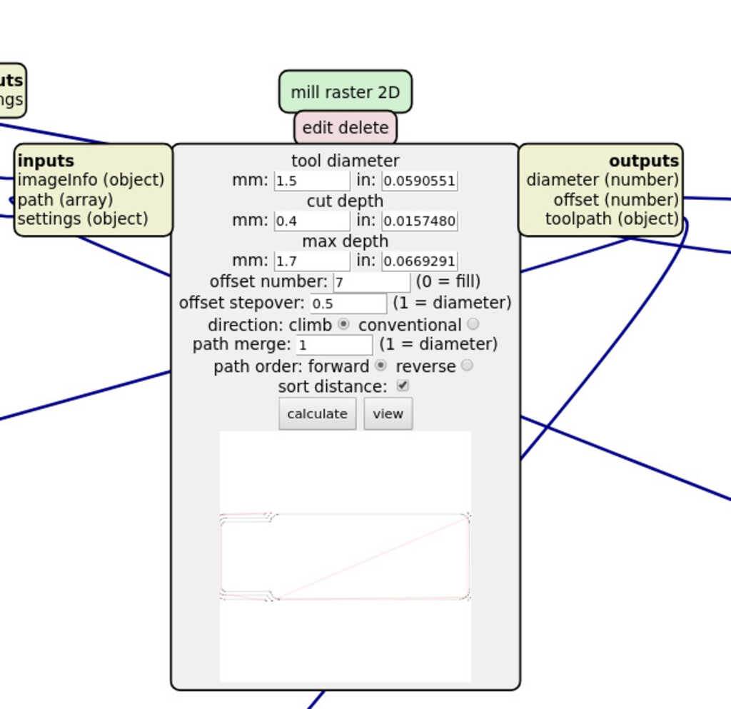
With the same method, let's start setting up the parameters for the outline toolpath.
For this toolpath I have used a right tool of 1.5mm
Edit : I have made an error in this screenshot the offset number should be 1 instead of 7. The offset means that the cutter will make the way by shifting 7 times around the trace. You will see the consequence of this error at the end of the outline toolpath.
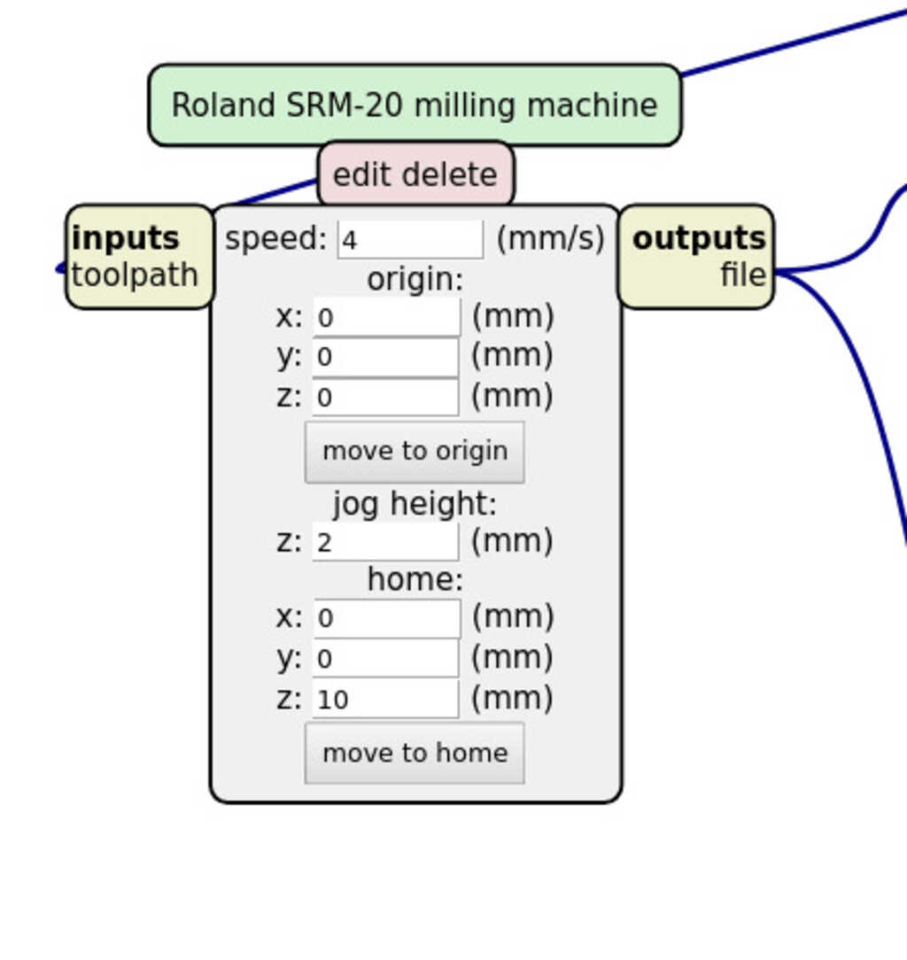
Here you just choose the origin in the SRM-20. The only thing to know is to put a Z-home superior of zero, else at the end of the machining your tool will move to the X Y home at a height of zero. And it should scratch the board... I have choose a Z-home of 10mm in order to avoid this.
Also, the jog height is the height of the tool beetwen two movement. I have choose 2mm
In order to start machining, you must have two files. One for the traces and one for the outlines. To do this, successively generate one file with the traces parameters and one files with the outlines parameters.
Click on calculate in the mill raster 2D module. If you had add the save module, file downloading should start by itself. In my case the download was not starting bacause I was using firefox. Prefer Chrome when you use mods !
Here you can clearly see in the previsualisation of the outline toolpath that path is not a simple line but there is 7 concentric toolpaths. That is useless in the cas of the outline because we just want to cut the board.
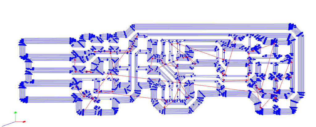
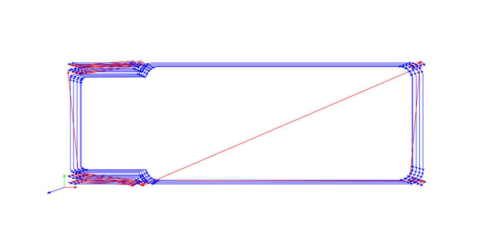
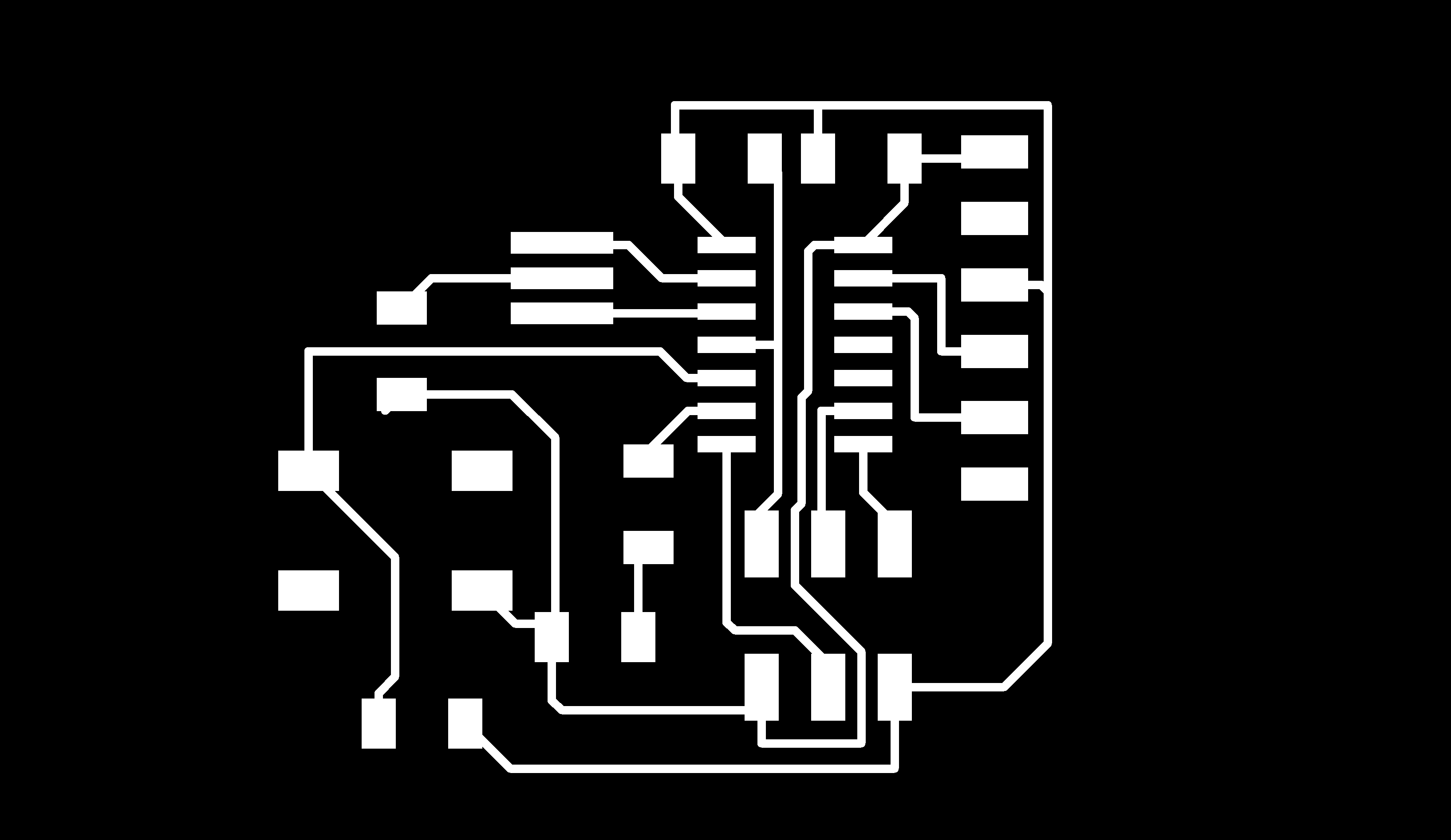
The resulting toolpaths should look like this !
Let's start using this milling machine SRM-20.
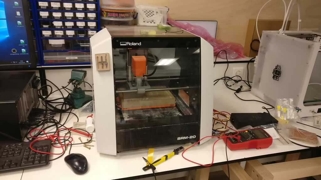
The first thing I made on it is to define the X Y Z origin.
In order to make this using the control panel of the SRM-20 I move the router to my X/Y origin and click on define X/Y origin.
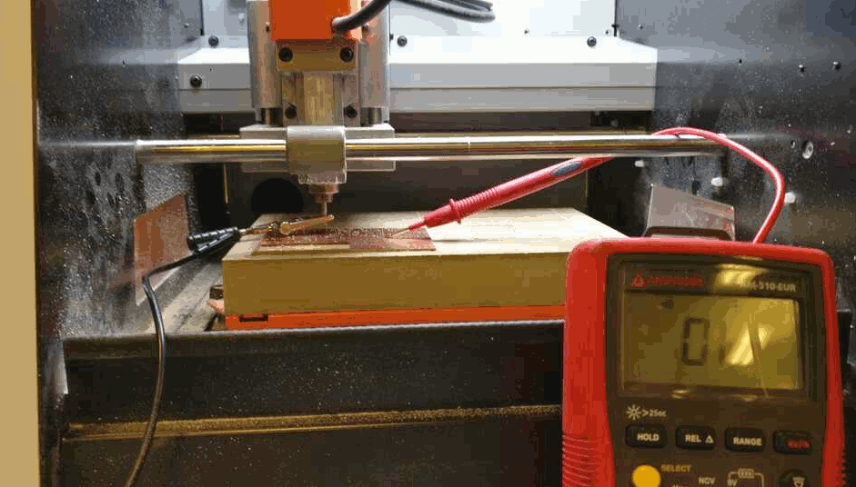
Then I have to define the Z origin. It will placed at the surface of the PCB. The SRM-20 can not make it automaticaly then using a multimeter, I put one alligator clip on the tool, and the other pole in contact with the PCB. The multimeter is set to ohmmeter, if you have on it you can set it on sound mode. It should make noise when there is a contact. I lower the tool by step of 10mm then by step of 1mm and the by step of 0.1mm. I stop it when the multi-meter make a noise. Then I just have to set this position as the zero origin.
After the traces toolpath and the outlines toolpath this is the first result. As you can see at some places of the PCB there are still some copper. I think the problem is the flatness of the PCB, it is not perfectly horizontale. Then in order to solve the problem, I have made a second pass having changed the depth from 0. 03mm to 0. 04mm. To do this, I just change the G-code using the CTRL+F fonction and remplace all of the "-3" by "-4"
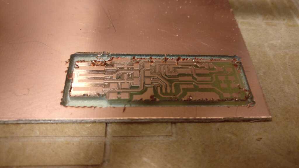
In order to avoid this kind of problem, the tips that I can give is to make the Z zero at differents place of the plate and then calcultate an average of the height and then set up the Z zero to this value. But I think that is more a question of experience. Because the way that the coper plate will be attached is very important in the final result of the milling.
This is the result afer the second pass. I can see that the width of the traces are more skinny because of the bigger depht. But this is not a big deal and I am always able to solde on them.
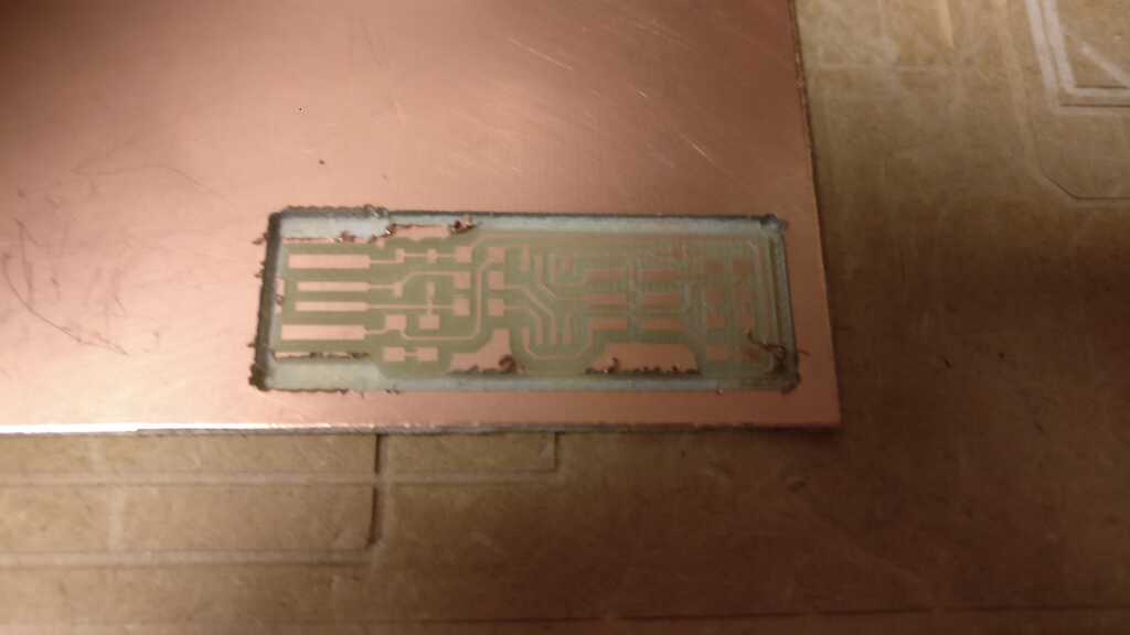
Here you can see that the outline toolpath have taked out more of the copper plate than expected because of the 7 offset that I put in mods.
Now, when your board is finished you can put it out of the rest of the copper plate. You should see around the cut a bad finish. This is normal. Just take a knife cutter and crap it in order to have a clean finish ! But be careful, do not damage the traces.
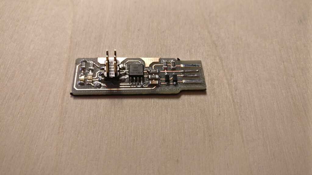
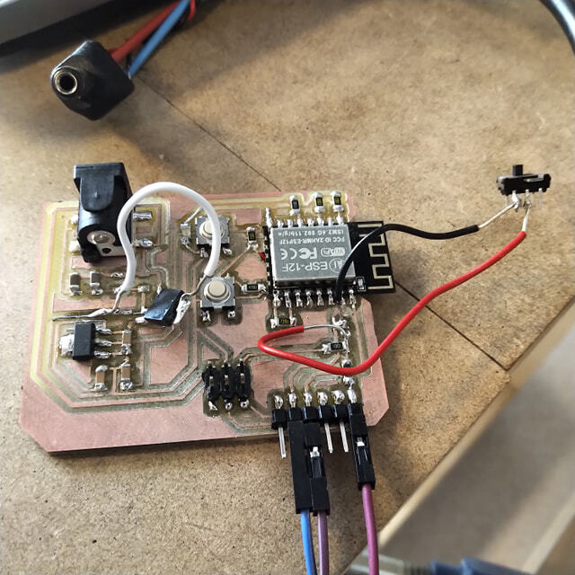
The next step is to solde all of the components on the PCB.
For this board we will use :
When you solde your component be careful of the direction of the diodes and the LEDs ! Check on internet how to interpret the direction mark of your components.
And it should look like this !
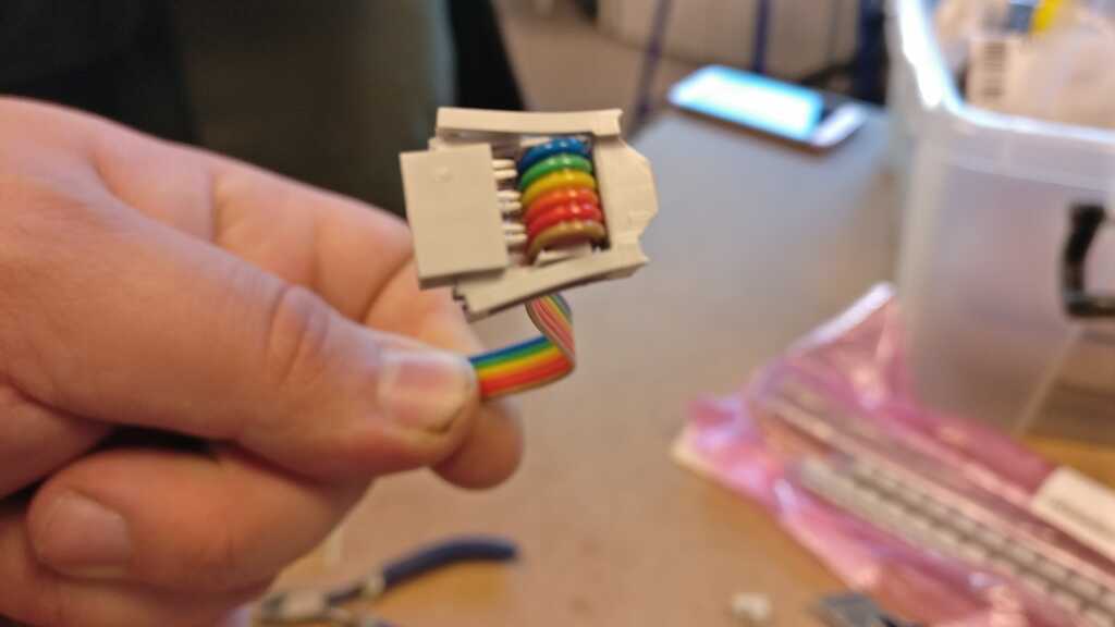
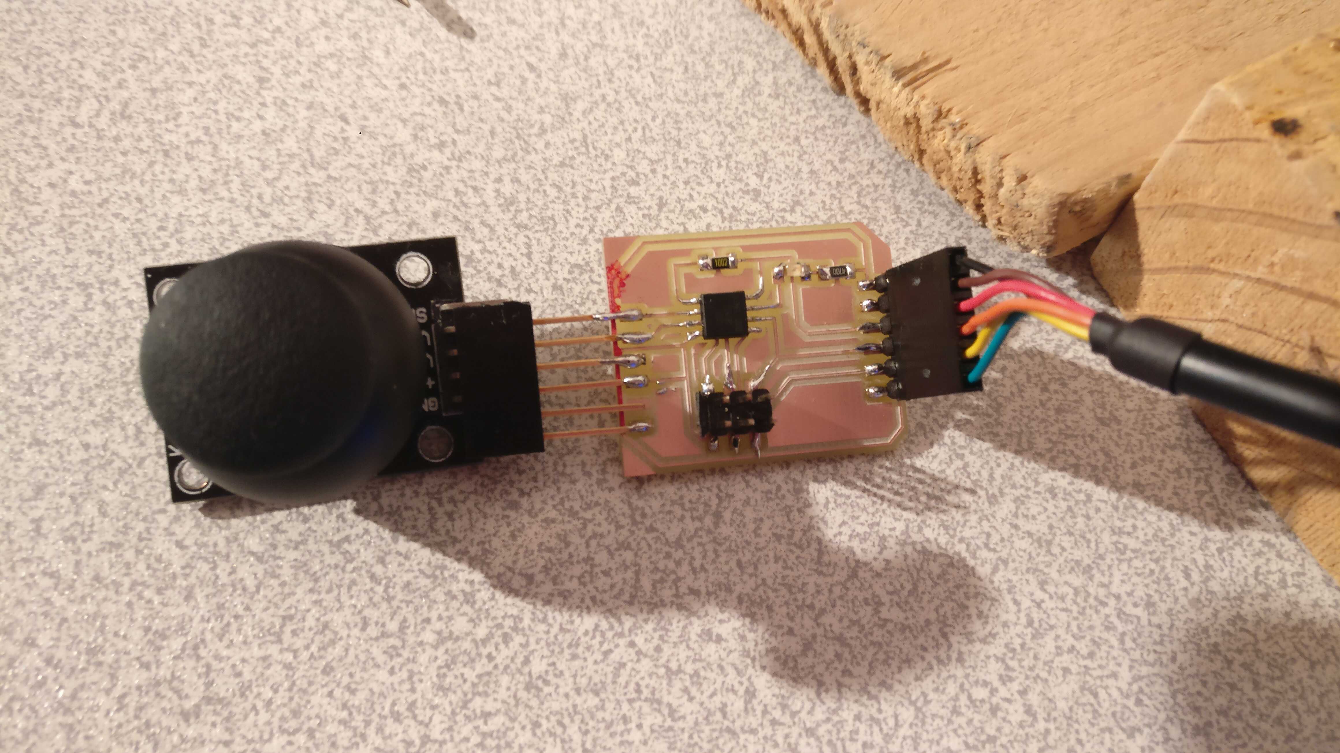
In order to test the board in the futur I have made this little six pins connector ! I didn't know the way to do it, but its pretty easy. I just have to take 6 strings of a flat cable and put it into a connector, then using a mallet I hit the connector on it top and the cable is now tighed into the connector and the contact are made.
The first thing I made for this part is to download and unzip the files for programmig the board.
All the files are on the Brian FabTinyISP page board.
I just have to unzip the files in my repo. Be careful, you have to be in the repo containing the compressed files.
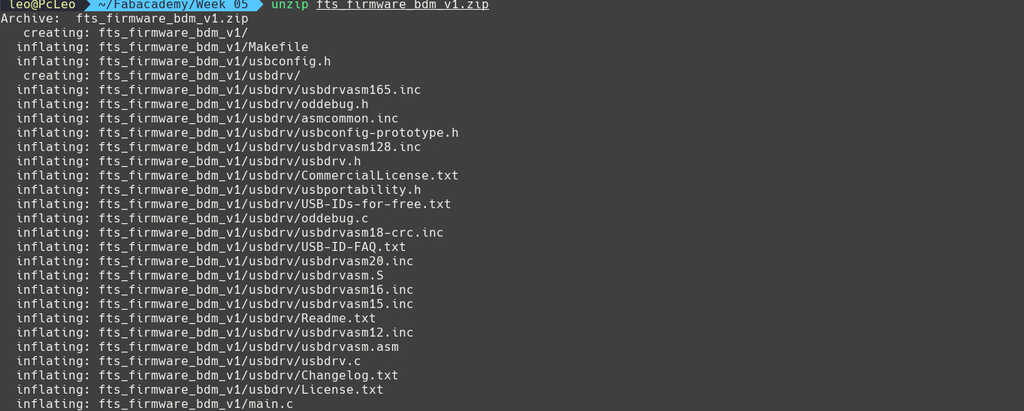
The files are now decompressed, then go into the source code repo using cd.
Before starting to programming the board you have to install all of the packages needed in order to compile and send code through an ISP pogrammer.
On archlinux use sudo pacman -S avrdude gcc-avr avr-libc make
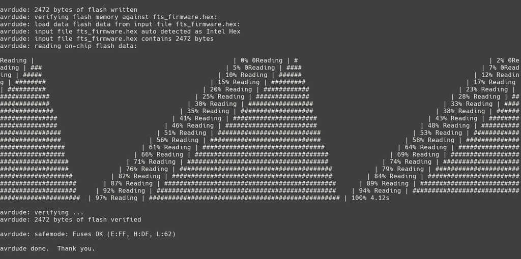
Run make . This will build the .hex file, that will get programmed onto the ATtiny45/85.
After the command finish running you should have now a fts_firmware.hex. In my case when I make this command I got a compilation warning, but don't care it's not an error !
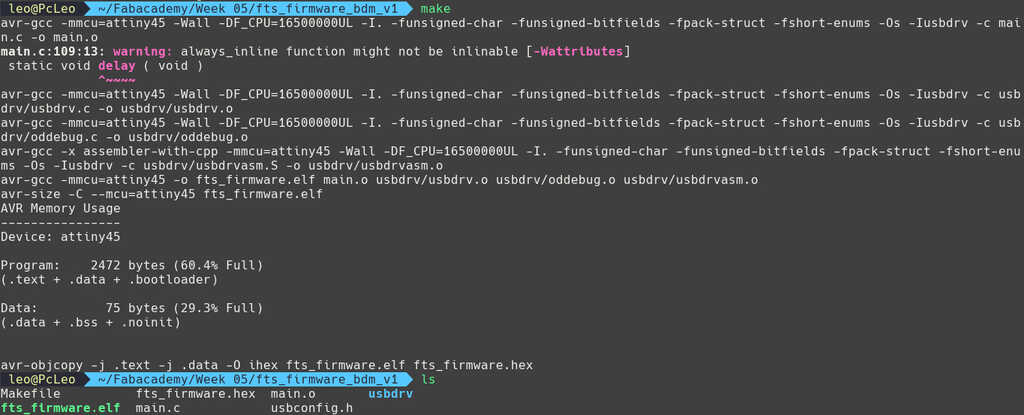
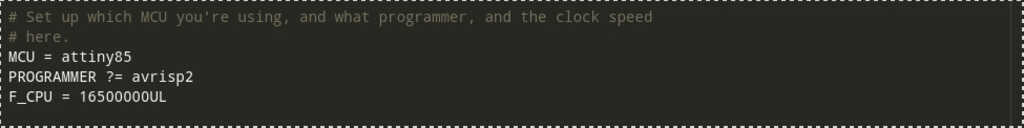
Normally, you have a Makefile into your source code repo. This file is the setup file, in wich there is all the parameters needed to set up well the board. In my case I have used a ATtiny85, and I will use this programmer Small translucent blue programmer. Then I have to specify it into the Makefile. Just change the following lines with your parameters. You can easly open the Makefile with code editor like VS-code or Sublim text.
For the following commands, I have basically follow the Brian documentation. I'm absolutely not an expert in this domain ^^.
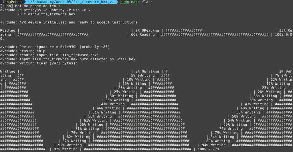
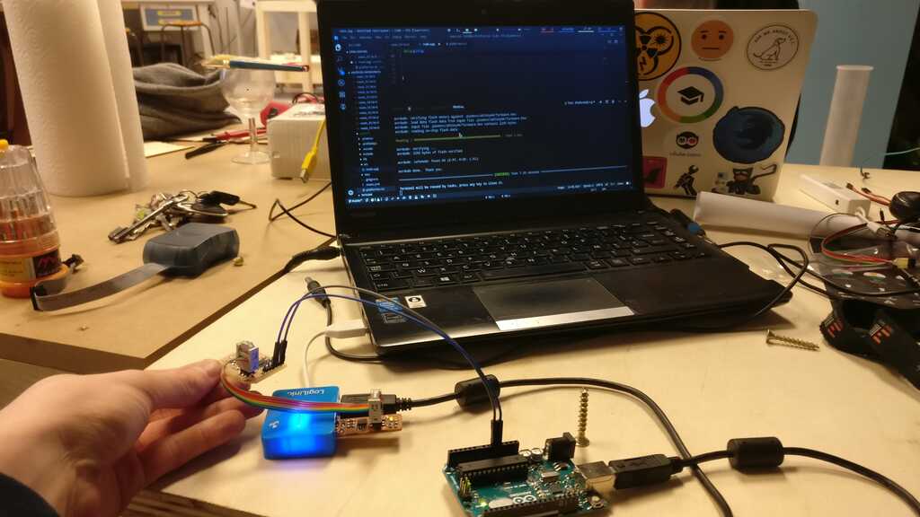
Run make flash. If I have understood correctly, this command, will program the flash memory of the ATtiny you are programming with the contents of the .hex file we built before.
At this state if something went wrong lets refer to the Brian documentation. But its probably an electronic problem. In my FabAcademy group we got some problems because of bad solder.
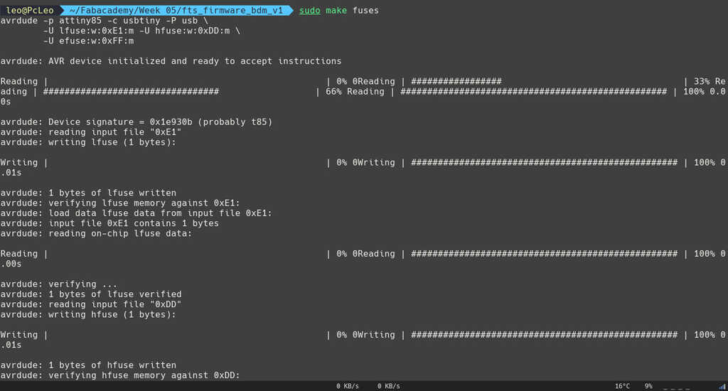
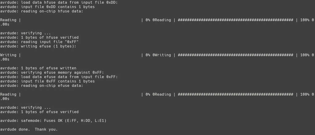
Run the make fuses command. This will set up all of the fuses except the one that disables the reset pin. Again, you should see several progress bars from avrdude. If this step fails but the previous one worked, you likely have an intermittent connection somewhere.
Okayyy, for me up to that point everything went well. But in the FabAcademy you should know that is not so easy :p
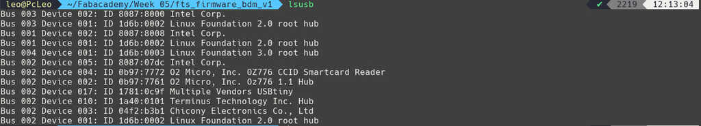
When you plug in the board into your usb port you should see your card using lsusb wich allow you to see the diffents usb peripherals. In my case impossible to see it.
In this kind of case you will need a methodic approach of how and from where the problem could come. There is two kind of debuging, top/down or down/top. The first method is to start from the software in order to test if the problem is a problem software and then gradually go to hardware test. The down/top method is the inverse, start with the hardware and go to the software.
In my case, I have choose to debug my board using the top/down approach because all of the other part of the sofware step where good and worked.
I have tried a lot things, I have started to test the board into differents comptuter and os but always the same problems. Some times using thesudo dmesg -c I was able to see that a new low speed device was plugged into my computer but this was directly follow by errors.
Then, I have tested all of my connections and solders. That was not the problem.
Then, I have tested to change my ATtiny85, for another more "safe". That was not the problem.
Making all of this changement unfortunately I broke one trace of my PCB, then I decide to make another board.
Into this another board I put some old components I had used with the last board -big error- After a new try the problem is always the same, I am not able to see the boars in my usb peripherals.
Then I decide to try to change the zener diodes, I had used them in the old board, and my intuition was that it could perhaps be the source of my problem.
New try aaaaaand thats it, I don't know why but that was my problem. If all being well you should see a Multiple Vendor USBtiny
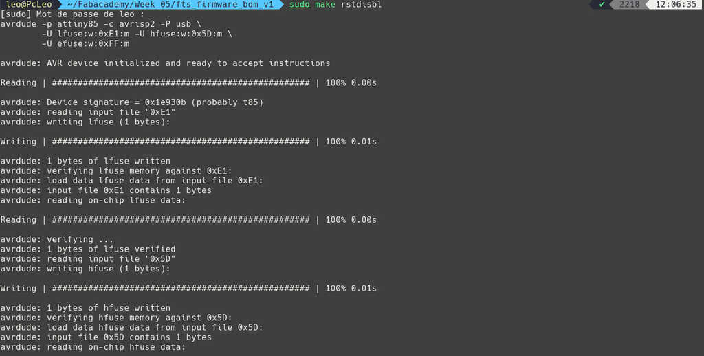
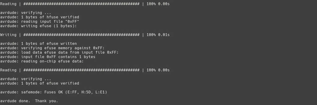
First, we need to change the bit that will turn the ATtiny45's reset pin into a GPIO pin. Once again, this will disable our ability to reprogram this ATtiny45 in the future, which is why we wanted to make sure everything was working before doing this. Connect your ISP programmer to your board one more time, and run make rstdisbl. This does the same thing as the make fuses command, but this time it's going to include that reset disable bit as well. You should see some progress bars, and with that, avrdude will never be able to talk to this chip again through the ISP header. Basically, it will disable the possibility to reprogram the board through the ISP connector.
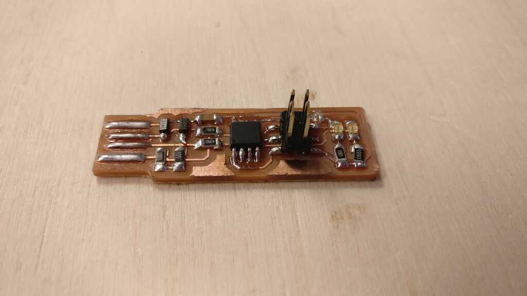
Aaannnnd you have your very own ISP programer board !! Here you can see my second board made into another type of PCB, this FR1 instad of FR4.
This week was very intesting because it open up a new world to me. A lot of possibilty are now conceivable, and the electronic field looks more funny like this rather than it was teached in my old electronic licence.
You can see this FabISP working in the documentation of the embedded programming week Link here
I guess that the more tricky part of this week was to understand how I can debbug the board... When you made your own electronic board and that you need to program it there is two levels of kinds of problems. The firts type is the hardware problem (basically the most easy to catch) the hardware problem could come from a bad solding, one component mounted upside down, a faulty component or a short circuit... (and I guess many more that I haven't meet yet). The second part is about the software, I have understand that there is some software problems because of a bad method to program the micro controller. And there is also some problems about a bad exploitation of the electronic board. The difficultie is to get quicly the good and most efficient methof to debug the problem.
fts_mini_cut.rml fts_mini_traces.rmlSee you later space cowboy
Project developement
Intelectual property
Wildcard Week
Machine design
Interface
Mechanical Design
Networking and communications

Application and Implication
Output device
Input device
Molding and casting
Embedded programming
Computer-Controlled Machining
Electronics design
3D scanning and printing
Electronic production
Computer controlled cutting
Computer-aided design

Versioning and Website
Idea of my final project
How to modelise a longboard
For any suggestion, help or featured project