
Project developement
--> Link to the group assignement page <--
On my Linux I first started to think about using KiCAD, but after a little research I have found an ArchLinux version of Eagle and decided to use it.
Eagle work with two types of workspace. The first one is the schematic view, it able you to connect theorically all off your components, once the components are connected you must switch to the board view in order to design the real shape of the board.
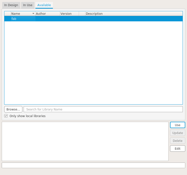
The first step for me is to install the fab.lbr library . This library made by member of the FabFundation, contains most of the components we need and we have in a fablab. This library is very important for the Fabacademy and the all of the fab community because it allow to have to use in homemade fabrication most used componenents for basical electronics. Without this library you will need to create your own or download another from internet.
Ok now I have all of the components I need !
The first step is to put into my workspace all of the components I will use. I started by reproduce the Hello board and after I will add the button and the led
I have used the add part menu and all the components i need are in the fab library ! At this step we don't have to take care about the placement of our components
List of the components :
Be careful when you select your components, they are mostly defined by there sizes. In a fablab most of them are 1206 size.
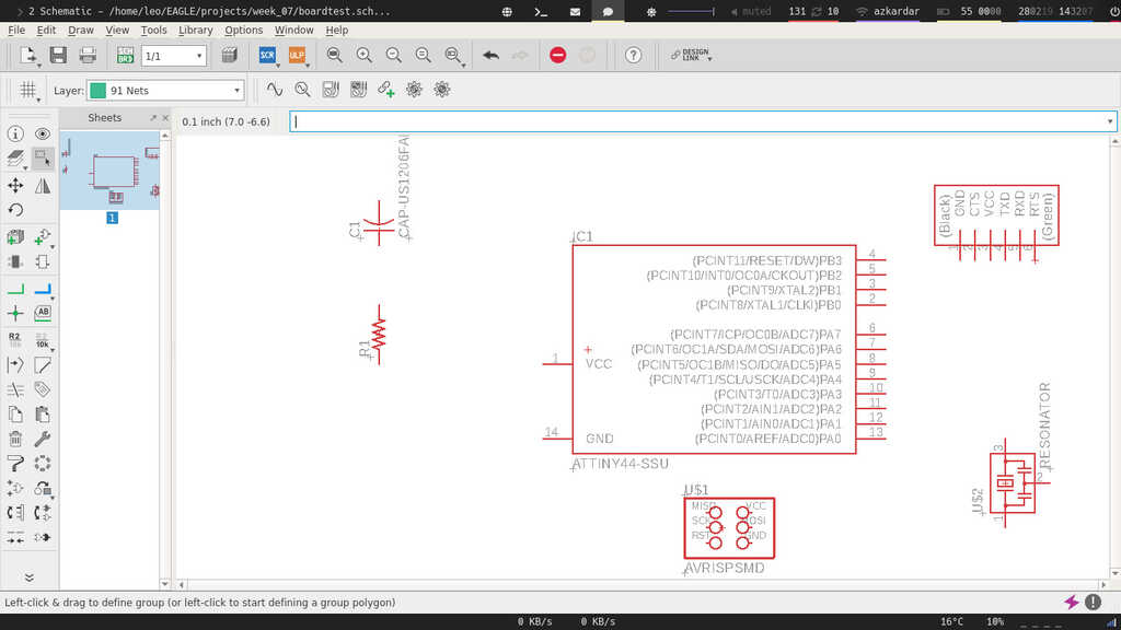
Now let's connect all of them together in order to have a fonctionnaly board !
To do this I have used the schematic view of Neil, and with the NET tool I have created some "string" connected to every pin i will use.
After this, rather than connected them chaotically. I have used the name fonction. By naming all of the pin you want to be interconnected with same name Eagle will automatically connect them virtually.
The result should be something like this :
Ok, at this state my schematic view is exactly the hello board !
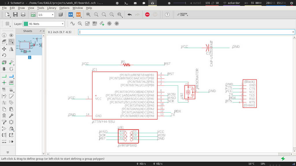
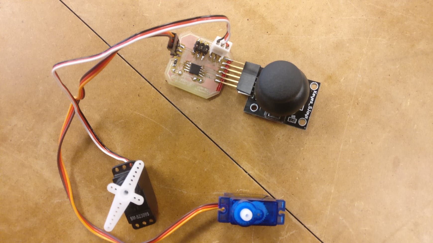
Let's add the led and the button into this schema.
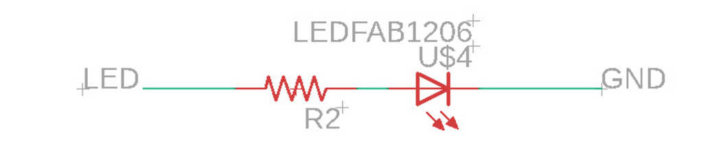
Basically the led must be connected through a resistor to a pin of our microcontroller. Here I have decided to name the pin A7 of my ATTINY into "LED".
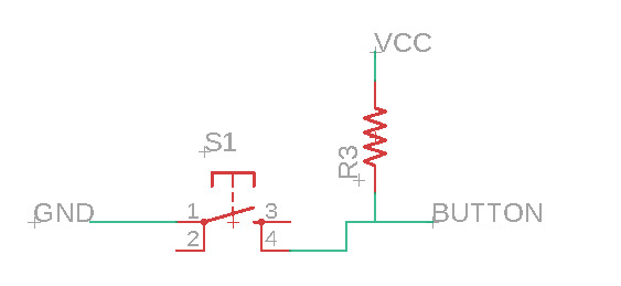
Connect a led to a microcontroller is pretty simple but connect a button to a micro controller in order to read a value (open or close) is not so trite. In order to understand how it's work we found a really good documentation.
Basically, it explain that you have to connect the alimentation (VCC) to a pin of your board and when the button is pushed the electrical current go to the ground. But be careful to put a resistor beetwen the VCC and your button else when the button will be closed it will create a short-circuit. I have made this error in a first time and then I modified my schematic.
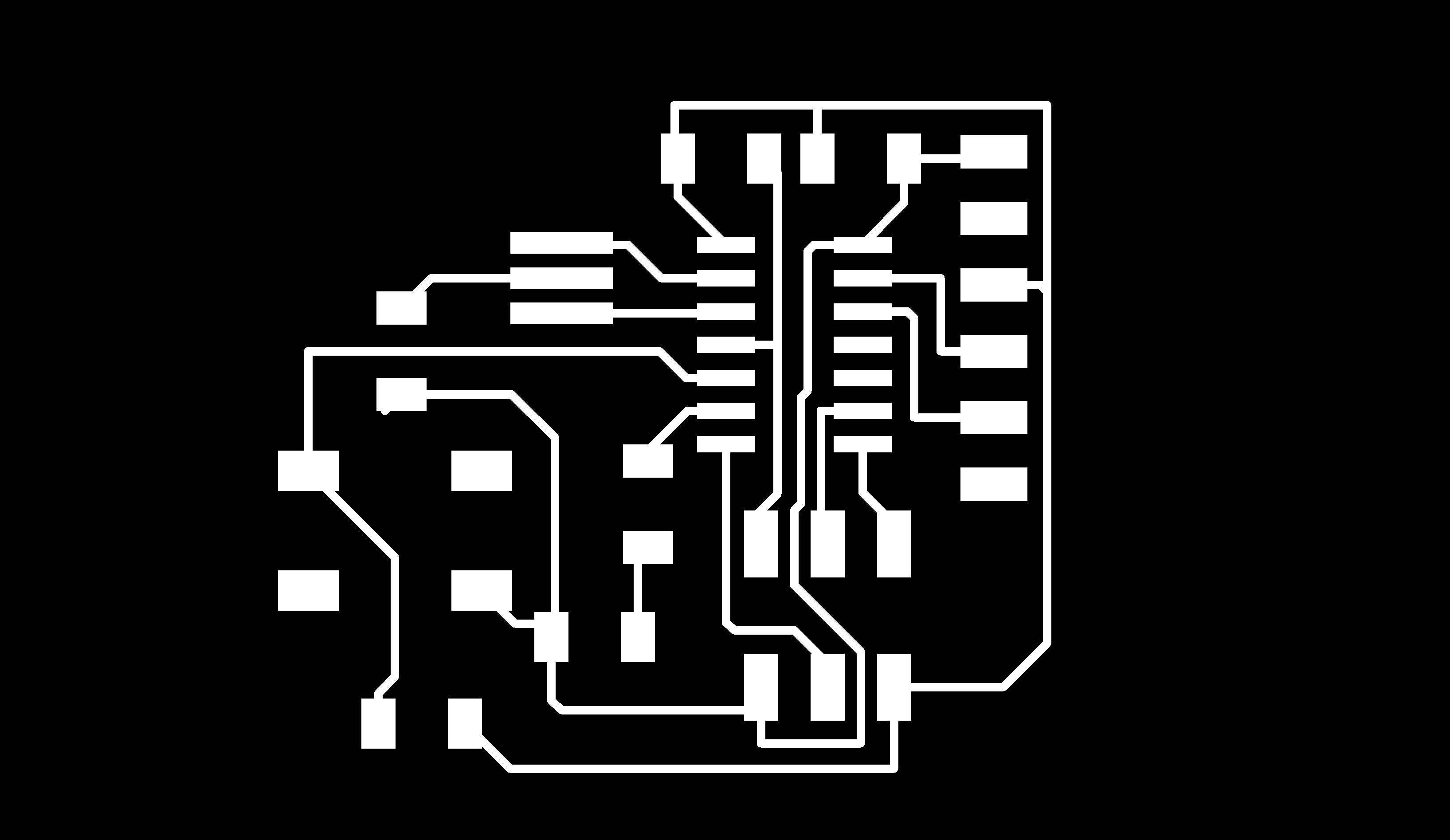
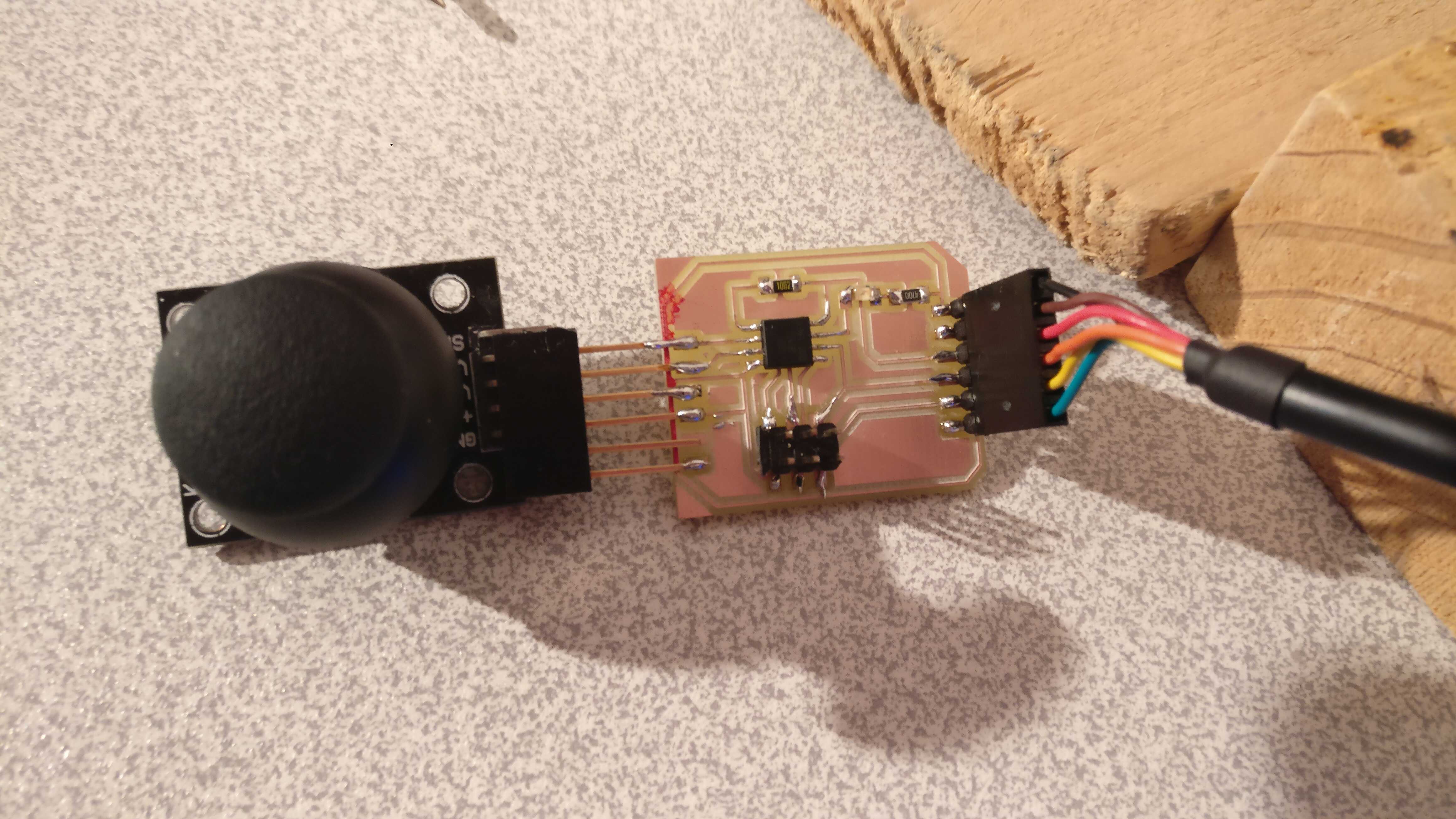
Now let's design the "real" board. First when you switch to the board view all of your components will places in bottom-left corner with a lot of yellow strings beetwen them.
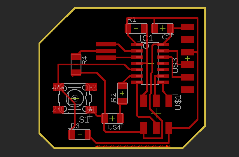
In order to place them I have reproduce the same board of Neil. One tips is to put the ISP connector at the bottom of the ATTINY44. After, crudely placed the components lets make the traces. Use the route and set the thickness to 12. Default it must be 6 but this is to tiny and the result will be bad.
Now I have added the button and the led.
Little tips, when you can't find a way to connect two components you can use a 0Ω resisor in order to go over an existing trace. Here the R4 is a 0Ω resistor.
Now I will talk about the different eagle tool that are used in order to check your boards.
Basically the ERC is the "Electrical Rule Check". This is a handy little tool that you’ll always want to keep in your engineering toolbox, as it helps to point out common errors in your schematic. An ERC will check for the following issues:
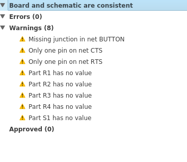 As you can see I have no errors displayed in the panel, only some warnings. This mean that it could be a problem but this is not critical. It depends of the user and he want do with his board.
In my case :
As you can see I have no errors displayed in the panel, only some warnings. This mean that it could be a problem but this is not critical. It depends of the user and he want do with his board.
In my case :
Now let's see what is the DRC :
Basically, the DRC "Design Rules Check" are a lost of options and settings that allow you to set up the design rules of your PCB.
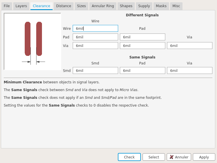
This very useful in order to avoid some problems during your machining. But also it can be used in case of complex PCB with more that one layer ! With goods DRC you will be able to use the auto-route function. Most of the time this function is useless because the resulting routing is often really bad and not optimised. In order to design the yellow outline go to the milling layer or dimension layer and use the wire function. Just draw the outline of the board and it's all good.
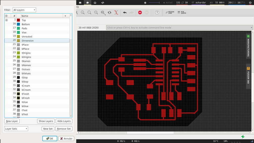
Okayyyy, now the design of the board is complete. The next step is to export it. When we export it we have yo differentiate the traces and the outlines. We also to undisplay the pad name and other informations. To do this :
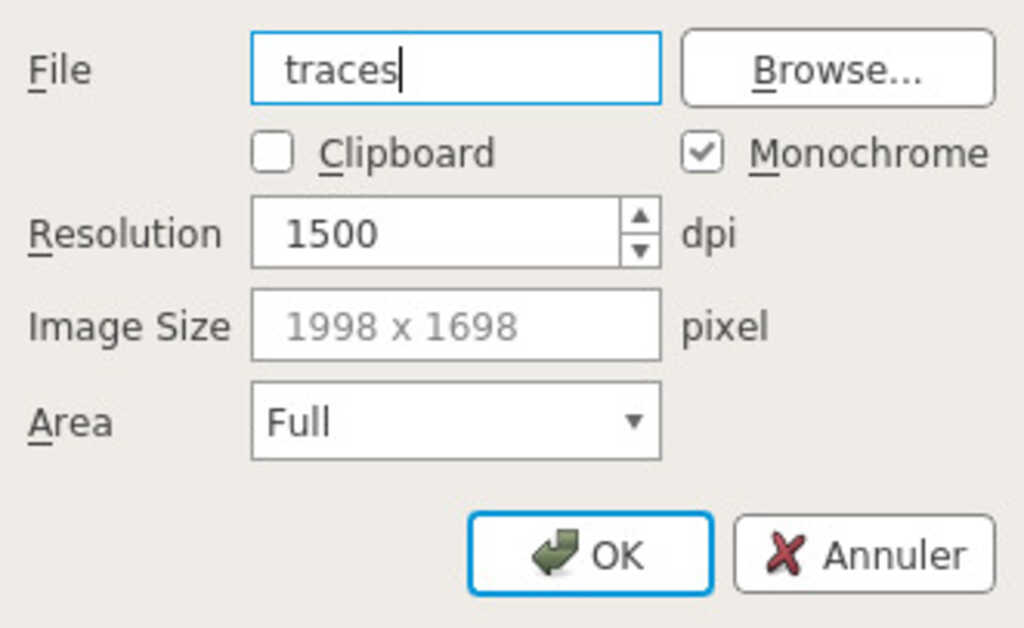
The result must be something like this :

In order to export the outline, I have followed the same method by selecting the milling layer :


The machining is exactly the same method and parameters of the Electronic production week.
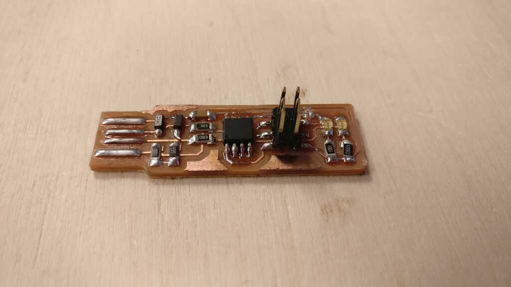
The board with all the components :
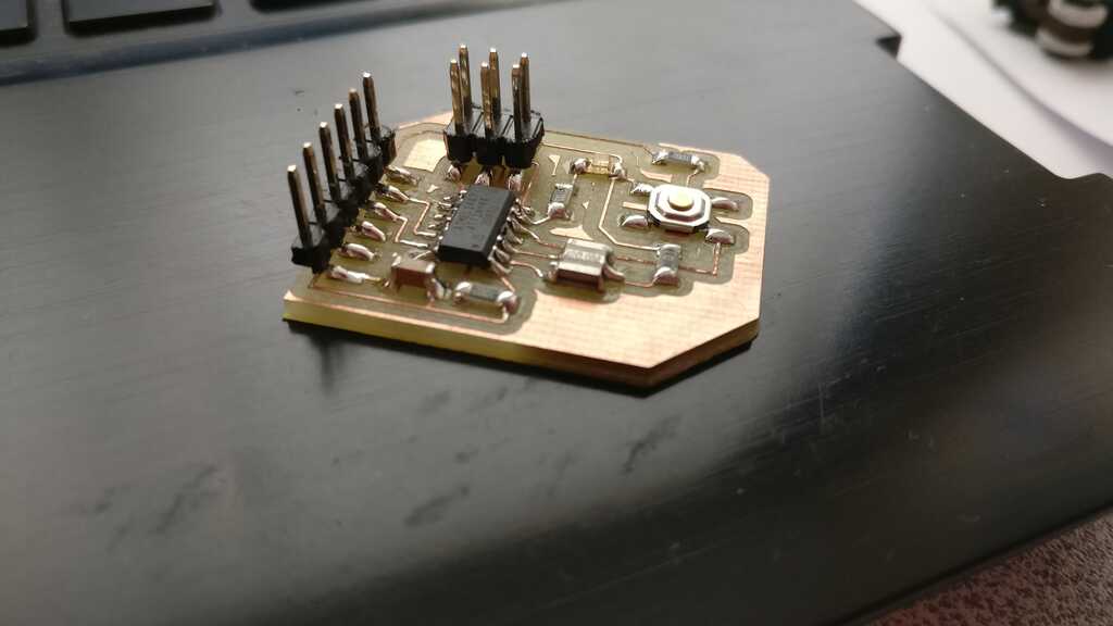
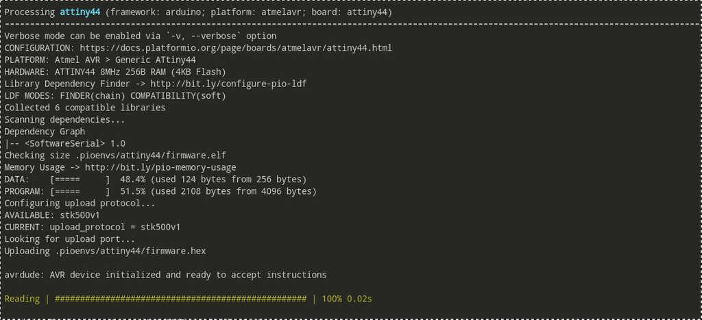
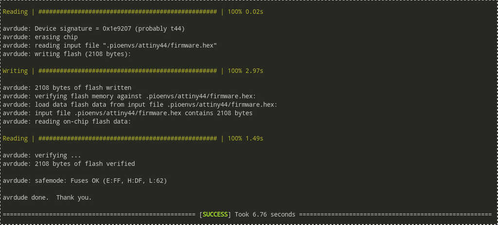
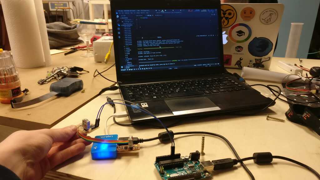
And after a lot of troubles caused by a short-circuit because of a bad placement of my resistor in the button part. I'm able to program it !!
Project developement
Intelectual property
Wildcard Week
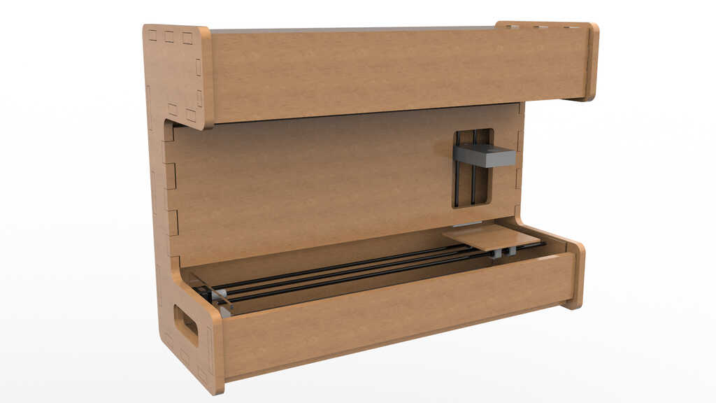
Machine design
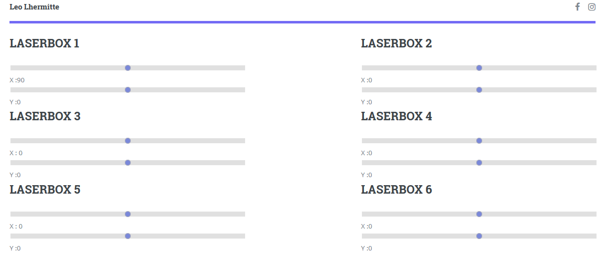
Interface
Mechanical Design
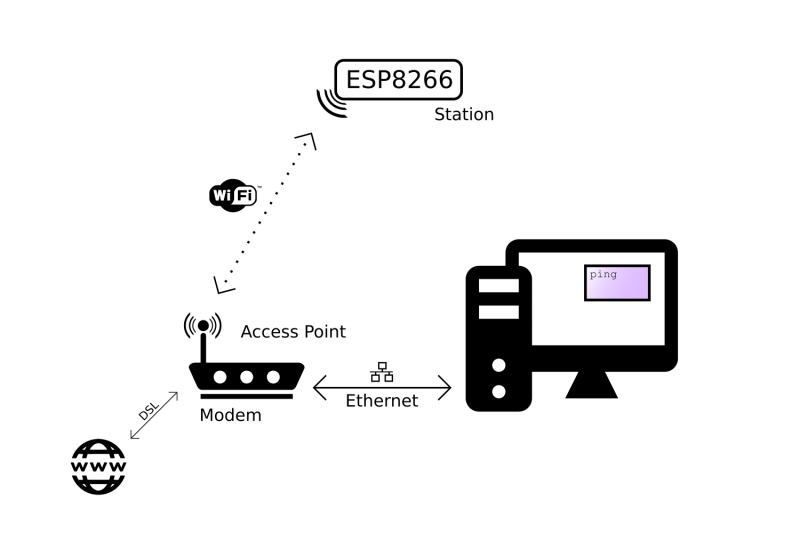
Networking and communications

Application and Implication
Output device
Input device
Molding and casting
Embedded programming

Computer-Controlled Machining

Electronics design
3D scanning and printing
Electronic production
Computer controlled cutting
Computer-aided design

Versioning and Website
Idea of my final project
How to modelise a longboard
For any suggestion, help or featured project