Week 7. Electronics design
The main objectives were to design, mill, solder and test a printed circuit board and Observing the operation of a microcontroller circuit board as group work.
Designing with the Eagle
Schematic design
After installing the Eagle software from Autodesk the component library needed was downloaded and added to the software.
To begin with, download the component library file.
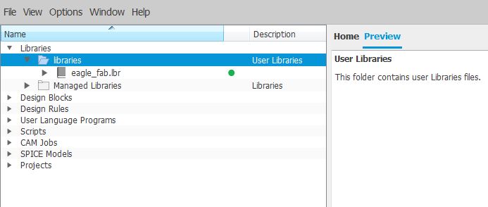
Then save the fab.lbr file in the default path of libraries of the eagle. Eg. (c:\\My Documents\EAGLE\libraries).
When eagle software opened and go to the library menu, the new fab library should be visible under user libraries.
After referring to the lecture and the board layout provided by the fab academy I started with the schematic design.
To add a new component after creating a new schematic, press add part button>browse the library>select the component needed
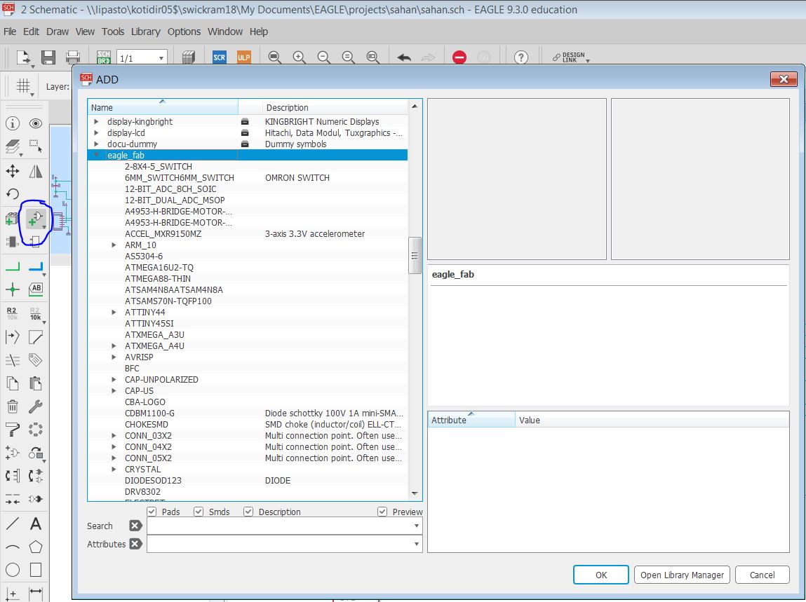
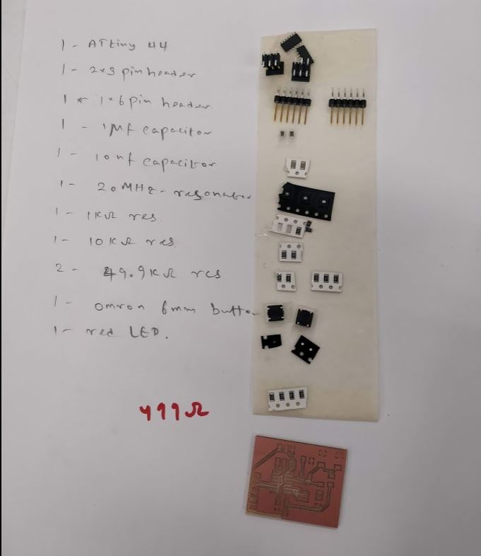
To complete the design these components were needed.
- ATTiny44-ssu (fab> ATTINY44)
- Resonator (fab)
- AVRISP SMD (fab>AVRISP)
- FTDI SMD Header (fab)
- C-EUC3216 (C-EU)
- Omron switch B3SN-3112P (fab)
- LED FAB1206 (fab)
- RES-US 1206FAB (fab>)
- Vcc (supply1)
- GND (supply1)
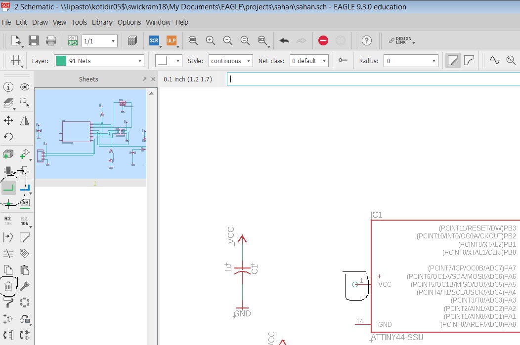
After placing the components roughly, to move components, select Move tool and click the cross on the component needed to be moved, and drag it. Then to connect components use the Net tool. Make sure to start creating a connection when the green circle can be seen on the pin of the component. The delete tool can be used to delete a net already made. While designing the schematic,Anti's design was referenced.
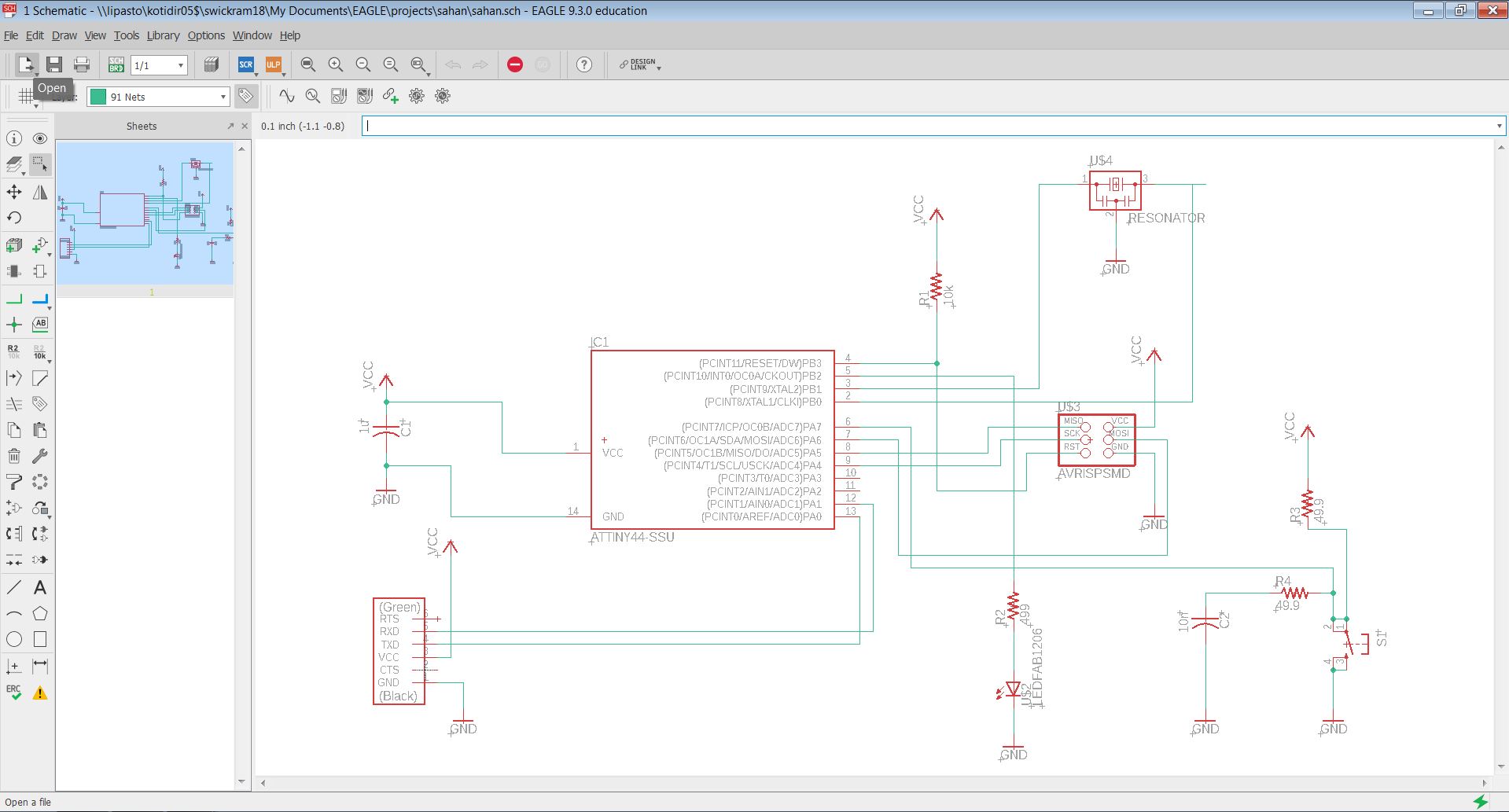
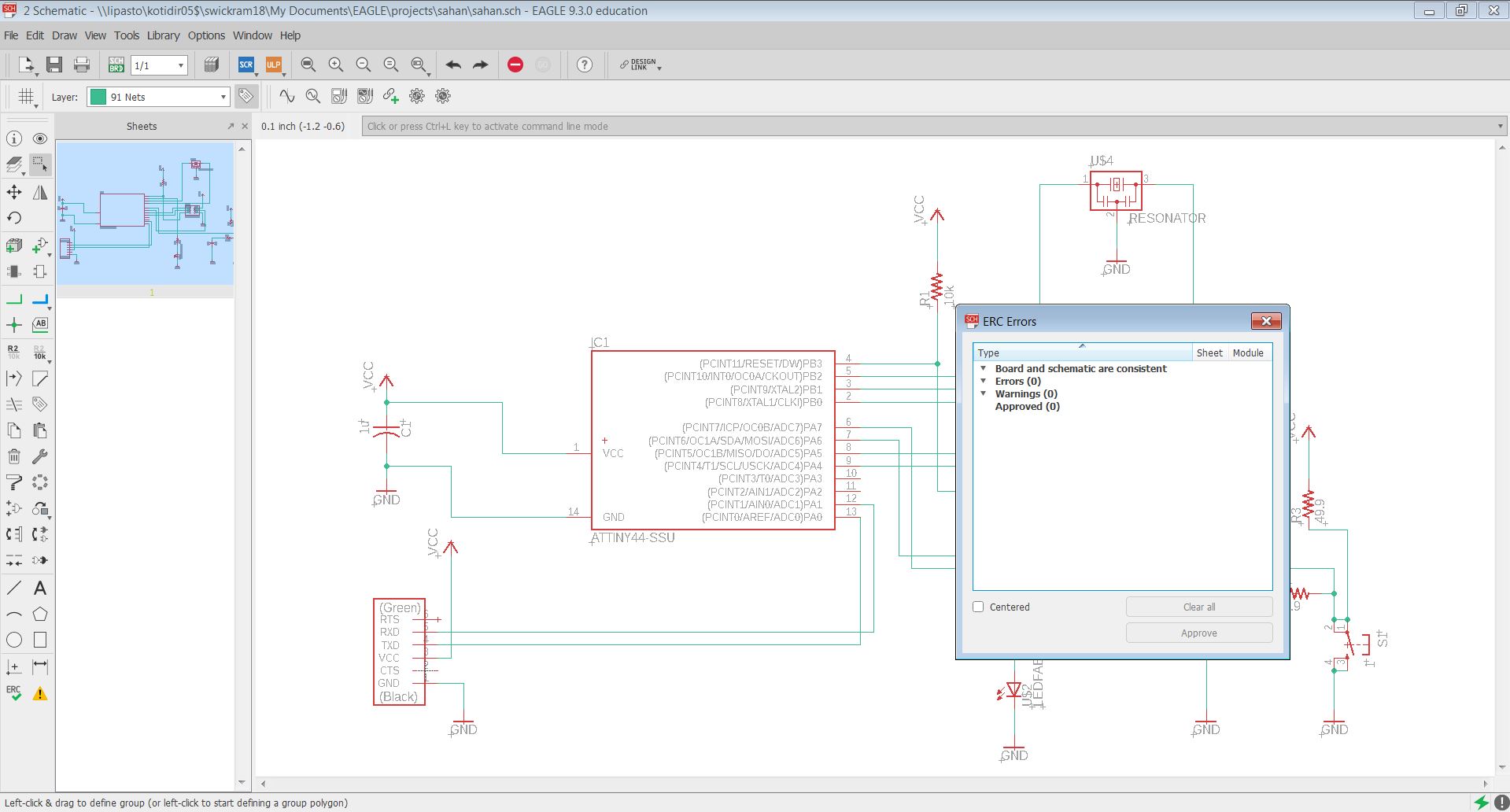
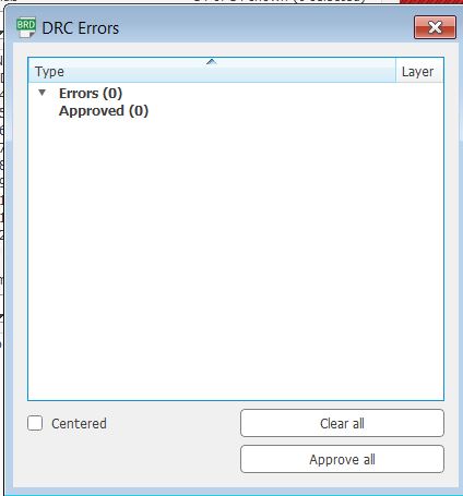
Final schematic design can be checked for errors using ERC. If there are no errors then it will be visible like following.
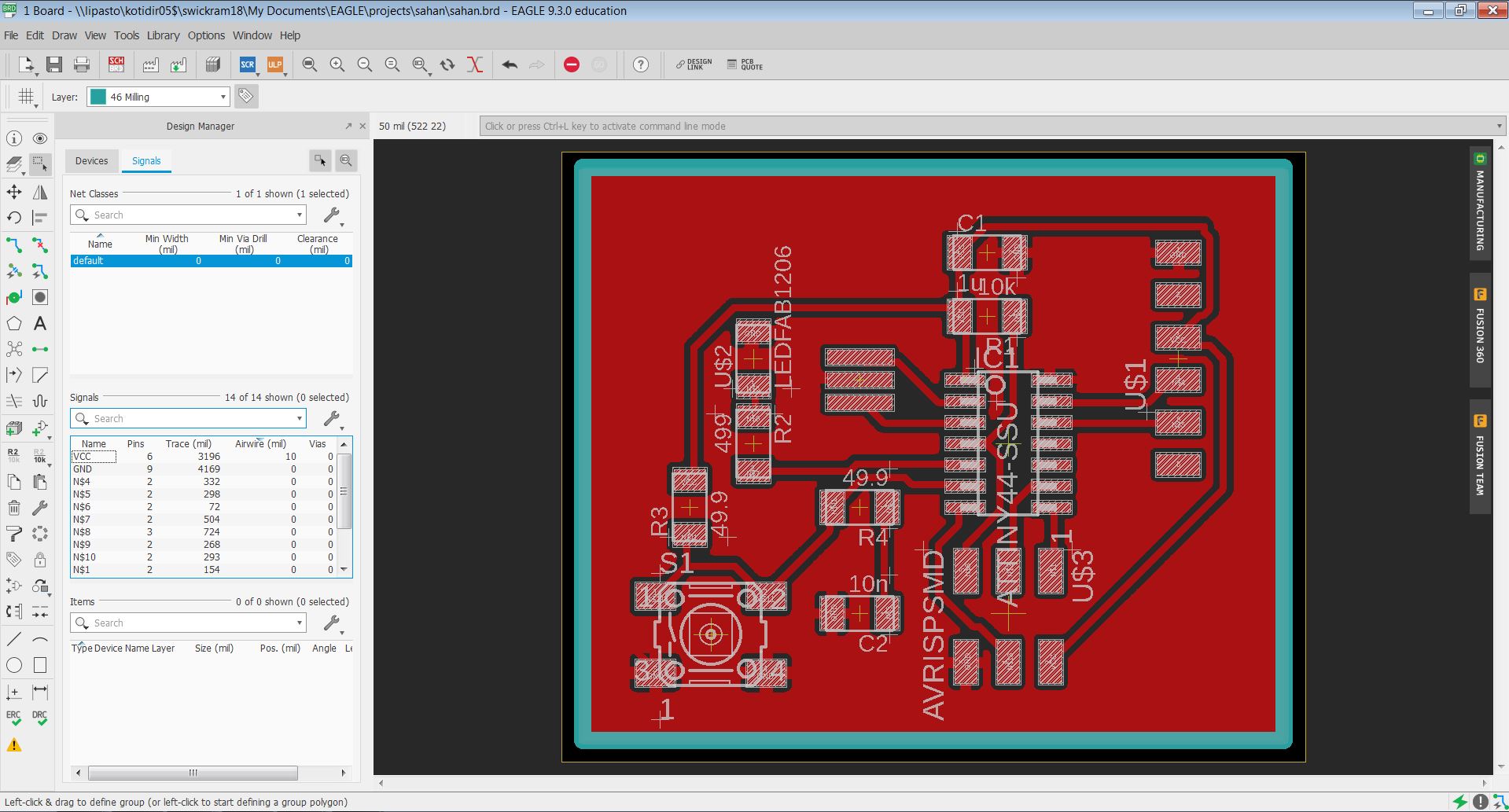
Layout design
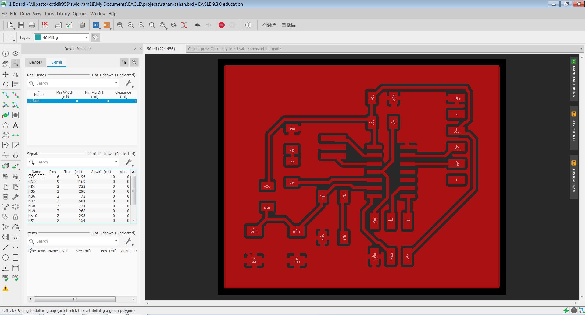
Once the schematic is completed, the traces need to be made. Initially, press Generate/switch to board button to generate layout. It will be a representation of the layout components and how they should be interconnected according to the schematic connections.
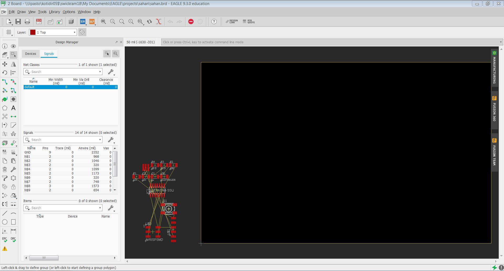
After placing the components roughly the routes has to be created such that they cannot overlap.
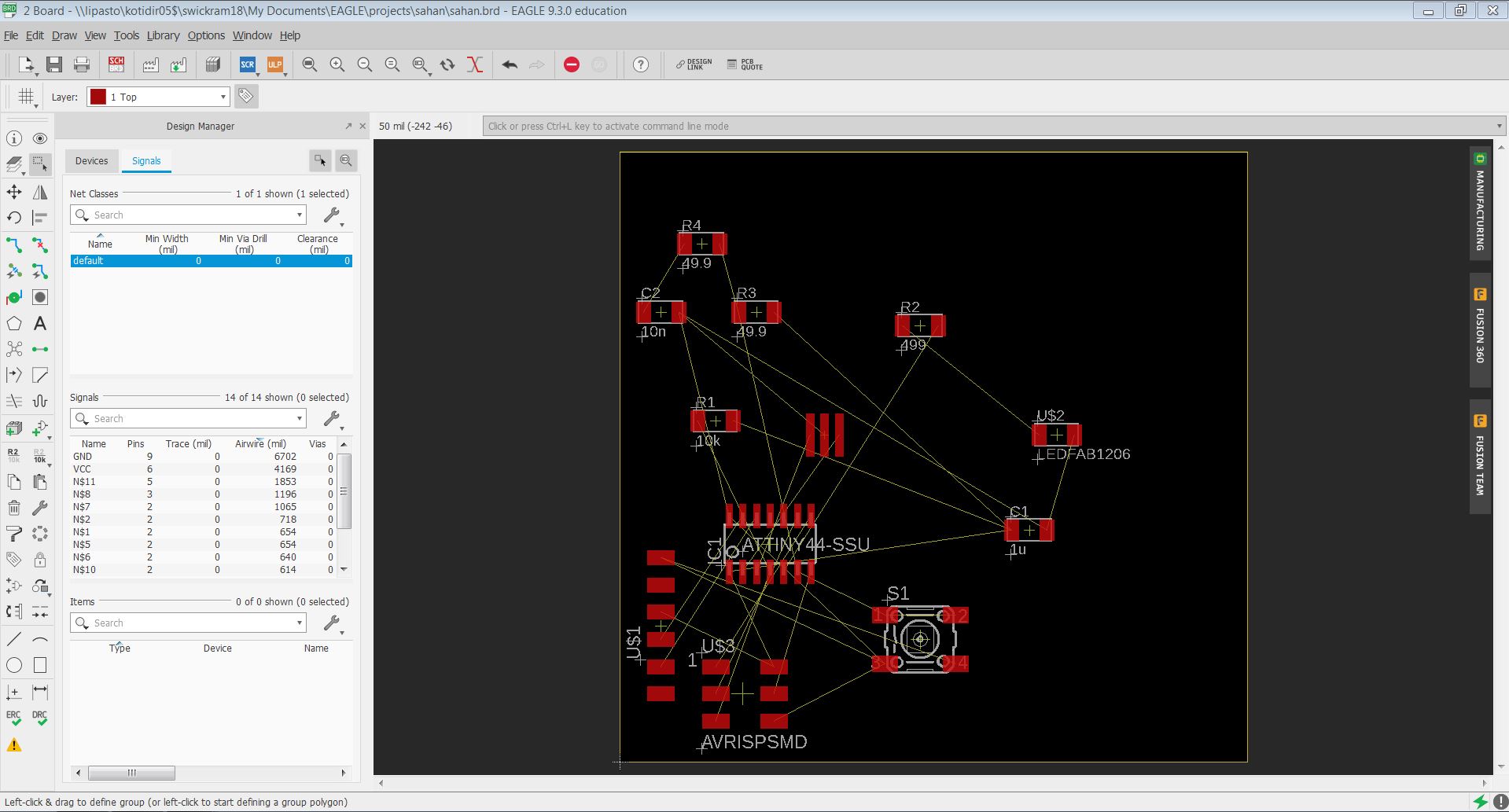
These tools were useful when placing the components as required.
Edit > move and Edit > rotate to position
Edit > Route to create routes from one component to another
Edit > ripout to delete a route
Tools > ratsnest to reorganize airwires
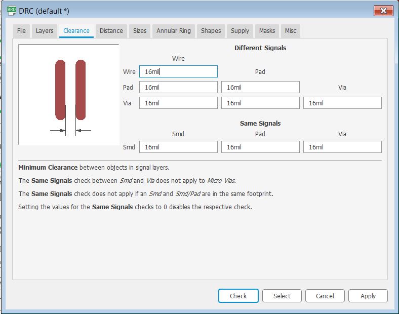
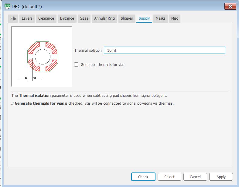
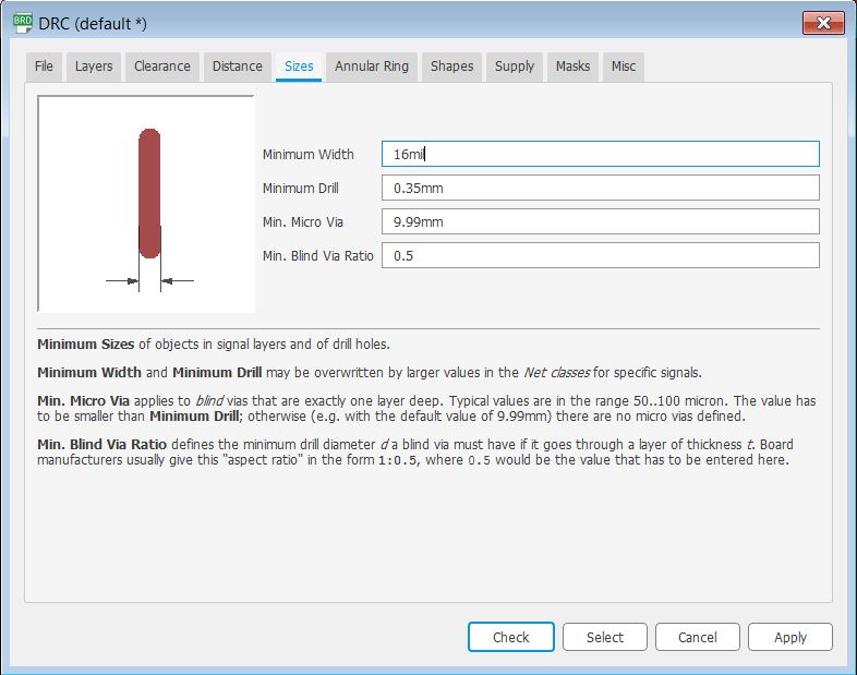
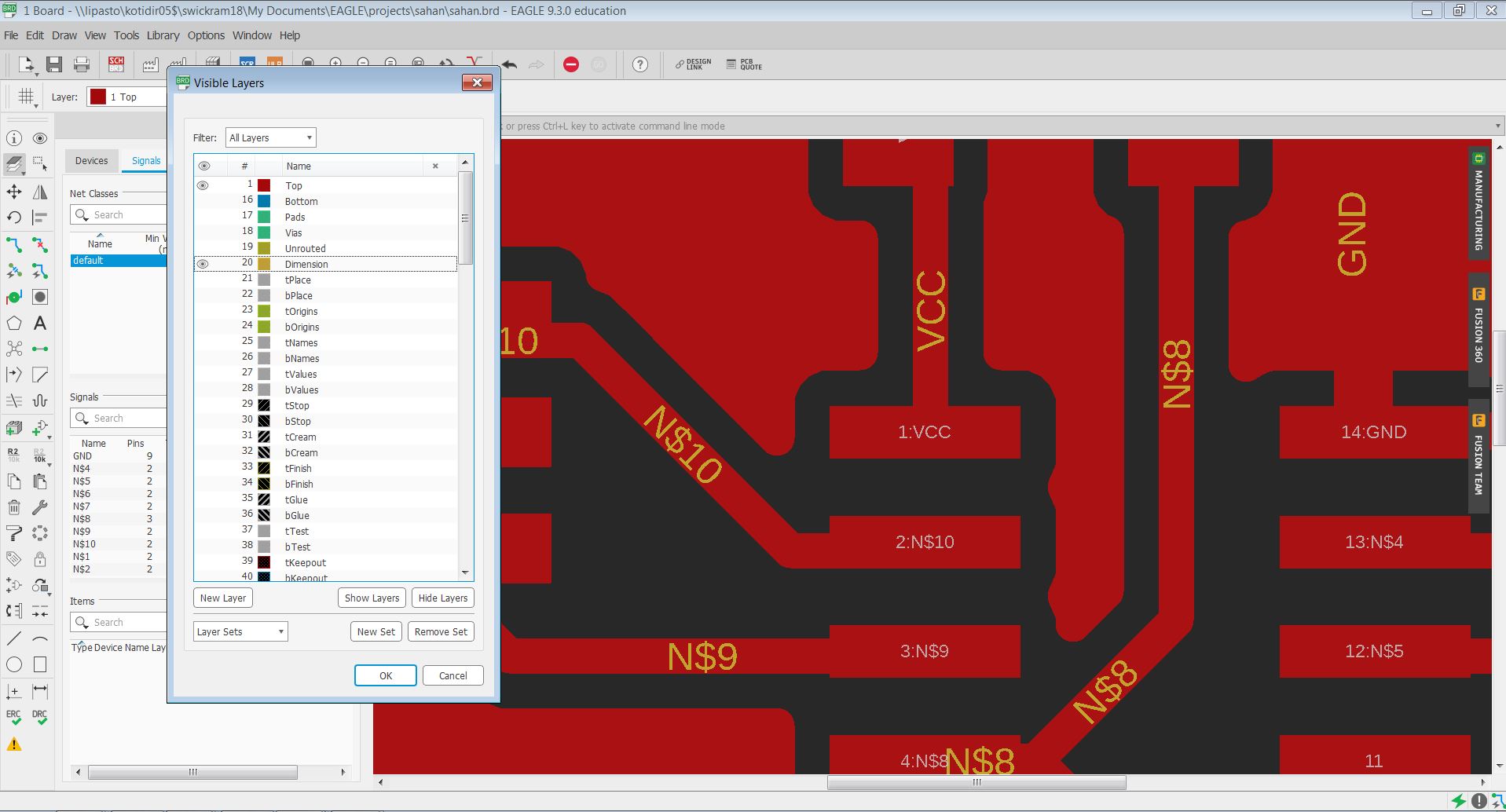
In the design rule check (DRC) these parameters have to be changed because the mill bit size is to be used is 0.4mm.
After making the traces the ground layer has to be made.
To define the ground layer as the remaining copper in the board:
Draw > polygon: Draw a polygon around your board
Edit > Name: Name it GND
Tools > ratsnest: To connect wires to the ground layer
Finally, the DRC errors have to be checked.
Next outline has to be made. The outline for cutting was drawn in layer 46 (milling) with Draw > Line, setting the width to 40mils which is almost equal to 1mm bit used for milling.
To export the png file these steps have to be followed.
File > Export > Image- for the outline, select only Milling layer(layer 46)
- for the traces, select only top layer.
- select monochrome
- set resolution to atleast 2000dpi.
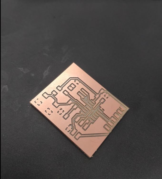
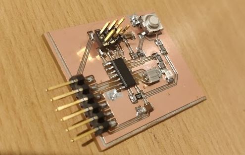
Milling and Soldering
Here the same process described in Week5 to manufacture the board was followed. In Fab Mods the cut depth was set to 0.36mm and made the rml file for SRM-20 milling machine.
Next, I soldered the components used in the schematic design.
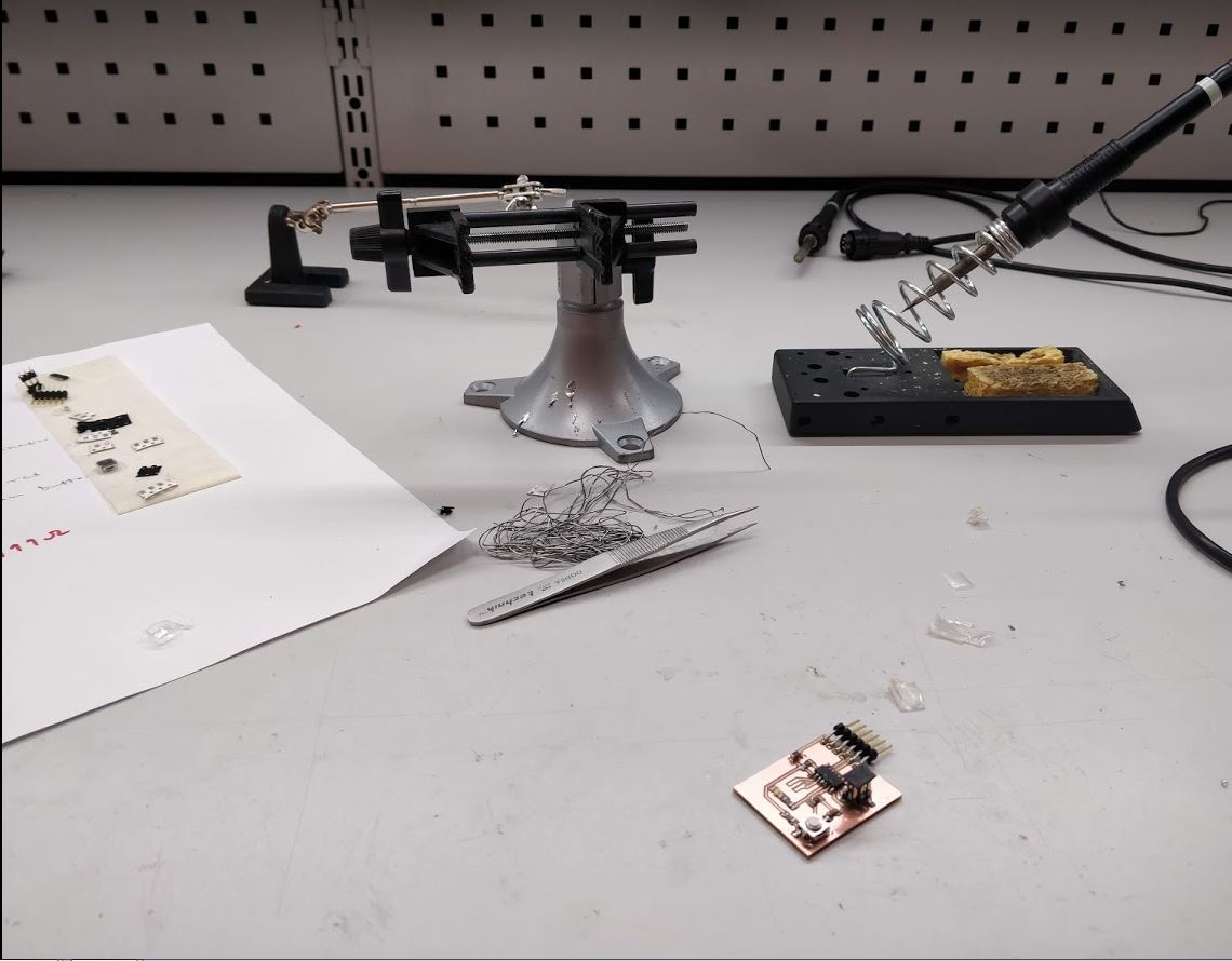
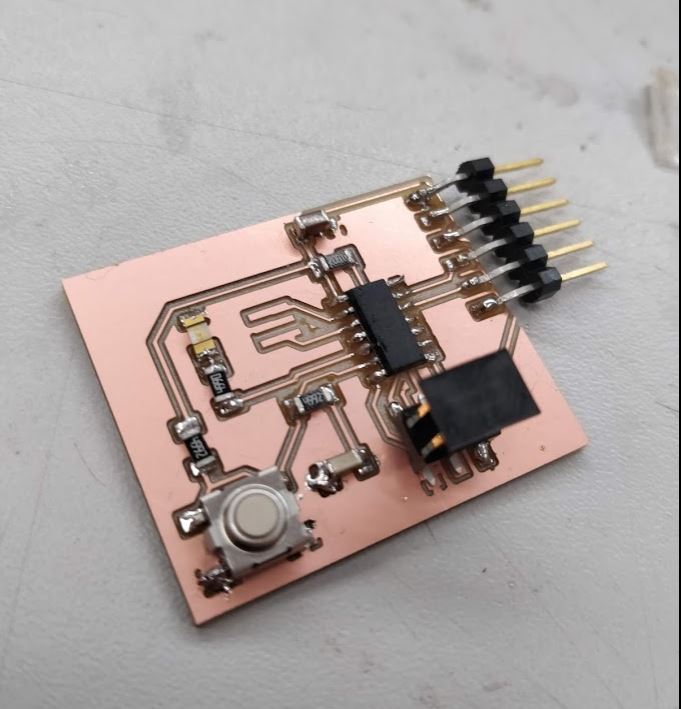
However, it was observed later that milling from the machine has removed one trace needed therefore the board was milled again using different outline file. But for the milling I have used the v bit and I changed the Z height to 6um after failling to make propoer lines. Moreover, there's a deep milled groove visible under the connector in the new board because my new outline file was much larger than the board. Although it did not matter while soldering the components.
Progamming and Programming
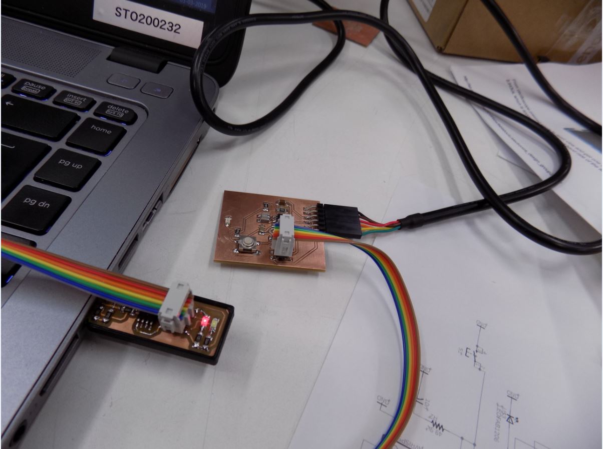
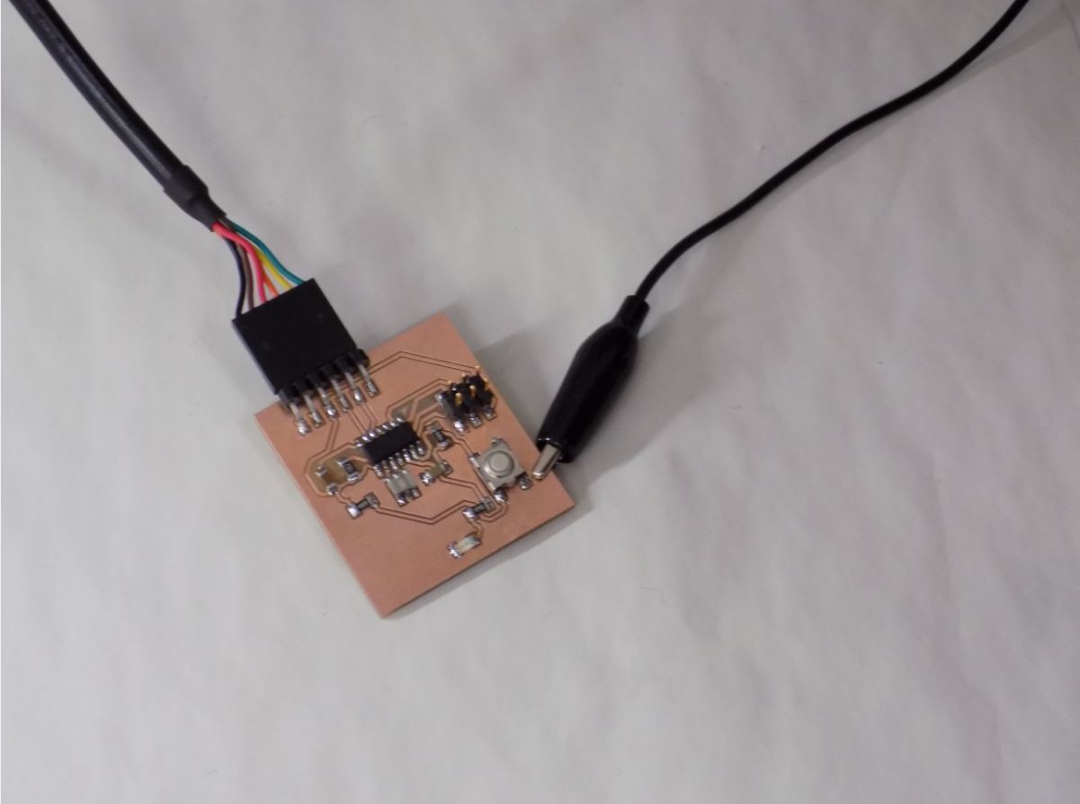
To program the board this instruction was followed. The ATTiny programmer that was made on Week5 was used to program. An ISP cable was needed to connect the programmer to the new board and ftdi cable (5V) to connect the new board to the computer.
First I also downloaded the c code and the make file needed.
To begin with the programming, I first opened GIT bash on the folder where I had stored my code and makefiles. While connecting the new board with an ISP cable make sure that the ground pins are matched. Then connect the new board to the computer with the ftdi cable and the red light will be turned on in the programmer.
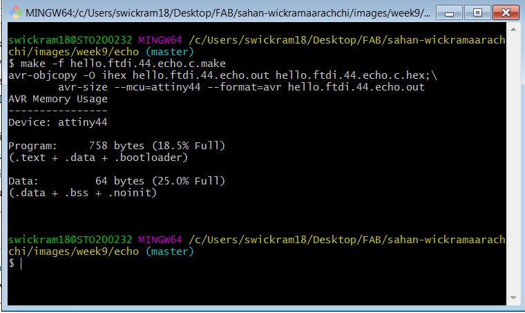
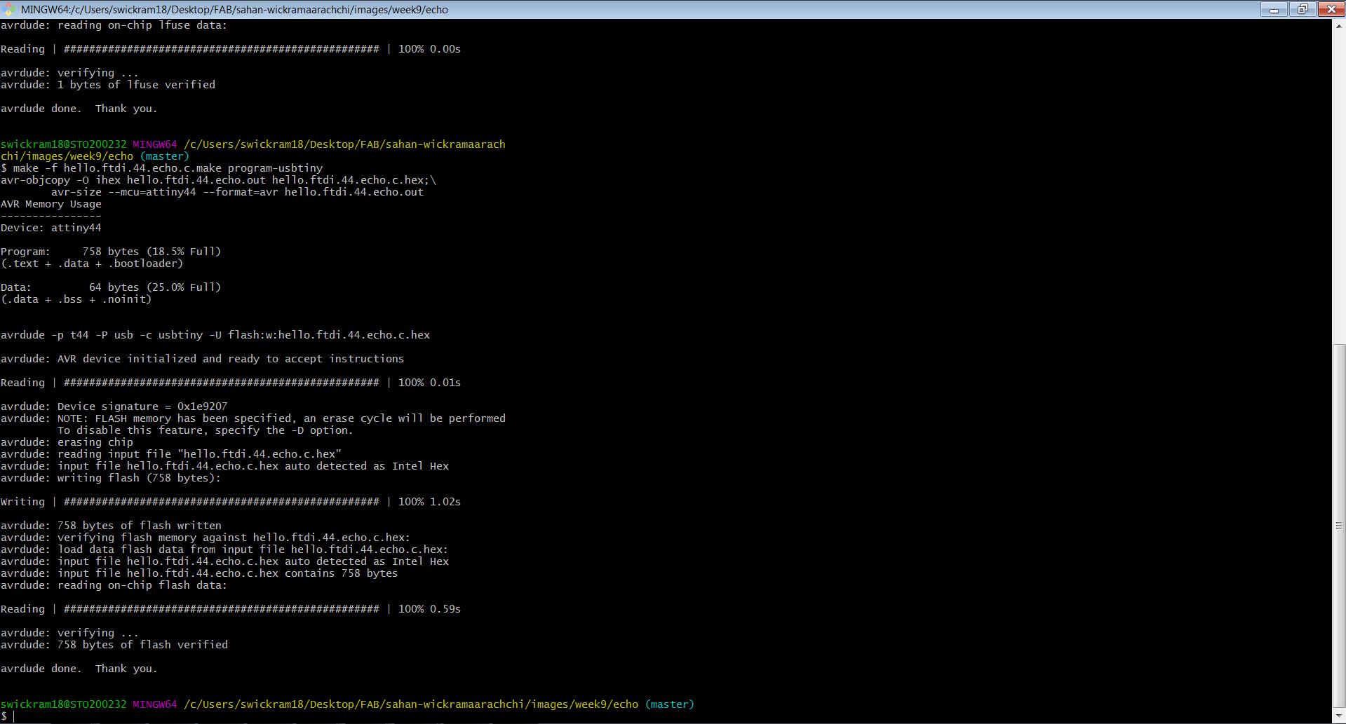
First, use the command make -f hello.ftdi.44.echo.c.make to make a .hex file for flashing in git bash.
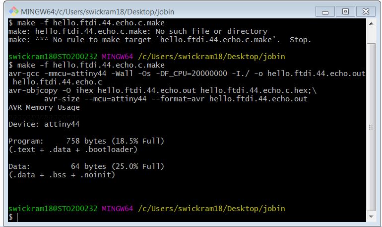
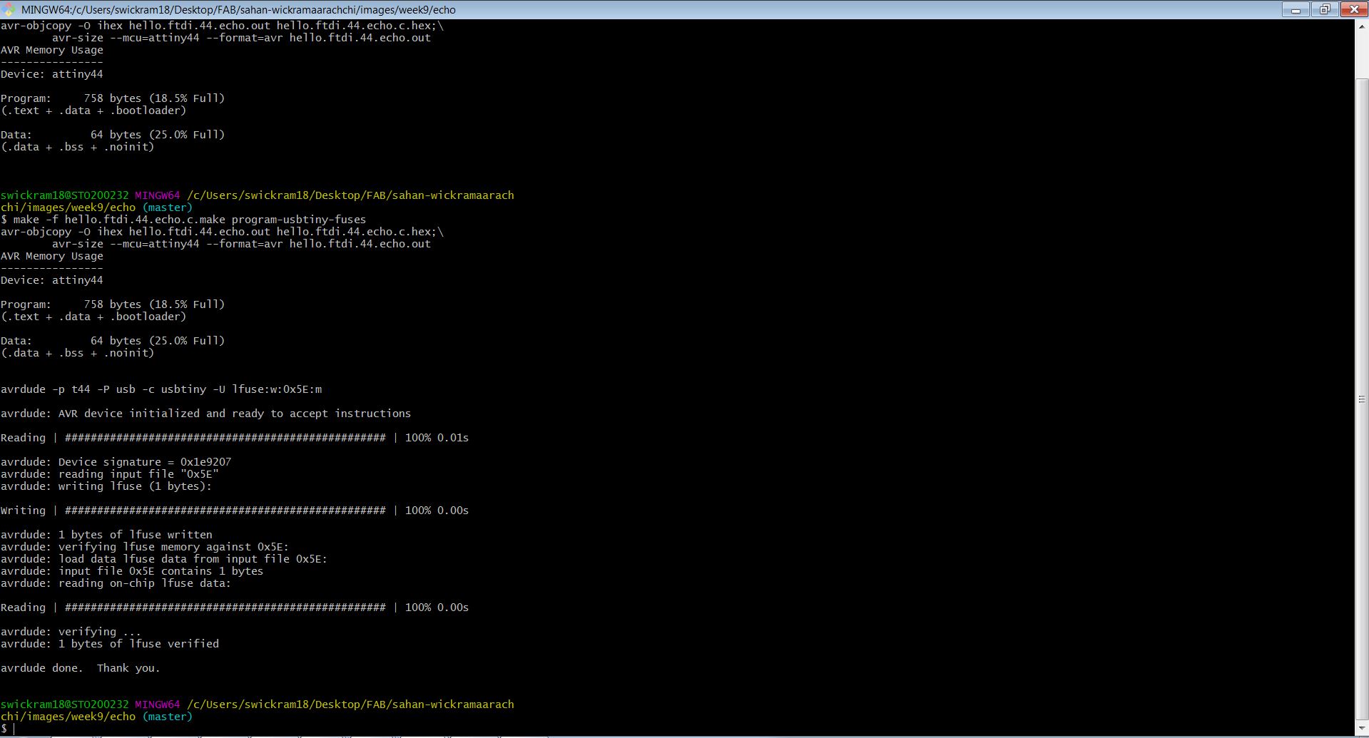
Then run the make fuses command make -f hello.ftdi.44.echo.c.make program-usbtiny-fuses . But I started getting error saying that device is not detectable.
However, as the group project, we were able to program Jobin's board. Same codes were used to program that and it worked.
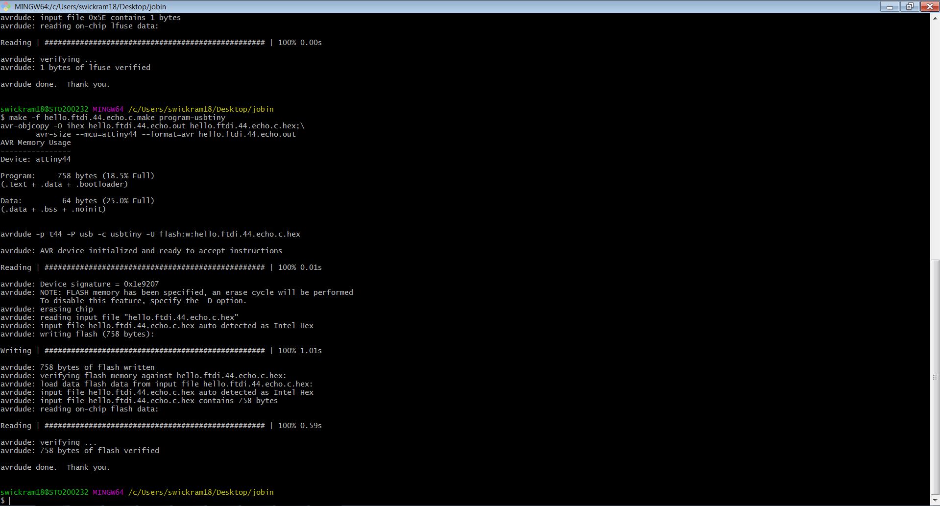
Finally we did the flashing of the developed microcontroller with the command: –make –f hello.ftdi.44.echo.c.make program-usbtiny—
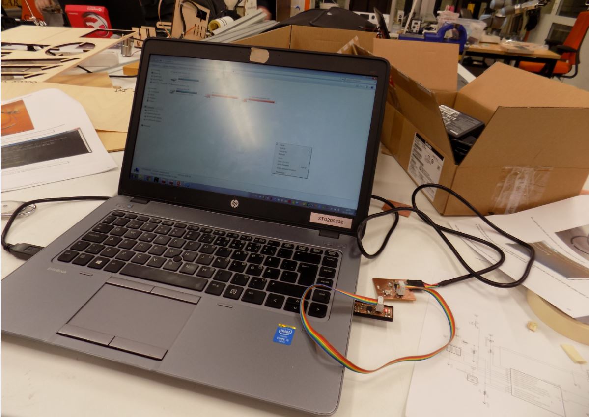
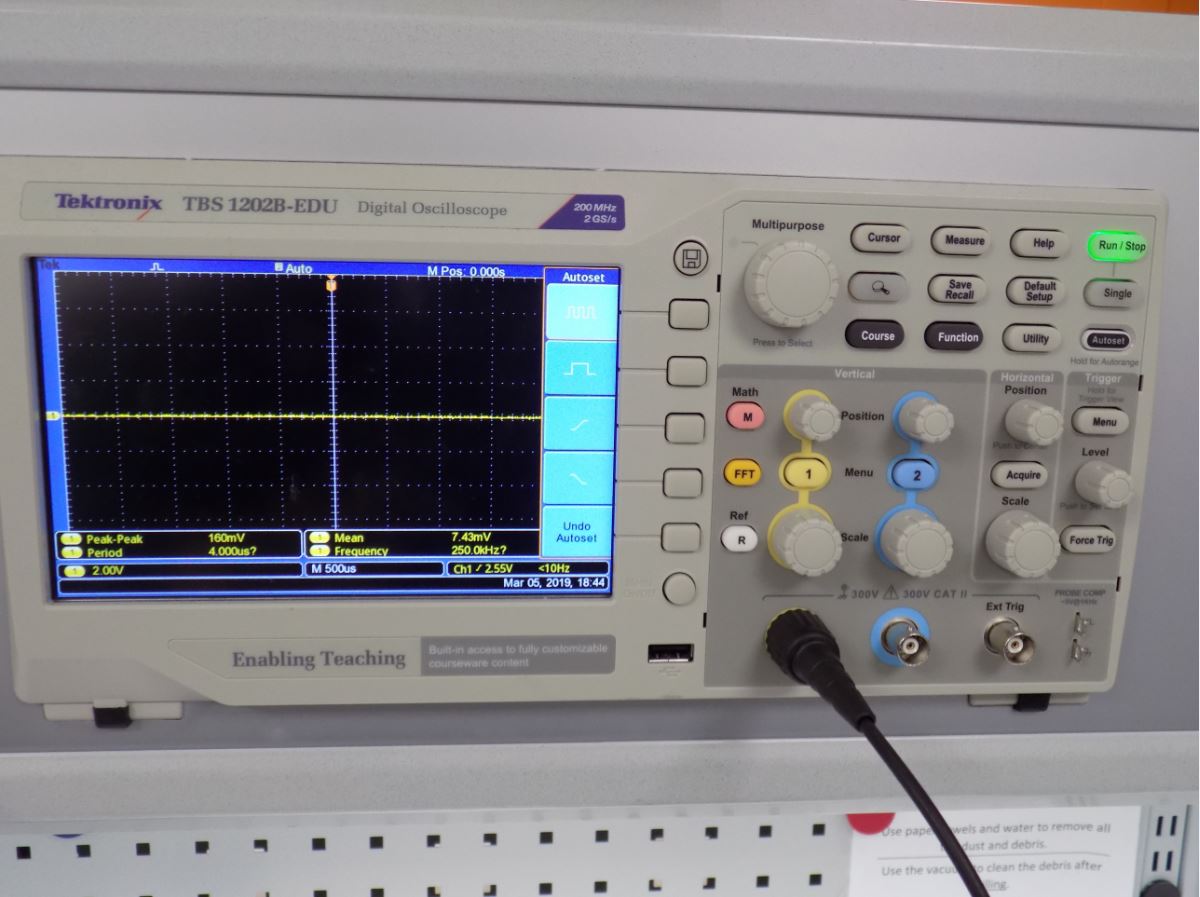
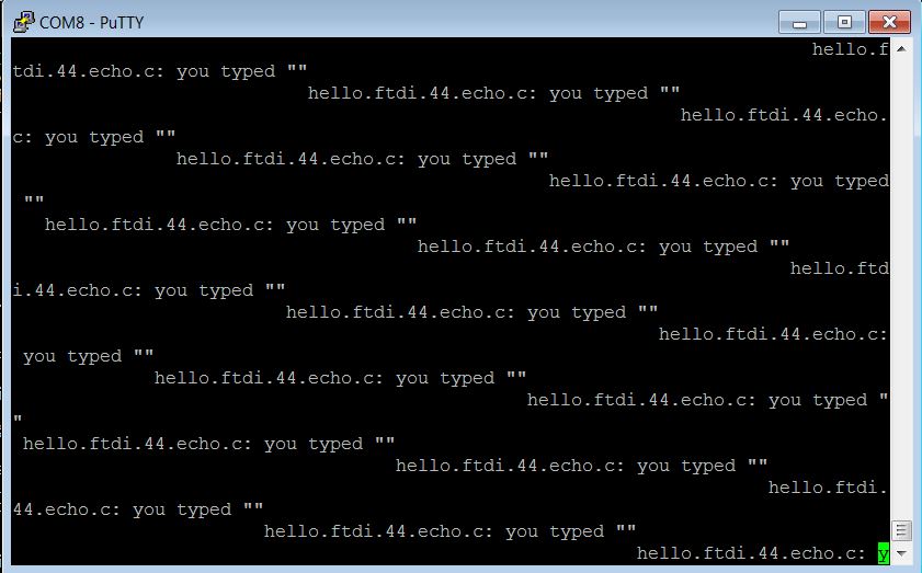
The group work for this week was to observe the operation of a microcontroller circuit board using an oscilloscope. We used Jobin's board for measuring the signal using the oscilloscope.
First We connected the ground plate of the board to the oscilloscope with black wire and the signal probe to serial input (4th in this case) pin.
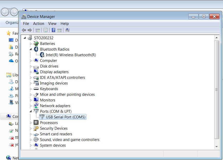
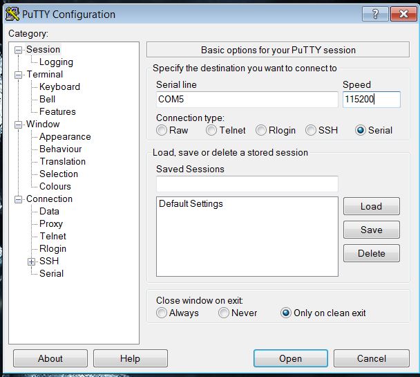
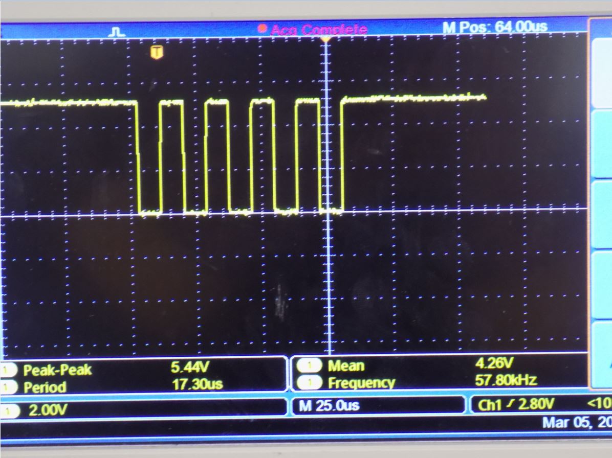
We used putty software to transmit data. To do that we need to check which COMport is connected to the programmer by going tocontrol panel>Device manager. After checking the COMport we open the putty and go to the serial menu. Then changed the COMport accordingly and put the baud rate as 115200 and pressed Ok.
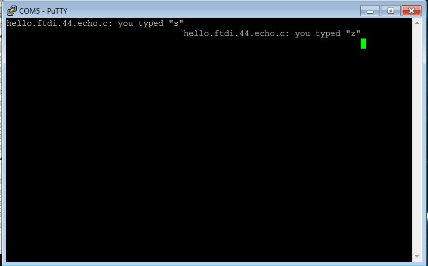
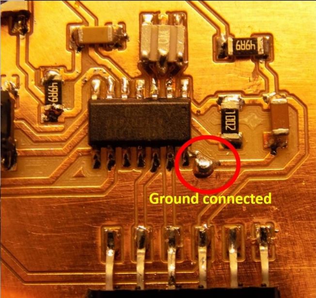
After giving some input on the terminal, unfortunately, putty window hanged and was slow displaying the signal. Our local instructor Antti helped to rectify the problem by finding that the IC ground was not connected properly. After soldering it to the nearest ground it started to work fine.
From oscilloscope, we pressed single to reset view and get one signal.
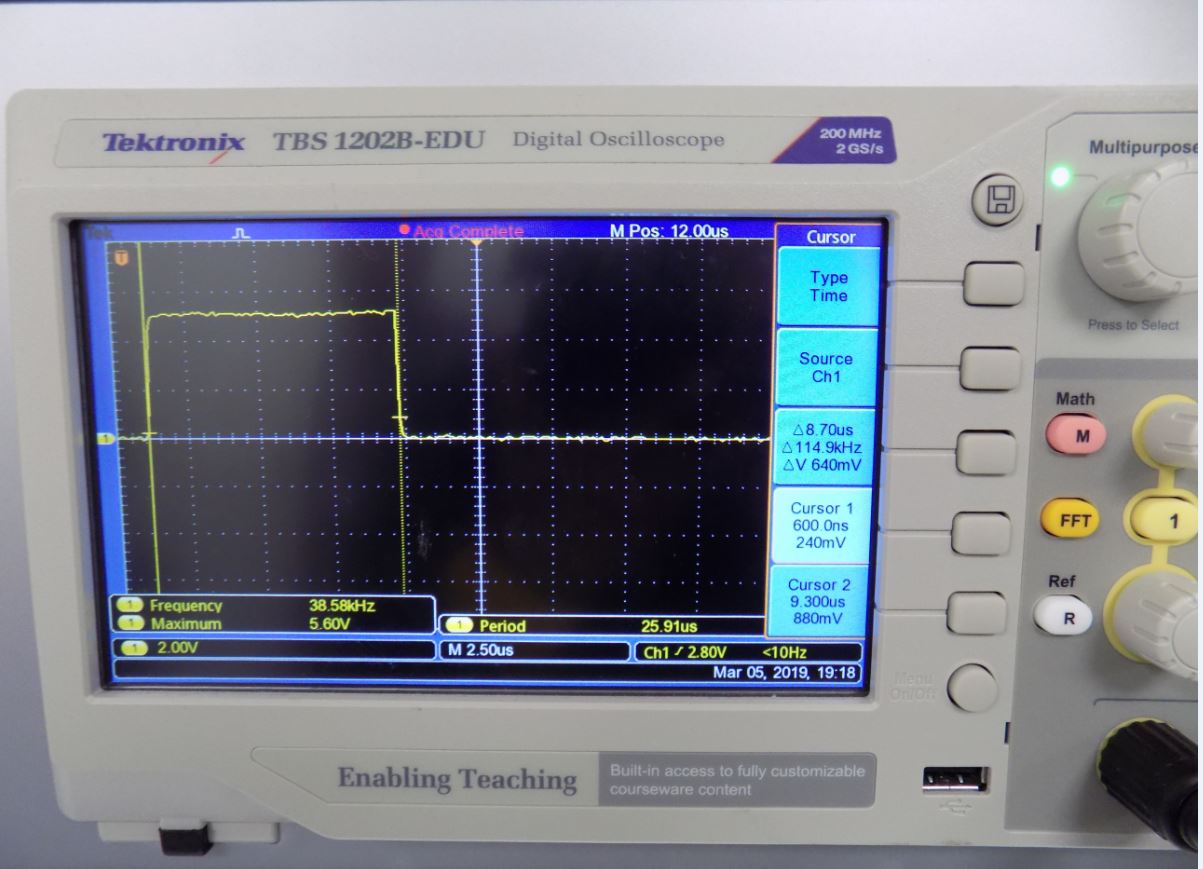
To see a bit from the oscilloscope as symbol sent we have to turn on the oscilloscopefirst and set it to single mode. Then after pressing a command eg. 'U' in the terminal on the oscilloscope view, we could see that pulse width was approximately 8,65us, which was close to the inversed baud rate of the terminal, 115200. Moreover, from the oscilloscope, we could count the bits
P.S.
I have managed to program my own board later after hours of trobleshooting. After checking each and every connection again with layout I decided to replace the Attiny 44A. After that the programming went smoothly.

Models files
Outline for the trace
rml file for traces
rml file for outline
Eagle layout file
Eagle schematic design file