Electronics Design
Week 6
Echo Hello-World Design
Review
This week’s goals are mostly, start with “Eagle” and understanding the basics of electronics design. The main goal is redraw a new version of the echo hello-world board, adding a button and a LED.
The first step is getting the software and the libraries of components to be able to redraw the board. Eagle (Easily Applicable Graphical Layout Editor) is a CAD tool used (among others) to draw schematics and printed circuit boards (PCB’s). Eagle is very popular around the world because of its freeware licenses and the availability of component libraries on the web.
We had the opportunity to learn some Eagle basics in our lab with a few physics students, but there are a bunch of resources all over the web to learn it. Get start with Eagle in this Fab Academy tutorial. Also download the hello-world board and schematic and the Fab Academy library here.
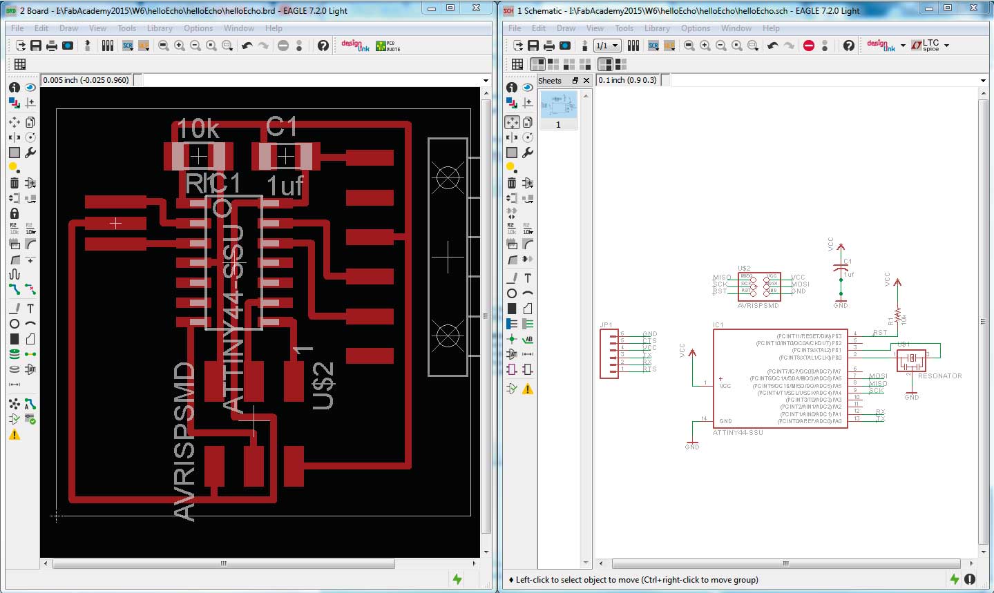
Firts Try
At the time to unzip the files and open it with eagle we will see the image above. Before start drawing we need to add the fab library in order to find the needed components. Depending on your operating system it’s necessary to paste the “fab library” on “Eagle libraries”. The possible route on Windows is C:\Program Files\EAGLE\lbr\.
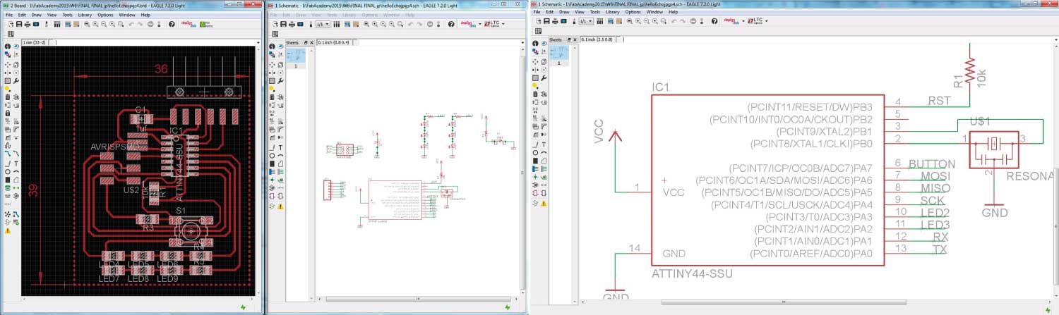
Eagle interface is quite simple to use. It is possible to easy switch between the “schematic” and the “board”. The schematic is a draw representing a circuit. It uses symbols to represent real-world electronic components. In the schematic we are going to add the missing components to complete the assignment. The board layout shows how the electrical components and traces will be laid out on the PCB.
The components already on the hello echo board are:
- 6-pin programming header
- Microcontroller: attiny44A
- FTDI header
- 20MHz resonator
- Resistor (value 10k)
- Capacitor (valeu 1uf)
I added the following components:
- (3) Red LEDs
- (3) Green LEDs
- (3) Blue LEDs
- (4) Resistor (value 1k)
- Button
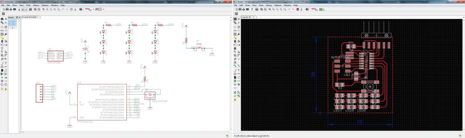
With all the components connected in the schematic I jumped into the board to start routing the traces of the board. I have to say that this part of the process was the most difficult for me. It’s a maze really difficult to solve. Trying to connect all the components without intersections was a hard job. I made some “adjustments” to be able to trace the routes easily but, I have to say that it was a decision that I regretted. Latter you will see...
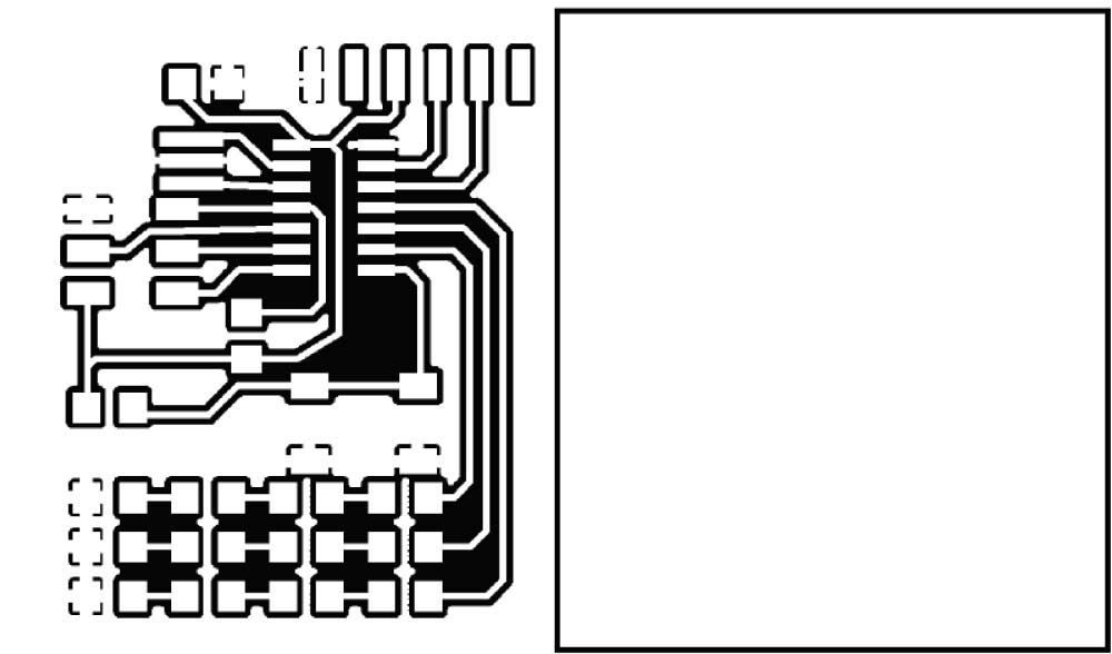
Firts Try Milling Process
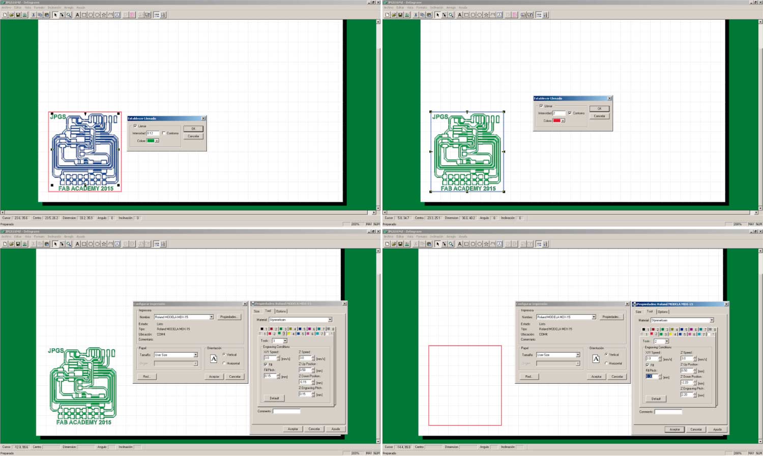
With the FabISP milling experience, I export the .bmp file and proceeded to milling in the Roland Modela. Turn off all the layers except the top layer. Go to File > Export > Image. Check the Monochrome box and set the resolution to 500 dpi. Click on Save as .BMP (Windows Bitmap File). Remember that our Modela Software Dr.Engrave only accepts .bmp and .dxf files.
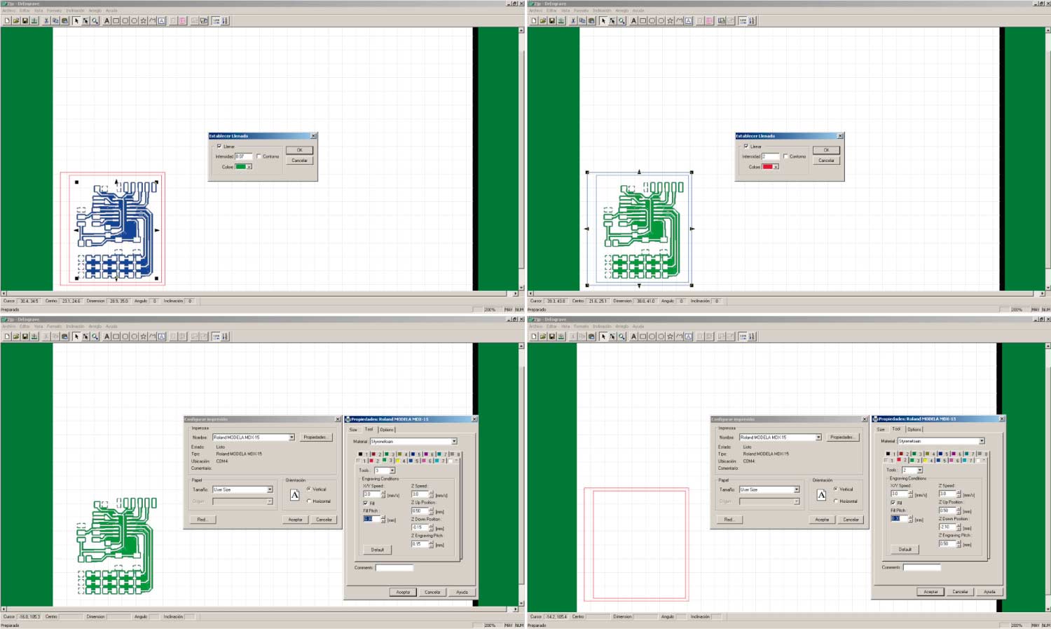
Millig Process
- >Fill Intensity: 0.07 - Green
- >X/Y Speed: 3.0 mm/S
- >Z Speed: 3.0 mm/s
- >Fill Pitch: 0.30 mm
- >Z Up Position: 0.5 mm
- >Z Down Position: -0.15 mm
- >Z Engraving Pitch: 0.15 mm
Cutting Process
- >Fill Intensity: 2 - Red
- >X/Y Speed: 3.0 mm/S
- >Z Speed: 3.0 mm/s
- >Fill Pitch: 0.30 mm
- >Z Up Position: 0.5mm
- >Z Down Position: -2.10 mm
- >Z Engraving Pitch: 0.50 mm
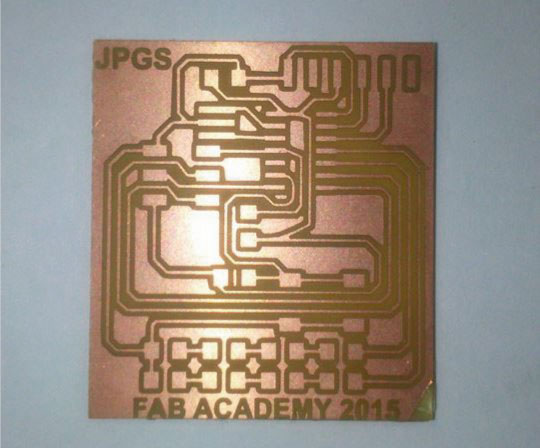
As can be seen in the image bellow the result was not really good, due to a series of “parameters” that I didn’t took in account. The first one was the width of the traces. The default number is 0.4064 mm, try to keep it that way. The second one was the fill intensity to mill in the Roland Modela. I used 0.07mm, but the optimal is 0.12mm and for the last one but not less important, the resolution of the .bmp exported image. I used 500dpi but its better to have better resolution images for the milling. Set it to 2400dpi.
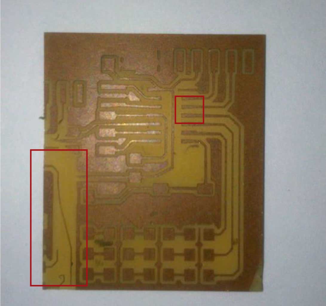
Wrong Conections
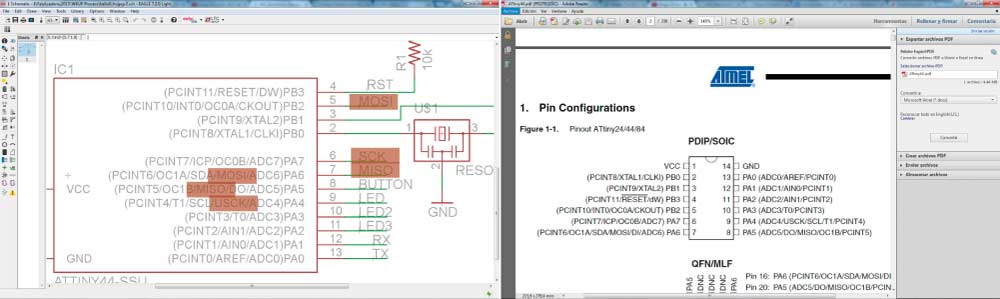
As I told before the “adjustments” I made on the pins of the microcontroller to trace the routes easily were WRONG. Although I checked the DATASHEET I have to admit I didn’t understood it. I used pins to connect the LEDs that CAN`T be used because they are specific for data input and output (MISO, MOSI, SCK). Now I know that pins have specific functions and can understand a little bit the DATASHEET.
Second Try
I corrected all the wrong connections and started all over again having in mind all the preview mistakes. I erased a series of the LEDs. The final added components were:
- (3) Red LEDs
- (3) Green LEDs
- (3) Resistor (value 1k)
- Button
Second Try Milling Process
The resolution value for the .bmp file was 2400dpi. This is really important at the time to import the image in the machine software.
These were the parameters for the milling and cutting process:
Millig Process
- >Fill Intensity: 0.12 - Green
- >X/Y Speed: 3.0 mm/S
- >Z Speed: 3.0 mm/s
- >Fill Pitch: 0.15 mm
- >Z Up Position: 0.5 mm
- >Z Down Position: -0.15 mm
- >Z Engraving Pitch: 0.15 mm
Cutting Process
- >Fill Intensity: 2 - Red
- >X/Y Speed: 3.0 mm/S
- >Z Speed: 3.0 mm/s
- >Fill Pitch: 0.30 mm
- >Z Up Position: 0.5 mm
- >Z Down Position: -2.20 mm
- >Z Engraving Pitch: 0.55 mm
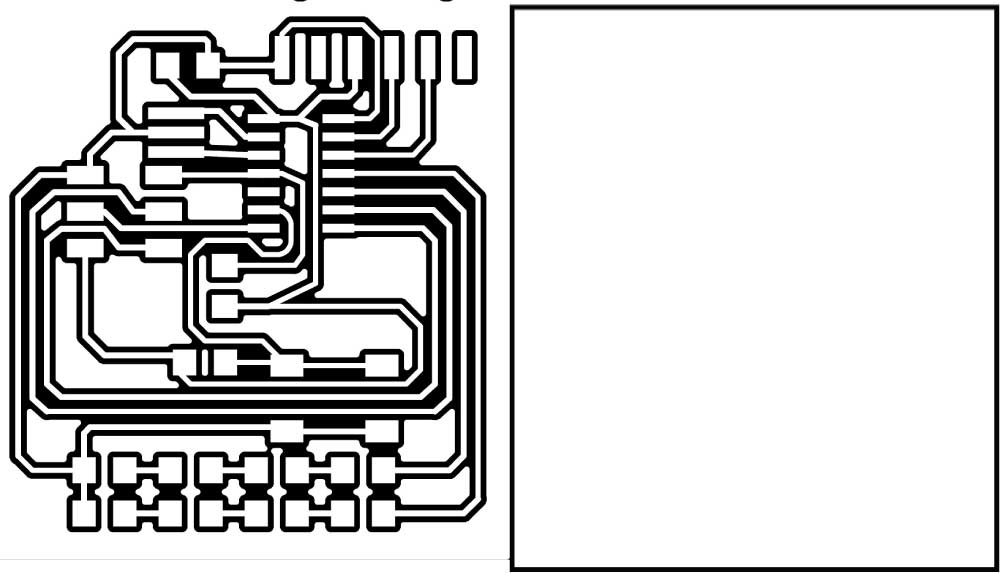
This time the result went much better, very clean and well defined. The adjustments in the width of the traces, the proper distance between them and the resolution of the image are fundamental to get a good end result.
Echo Hello-World Soldering
I felt much confident soldering the components in this board and could accomplish the task with good results. The practice is playing off. Some of the components are a little bit difficult to solder than the others but in general it’s the same process. Start soldering the most difficult components (like the microprocessor) and continue trying to keep a “soldering order”.
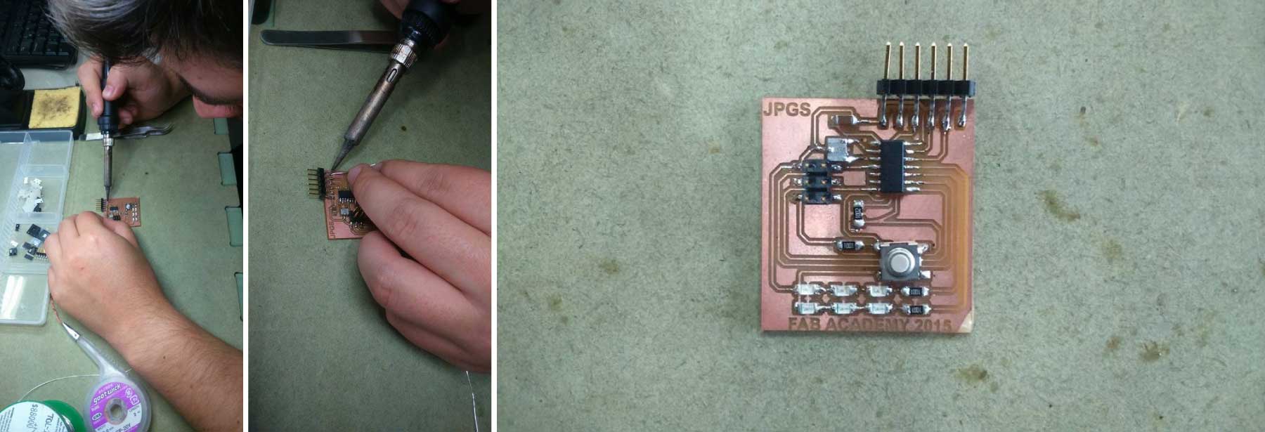
This week brought a lot of things to learn; new software that will be fundamental in the next weeks, a lot of adjustments in the PCB's fabrication process and a bunch of new knowledge in electronics. The board is ready to be programmed the next week, hope everything works.