|
Week 6: Electronic design
This week assignment was about designing and fabricating an electronic board. Then the components should be soldered on top of the board. We did not have to start from scratch. We should redesign a board by adding an LED and a button to it.
Redesigning the board
For adding the LED and the button to the former design I followed the tutorial on Tutorial for redesigning the board
In step 2 of this tutorial, there is a link for downloading the former design which called HelloEcho. In the HelloEcho folder there are the HelloEcho.sch and HelloEcho.brd files which the first one is the schematic file and the second is the layout file.
I used EagleCad to redesign the board. First I installed EagleCad, installed the libraries which where addressed in the tutorial and put them in use. Then I opened the HelloEcho.sch
Opening the .sch file the .brd file will open too. Using the add button I the LED, the resistor, the switch, the Vcc and the CND and connected them as they should be connected. Then I checked the electronics rules by clicking on the ERC button. I did not get any erros but I got several warnings.
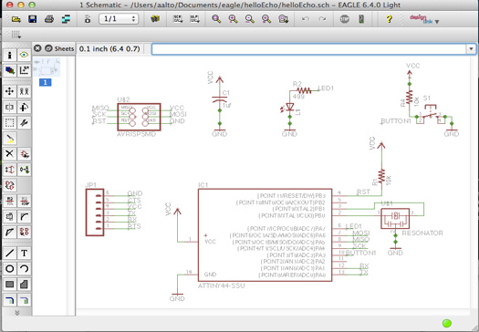
The schematic view
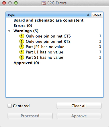
ERC check
Then I switched to the board view to do the layout. Here I tried to use the Ripup tool to ripup routed tracks to air wire. After that I placed all the new components which are located on the left lower corner of the view inside the board area. Clicked on the Rastnest button which gives the shortest possible air wires and started to do the manual routing.
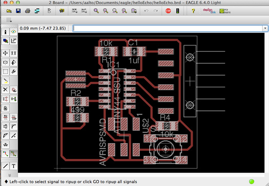
The board view
To check the design rules I clicked on the DRC button and then check. I got some clearance error. Because the clearance was set to 16 mil, but I had my traces in some parts closer than that. Clicking on each error on DRC dialogue box, the location of the error is visible and then it is easy to fix.
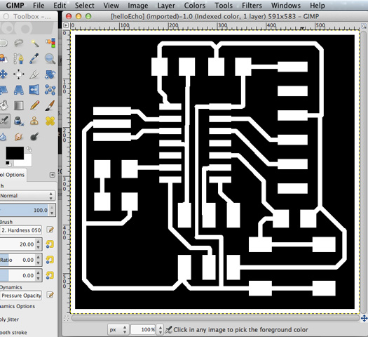
Having the board layout ready I selected the top layer and deselected the rest of the layers to have only the traces. Then I exported as PNG.
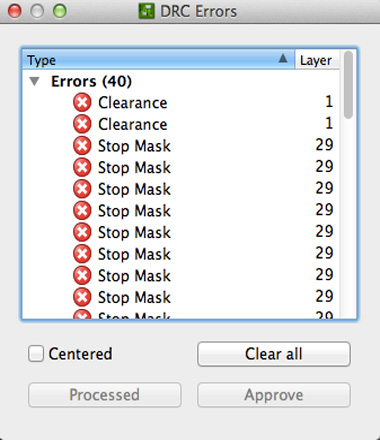
Primary DRC check
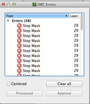
final DRC check
Preparing the png files using Gimp
I used Gimp to modify the board and make the interior. In the tutorial mentioned above the steps are explained. First I downloaded Gimp and open the HelloEcho.PNG there. I cropped the unwanted part and exported as a .PNG file. For making the interior, following the tutorial, Modify menue > Canvas > Canvas size, add 20px to the width while the proportions are linked, hitting the "center" button and then going to the image > flatten image will make a 20px white boarder around the board trace image.
I saved as another file and used the bucket fill to fill the traces (Tools > Paint tools > Bucket fill). After this step I had a black image with white traces around it. To invert it I went to Colors > Value invert and then I had a white image with black traces around it which was suitable for cutting the board interior. I exported it as PNG and I had both traces and interior ready.
The traces
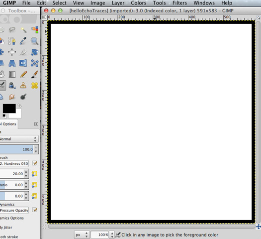
The interior
Soldering the components
I did not have the exact FTDI connecter which I had used the foot print for, therefore I used the standing connecter.
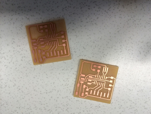
PCBs
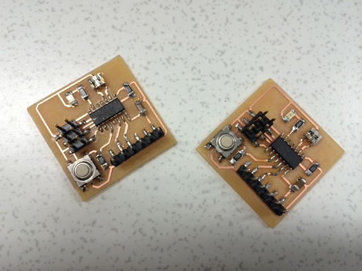
The final boards after soldering the components
Files:
LED-BUTTON
|
 Fab Academy Class 2014