Installing the Software
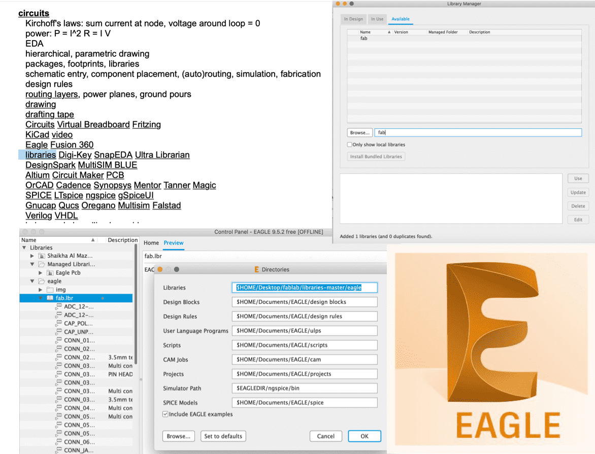
- Using my Autodesk account, i installed the software version for mac through Eagle Webiste.
- Then I installed Fab Lab library from Electronic Design Page. This is a very crucial step since we need to make sure that the board will fit the components that will be used and available in fablab, in other words to get most of the footprints of the SMD components that we have.
- Adding the library can be done from the control panel going to the directories and pasting the path of the fablab library that was installed in the first tab "Libraries". Then in the library manager we can search for "fab" which is the name of the installed library and use it to add components.
Board Components
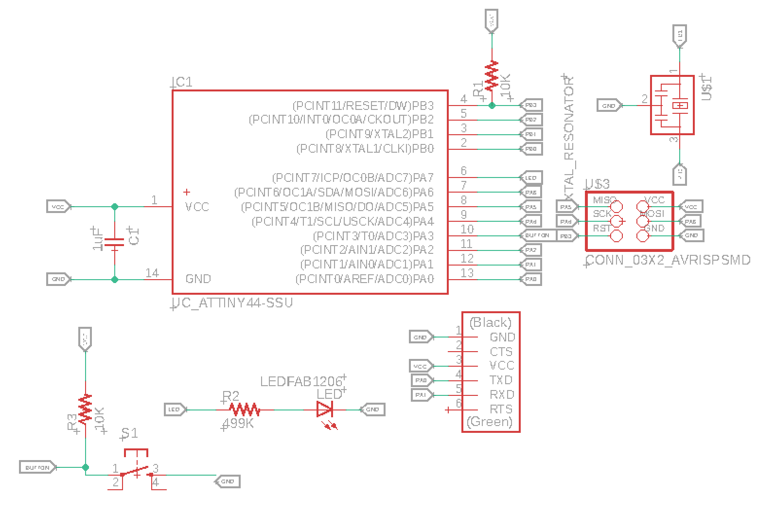
- Attiny 44_SSU
- FTDI Connector: CONN_06_FTDI-SMD-HEADER
- ISP Header: CONN_03X2_AVRISP
- 10K ohm Resistor: R1206FAB
- 1K ohm Resistor: R1206FAB
- LED: LEDFAB1206
- 499 ohm Resistor: R1206FAB, The LED used has a IF=20 mA with V=2.4v and the Attiny44 output high is 4.3V according to the datasheet, so the required resistance will be 5-2.4/20m = 130 ohm or greater so I used the minimum resistor that is close to this value which is 499 ohm.
- Resonator: XTAL_RESONATOR
- 1 uF Capacitor: CAP_UNPOLARIZEDFAB
- Push Button: SW_SWITCH_TACTILE_6MM
The Schematic
- The first step is to create a new project then to create the schematic.
- Then components footprints are added.
- Then electrical connections are made between the components.
- A very helpful technique that will help in keeping the schematic neat and easy to read is adding name tags to wire ends and pins on the microcontroller making sure they both have the same name, this is done instead of wiring all connections physically, which will result in having traces connecting those ends in the Board layout.
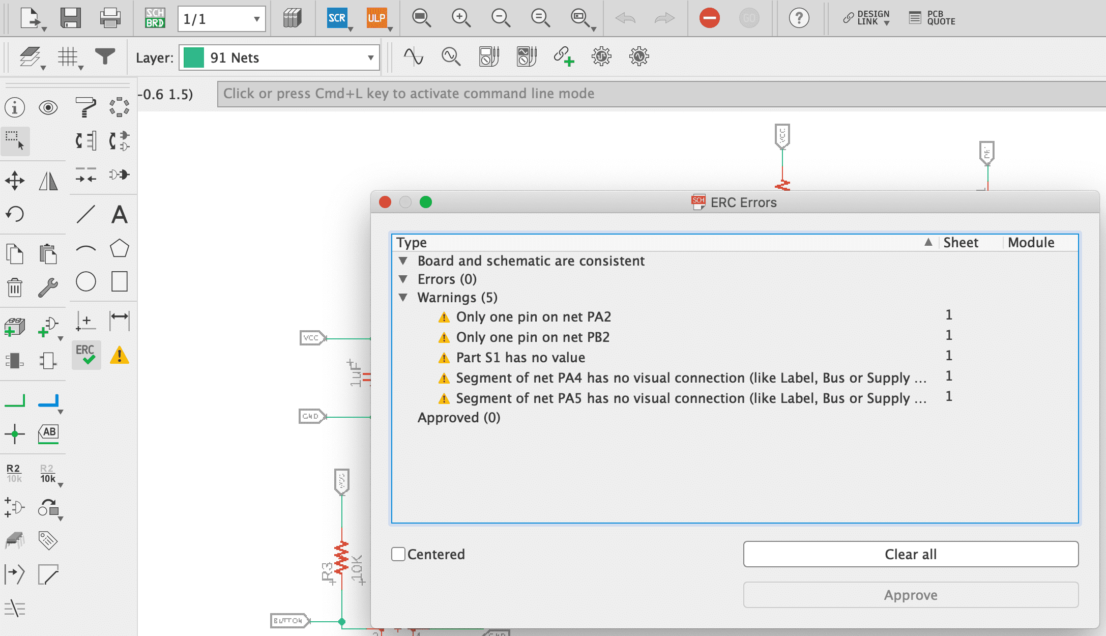
- After finishing all connections, a very imposrtant step before moving to the board design is to look for the errors and rectify them, using ERC command, it will also indicate where exactly the error is which makes it very easy to navigate through.
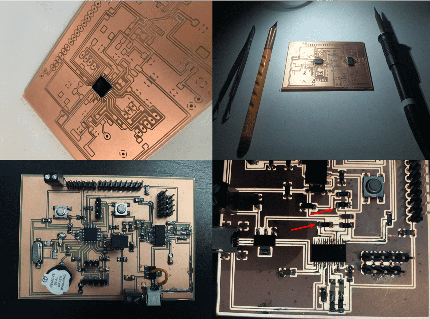
The Board
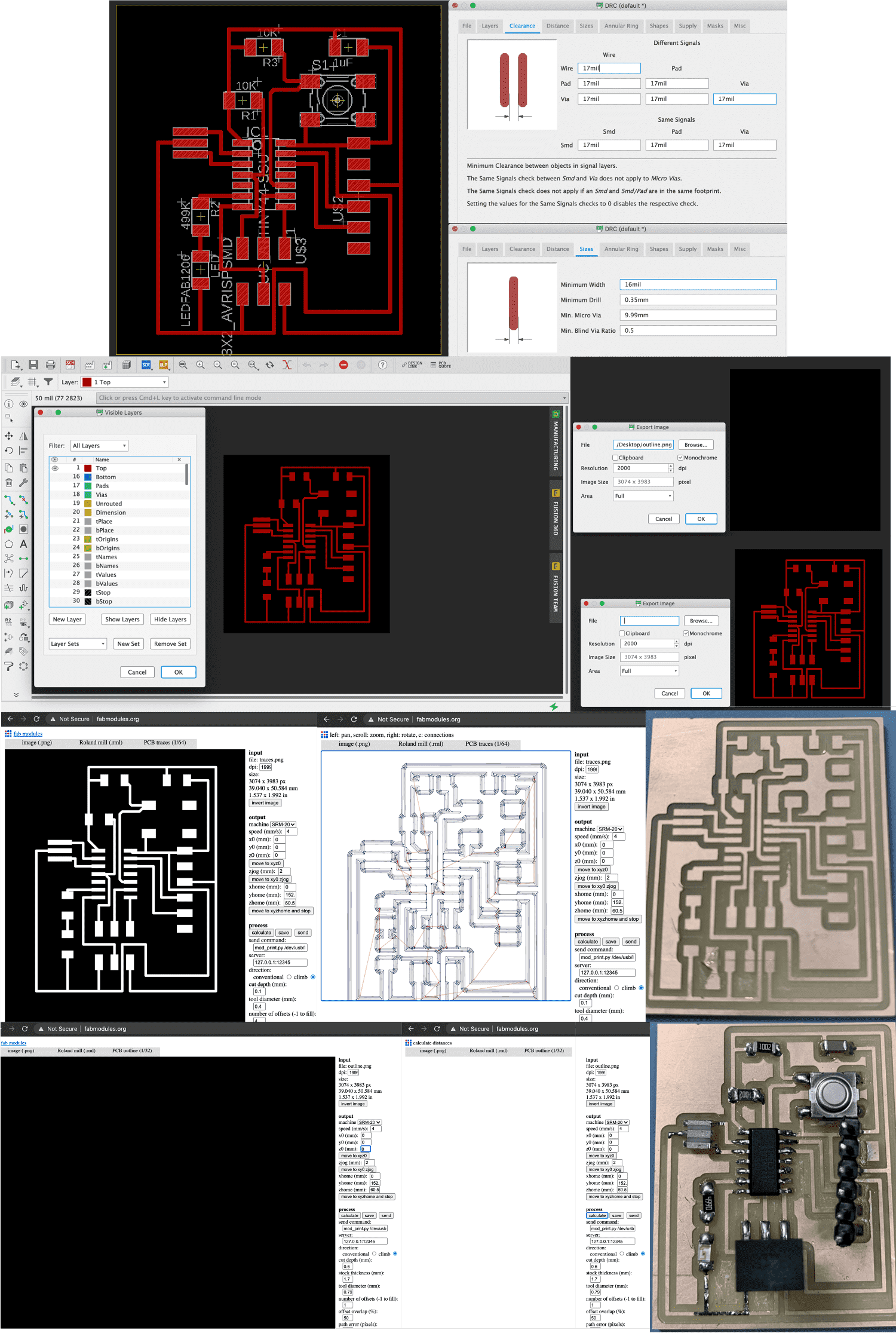
- After finalizing the schematic, the board needs to be done by going to File>Switch to board (or by just clicking on the icon)
- Before starting with the wiring process, some parameters related to spacing needs to be modified, this is done by choosing the DRC icon (Design Rule Check). We were instructed to just change the clearance and sizes as per the milling bit available (since previously in fab modules, we used 1/64 inches for traces and 1/32 inches for outline, so we take the smallest 1/64 inches which is close to 17mil, since the conversion from inch to mil is 1000).
- Wiring starts by first distributing the components and changing the orientation putting in mind the connections and how close they are, of course the wiring needs time until you reach the optimum connection, also how big the board is matters, the smaller the better.
- Again, after finishing all connections, ERC command must be used to look for the errors and rectify them.
- When the board is ready, it is exported twice, one for traces and one for outline.For traces, we go to the layers option and we hide all layers except the top layer (red), for outline we hide all layers since we just need the size of the board.
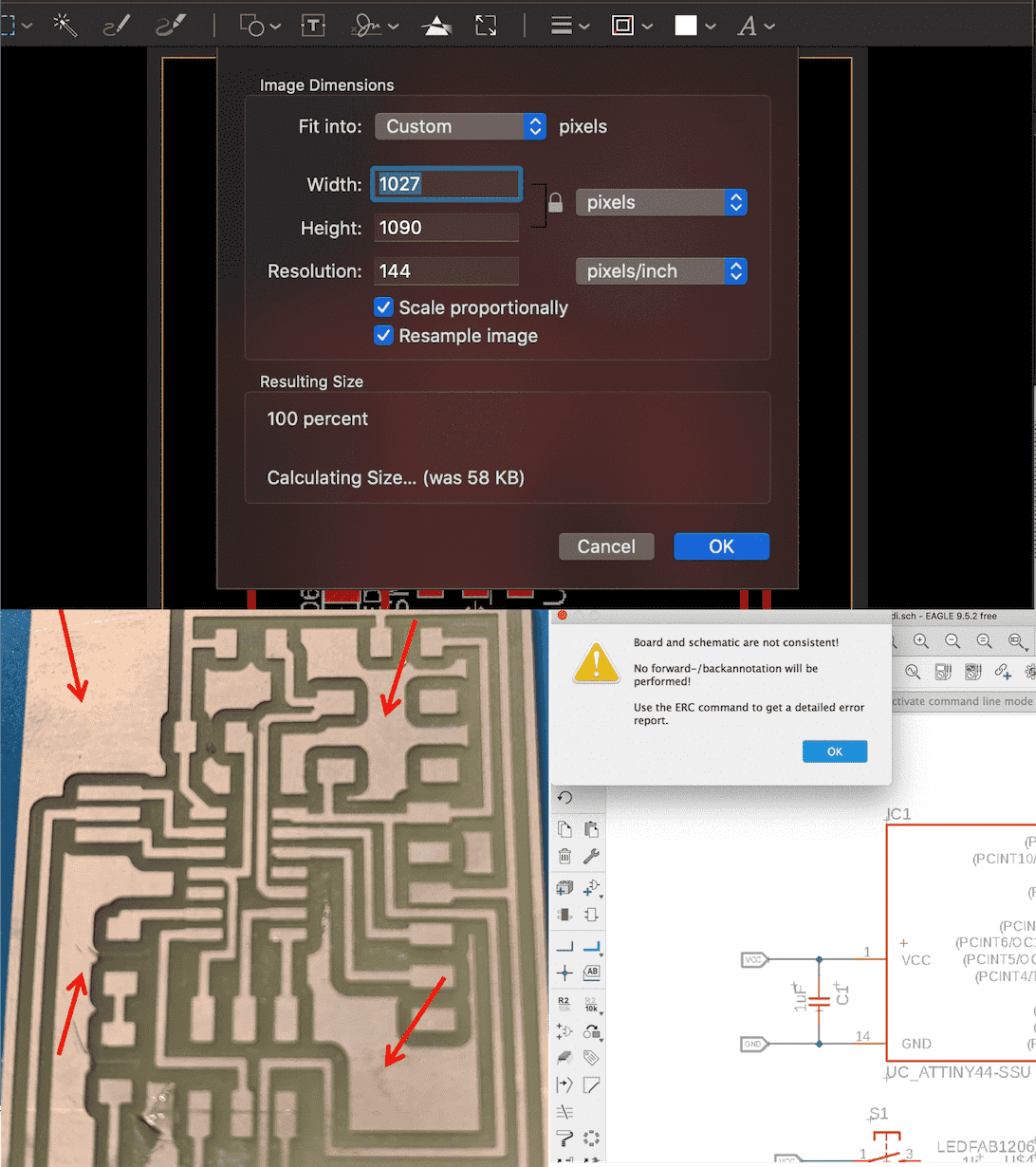
- For exporting, we go to File>Export>IMG. Dpi must be increased to maximum, i used 2000. For exporting the traces, monochrome option must be ticked. Also, the size of the image should be known for future verification.
- After that, the steps used in the previous week are followed:
- Exporting the images from Fabmodules.
- Milling the board.
- Soldering the components.
- Using multimeter to check for short circuits.
- The board is now ready to be programmed!
- To check the functionality of the board, a simple code was made to check that, and the code used is explained in the Embedded Programming Week.
Downloads
Issues faced
- After finishing the board and schematic, i found an error that kept showing several times, which says that the board and the schematic are not consistent.Also, not all components were synced correctly in the board. So i did the manual connection using signal icon on the tab to relate the components before wiring. In addition to that, some names on board were different than the schematic which just required unifying the names on both schematic and board.
- After exporting the traces and outlines from eagle, and using them in Fabmodules, I discovered that the size is doubled, i tried to change the resolution setting as my colleagues used to do in Windows, but it didn't work. Luckily in Mac we can resize the images directly from the Preview App, and thus i reduced it exactly 50% using the original size shown in eagle when exporting. It worked just fine with the rest of my colleagues who used Mac since we all faced the same issues.
- When i printed the board, i noticed that the unused area wasn't removed during the milling process. After asking my instructor, i came to know that the offset in fabmodules in traces can be changed from 4 to -1 which will solve it but it will require more time. Etching wasn't required though it was just a matter of keeping the board presentable.
Using Another Software For The Circuit
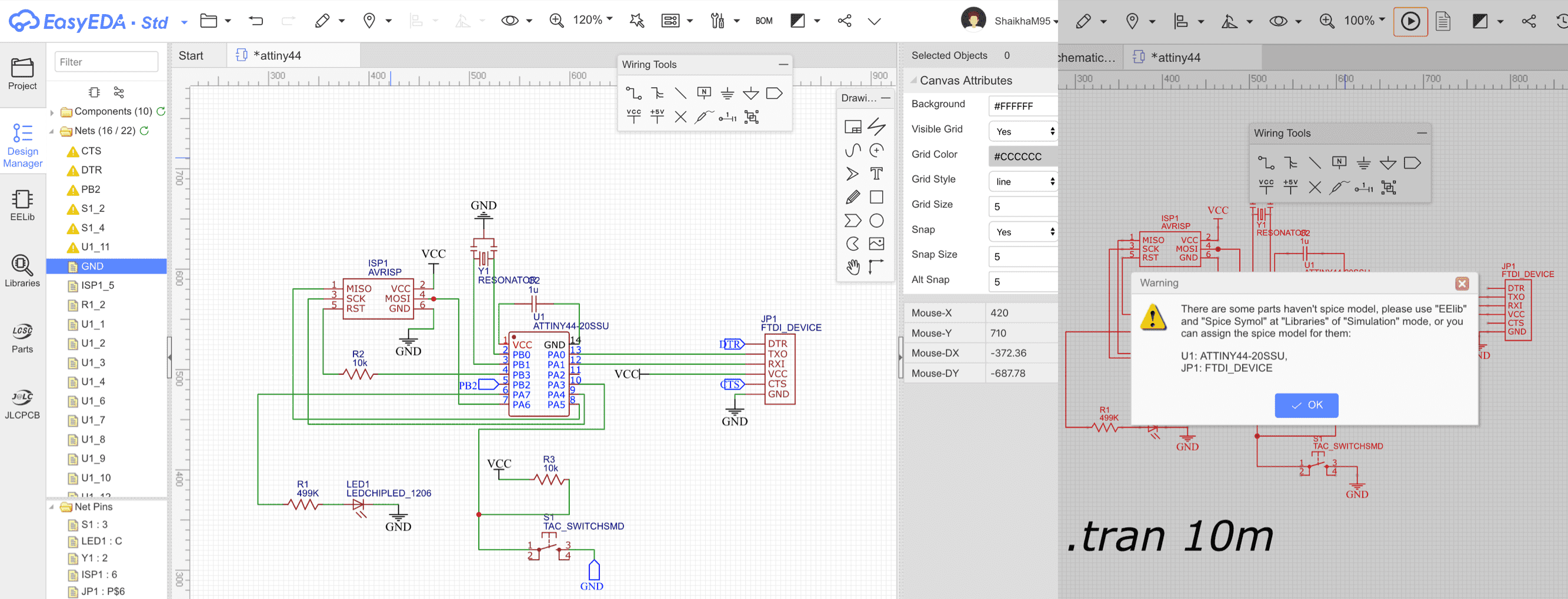
Since i'm using a Mac, most of the softawres that i used to use in the previous years couldn't be installed since they are only compatible with windows, such as Circuit Maker & Multisim which have simulation option. So i searched and found a software called EasyEDA that also have simulation. I did give it a try even though it was very hard to look for the same components footprint for fablab, but since it won't be printed, i just proceeded with what i found. After finishing the circuit connections, i tried to run it for simulation but got stuck on an error, i will try to figure it out soon.
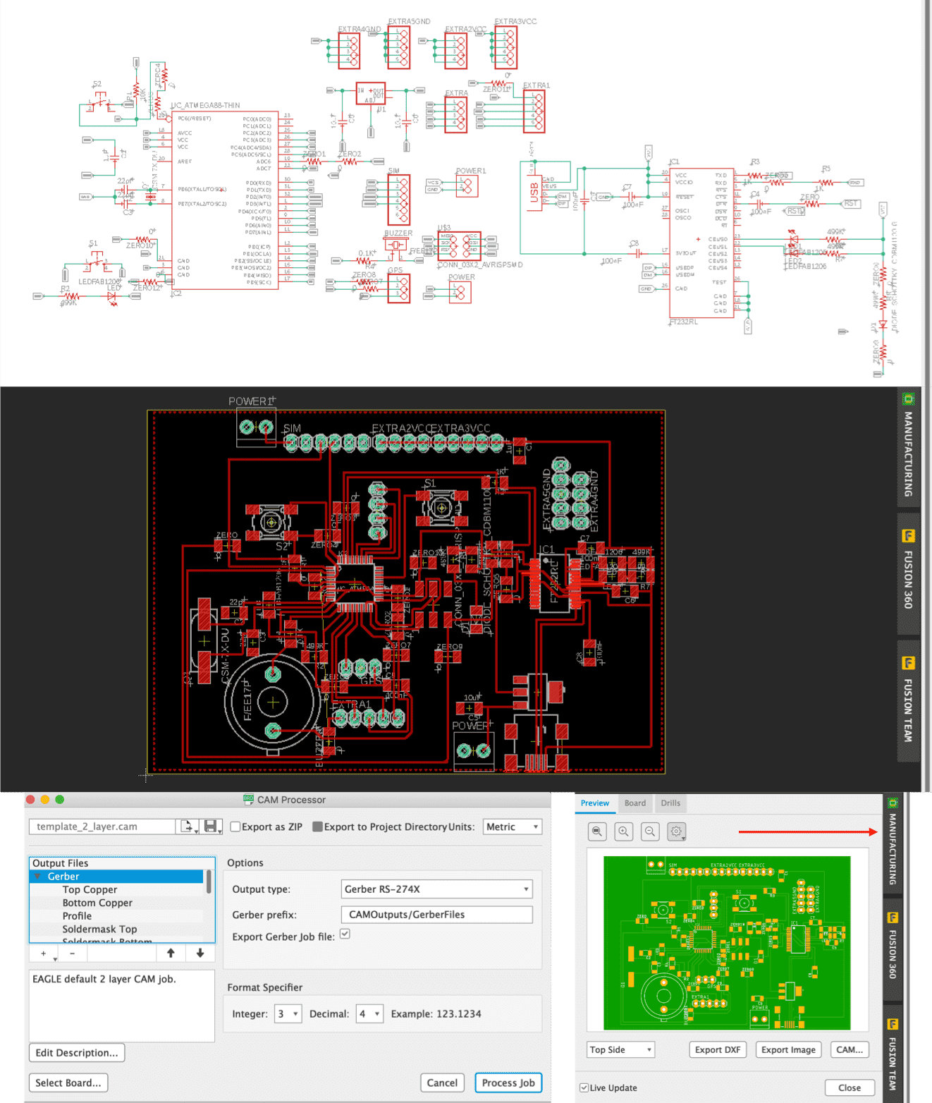
Board #2
- Atmega 328 (in schematic we used atmega88)
- FT232RL
- Crystal Oscillator
- Buzzer
- GPS
- SIM module
- LED
- Resistors
- Capacitors
- Diode
- Headers
- Power Terminal
- USB mini
- Switch
Downloads
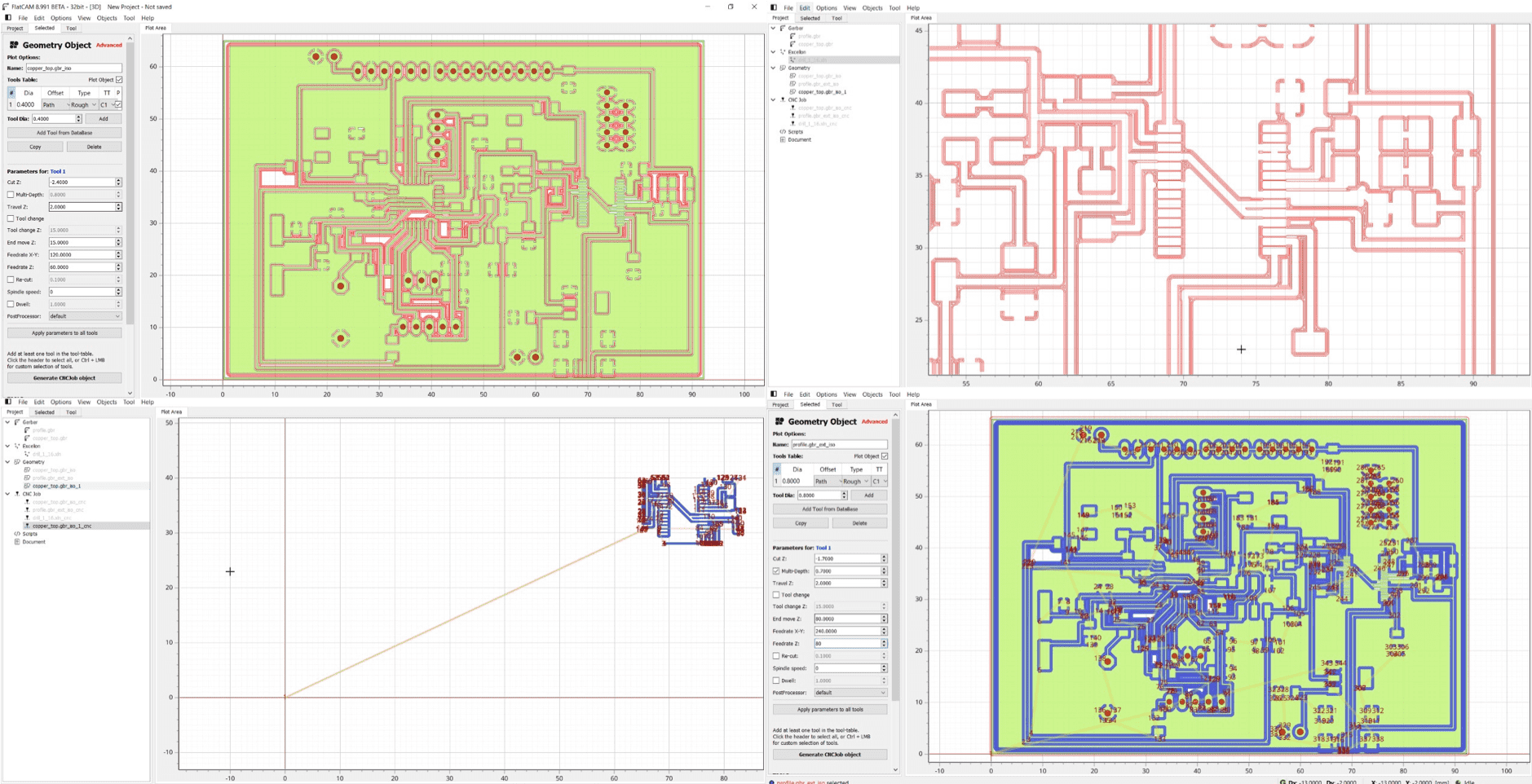
Flatcam
FlatCAM is an open source software used for milling bordas. It can open Gerber, Excellon or G-code, and gives the option to either edit it or create from scatch, and output file in the G-Code format. It also offers isolation routing and can visualize the pcb to know exactly how the milling machine is going to make the PCB.
For milling my PCB, i had the following sequence: Traces, FT232RL, Drilling and cutting profile. The traces are for creating the path, routes and padding for the pcb using 1/64 milling bit. The FT232RL since it has tiny legs, i used the isolation mode to only mill that part after the main traces using 1/128 milling bit. Then for the headers and cutting the outline, drilling was used.
One point that i need to mention is that Flatcam wasn't installed on my Mac, and i found out that many users faced the same problem, so i had to use windows to use flatcam.
Soldering & Debugging
Group Assignment
- Logic Probe: easy to use forms of digital testers being able to test logic levels (boolean 0 or 1). It is straightforward, i connected the LED and placed the probe to check the status whenever the LED turns on and off.
- Oscilloscope: a type of electronic test instrument that graphically displays varying signal voltages,the displayed waveform can then be analyzed for properties such as amplitude, frequency, rise time, time interval, distortion, and others.I connected the LED again but this time i changed the blinking time to be fast so that we can observe it on the oscilloscope.
Experience
Creating a circuit from scratch using Eagle was an interesting experience as it was my first time, but i had previous experience with making circuits using different softwares, which made it easier for me to use.