|
Week6: Electronic Designs
Ok, lets learn something more
about the apassionate world of electronic :)
My
goal for this class is to learn if the electrons moves along the wires
when i turn on the light or they only vibrates in an stationary
way...if someone could answer this question, please light my way :P
Modify an electronic circuit
The
first thing we must do in this week schedule is redraw a pcb to add
some components. Again, my skills in electronics are null, but at least
i learn to solder two weeks ago.
Im gonna use Eagle as the
software to do a schematic and generate the pcb files needed to do with
the Modela. First install the Eagle
software,
that comes in a Free version (with some pcb size limits). At
installation times ask wich license you have...obviously, we are going
to use the free version (no freemium version, Free).
First thing i do is try to start
from scratch, just following the Hello.ftdi.44
board. Open the file and make a list with the components, and
their name in the libraries of the Eagle:
- XTAL1 20Mhz (named CRYSTAL)
- R1 10k (RES-US1206 or
RES-US1206FAB)
- C1 1uF (CAP-US1206)
- ATTINY44 (ATTINY44-SSU)
- J2 FTDI (FTDI-SMD-HEADER)
- J1 ISP (AVRISPSMD)
and
- SWITCH (6MM-SWITCH)
-LED (LED1206) this is
inside the 01_fab_hello library
- R2 499k (RES-US1206)
- R3 10k (RES-US1206)
After
having all the components localized, we need to open the Eagle and see
if this components are at the libraries of the software. For this week
we have the fab.lbr
file, right next to the Eagle link. We download them and start to work,
although i recomend download all
the libraries
ready to download a the Provicence Fab Academy web, inside the link
"tutorials" and inside "07-electronics Designe" (a really useful web
site fo rthe students at Fab Academy). When we have the library file
stored in our pc, then we must copy this file in a directory of the
program. In every operating system is diferent, so you could search for
a folder called "lbr"...not a usual name. In this folder we put all the
.lbr files (that contents the libraries of the components we could use).
If you want to know in which folders are stored the
libraries or the proyects, you can ckeck it at the Control Panel, in
Options -> Directories...
Once you libraries are inside the correct folder, you could decide
which libraries are "active" in every proyect you start. In the Control
Panel of the Eagle, we could find a "libraries" tree. Im going to use
only the Fab Lab libraries, so right click in "libraries" and select
"Use none". Then make a single click in the small dot at the right of
the libraries to activate them.
When we add a component in schematic, only will appear
the components in the actives libraries.
So, lets start a proyect (File -> New -> Proyect) or open
the Provicence Fab Lab schematics of the Hello
Echo PCB. After you are in your proyect, you have two views
of the proyects: Schematics and Board.
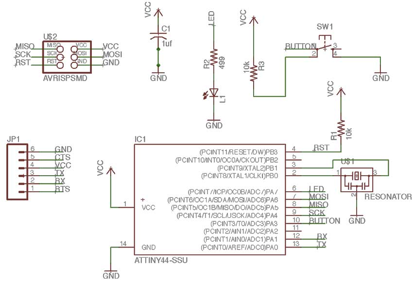
The first view is schematics. Here we are going to add
the components of the PCB, and connect them by "Net". In addition we
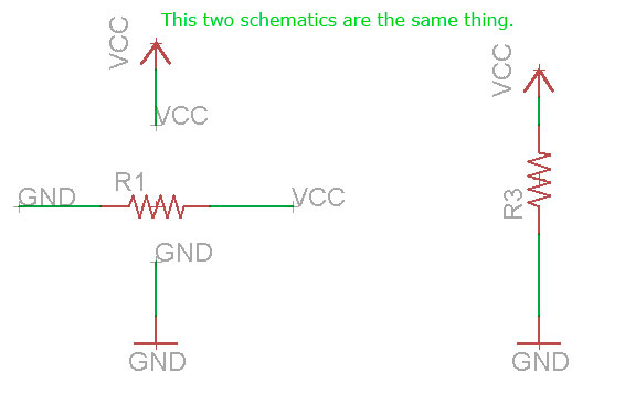
need two more components, also with the button add, VCC to give power
to the pcb and GND, to establish a ground en the pcb.
If we need to connect two components in a clear way, we could add
"labels" to connect nets or components which are not side to side.
Eagle will assume that all the labels that has the same name, are
connected. So if we put a NAME in a Label that are used in any other
part of the schematics, Eagle will ask us if we want to connect it with
the other label.
So, we add all the components of the pcb, and adding the two extra
components, the LED and the SWITCH:
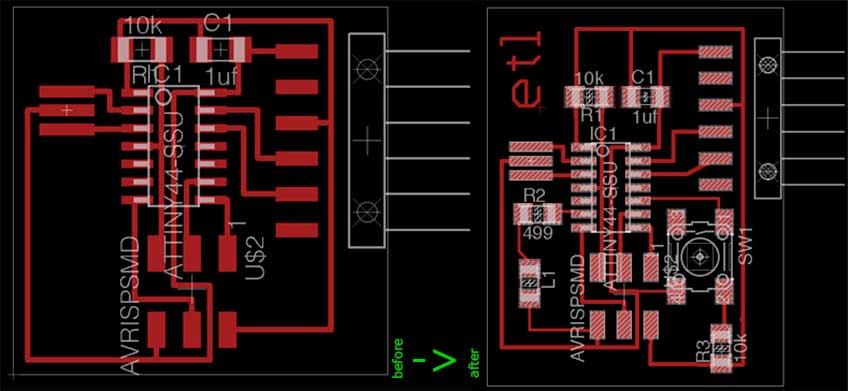
So now we have the schematics of the pcb, lets see if
Eagle could generate a optimized board that can have all the components
inside. So we press the button to switch between Shematics and Board (  ) , say YES to the question and
lets see what board Eagle draw. After this some components could be
outside the thin white rectangle (so, outside the board). This means
that we could position it where we want. Now the components has a
yellow line in their conexions , because we didnt simulate the paths
yet. ) , say YES to the question and
lets see what board Eagle draw. After this some components could be
outside the thin white rectangle (so, outside the board). This means
that we could position it where we want. Now the components has a
yellow line in their conexions , because we didnt simulate the paths
yet.
In the Free version of Eagle, all the components and
the limits of the board must be above and at the right of the white
cross. If not we are gonna have an error box.
Now, the first thing we are going to do is take all components and move
(right click -> move) inside the thin white line, that marks the
dimension of the board. If we need more space, we can move the vertex
of the white rectangle. At the finish we can make the board smaller,
but now we need some space :)
Once the components are inside, go to Tools ->
DRC... This are the Design Rule Check, where we stablish the needed
parameters to build the board. Open it and go to "clearance" tab. This
is the space between two copper lines. I put 16mil in all (we use a
1/64 mill ). Then we press "check" button and must say nothing (this is
good thing).
Now lets say Eagle we want him to do the hard job. Go to "Tools
-> Autoroute...". Then Eagle ask us how to do the autorute. I
selected the "1 Top" parameter with an * , and "16 bottom" parameter
with N/A. Press OK and watch the result....obviously this will be
wrong, its hard to do things at first attemp. So, we must
modify slightly the position of the components, to make easier the
Autoroute. Now repeat this until the result is right, and are not
yellow lines in the components.
To finish the job, we can use several tools, like
ripup, ratsnest or route. So here is the original board and my board:
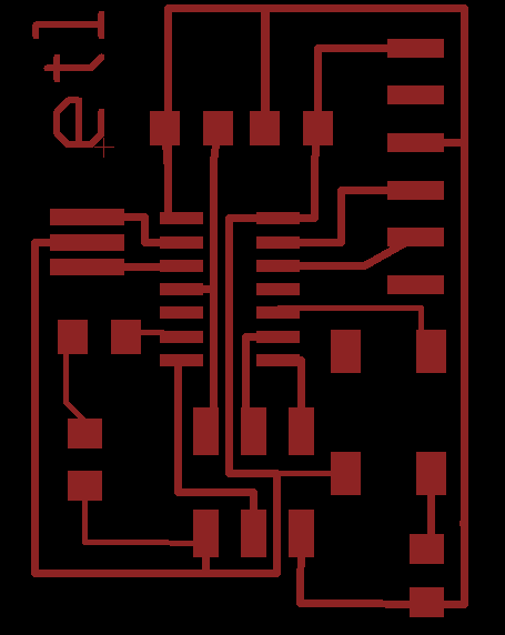
When we see that all components are inside the limits
and all the paths are correct, lets check if the board are
correct in electrical and design way. Now try to fix this errors...i
dont say this is going to be easy.
To the finish board i add a simple text. After add the
text, go to their properties and change the SIZE parameter to 0.15 or
above, and at the FONT parameter i choose "vector".
After all is finish, lets export the .png file to mill
it.
First of all lets hide all the layers, except the paths and pads. Go to
"View -> Layer settings..." and click in NONE.
Then click in layer number 1 and press OK.
You must have something like this: (maybe the black
region is greater than the design, but we will fix it later)
Then go to "File -> export -> image" and
select the name of the file, check the "MONOCROME" tip and the
parameter "RESOLUTION" must be at least at 500dpi.
Once you exported it, we need to add a frame around the image, of about
20 pixels. So open with your favorite photo editing tools (i use
photoshop) and the first thing you probably has to do is crop the image
and leave the definitive board size (like the imagen above).
Now we have the definitive size, lets make a little
edge. Make the canvas size 20 pixels greater in width and height, and
paint it in white.
If you make some modifications in the file, adding some
text or anything else to be drilled, remember to save the file in a
flattern image, i mean with just with ONE layer.
Finally we need two images, one with the inside paths and pads, and the
other with the edge of the board, like this:
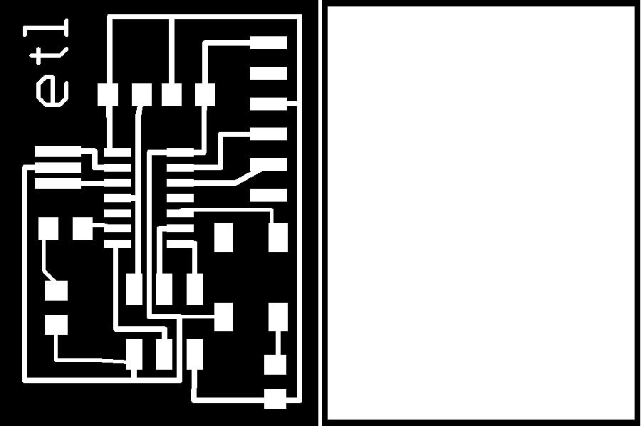
Click on the image to download the two files in PNG format.
REMEMBER:
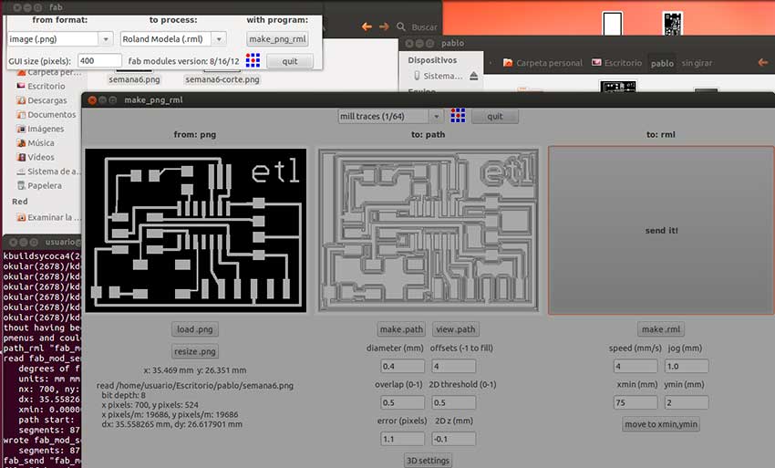
the Modela cuts the black parts and leave the white ones
After this we need to cut the piece in the Rolan modela machine, with the milling parameter that as good results we had.Open the fab modules and take all this parameter to mill the paths:(realize that i had to rotate the file 90º degrees because the copper plate has more space available in this orientation. PROBLEM:
when i turn the image in the default image visor of Ubuntu, it adds me
10 cm to all the magnitudes, and when i load in the fab modules says
that the pcb has 23cm wide, in spite of 2,3 cm. I recommend to turn the
file in photoshop or Gimp)
After
this step, the Modela has a problem with the board. It cuts good the
side more near than me and hardly can mill the part more away from me.This
is something that happens me before, so i do another pass but with the
parameter 2Dz in -0.2. Despite that the pcb doesnt seems to be milling
right, so the we reallize that the copper board wasnt well attached to
the bed of the modela. So after some pass more i had mi pcb really
really well cutted (it seems the Grand Canyon).
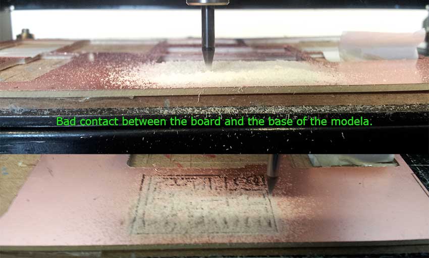
This
can help me to put the components much better than with a slightly
milled pcb. The solder dont try to touch another paths, it only goes
down in the inter-paths holes :).
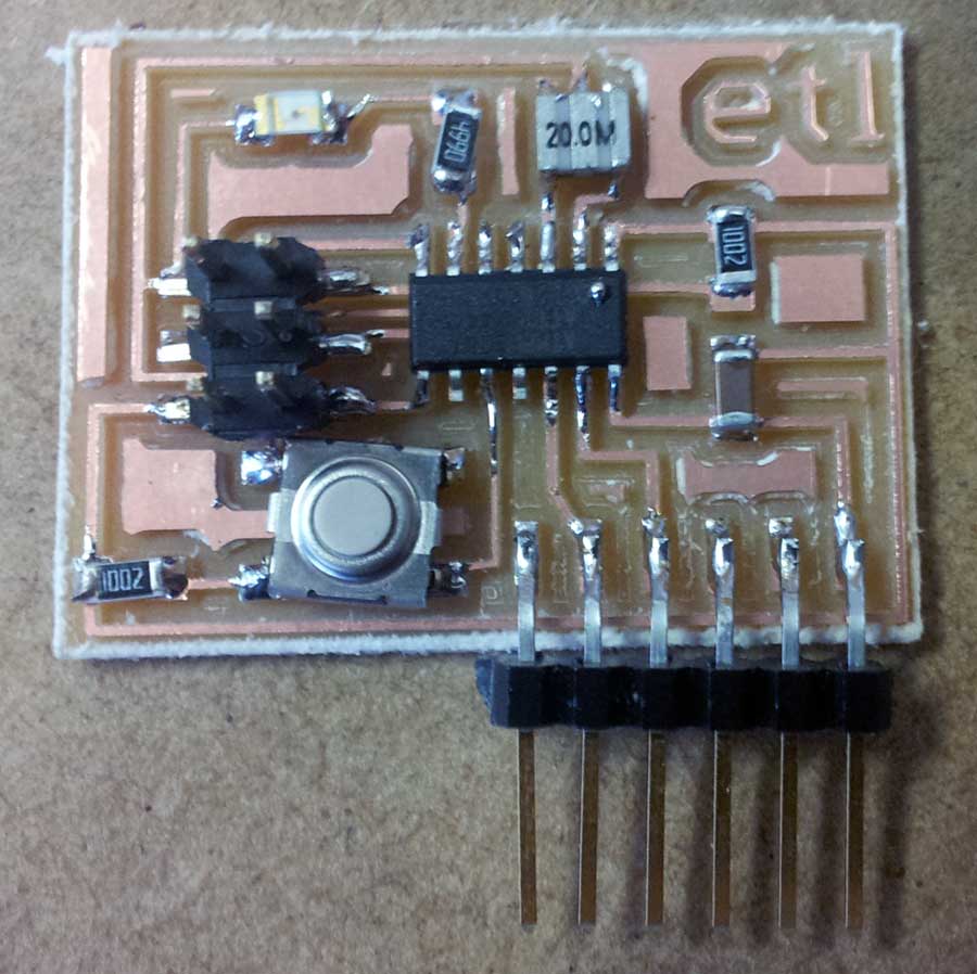
After this we need to collect the components and put in his right place:
RES-US1206 (RES-US): two of 10k and another of 499k
RESONATOR 20MhzA Led LED1206 (LED)A switch 6MM_SWITCH6MM_SWITCH (6MM_SWITCH)One ATTINY44-SSU (ATTINY44)One AVRISPSMD (AVRISP)
An FTDI-SMD-HEADERA CAP-US1206 (CAP-US) from 1uF
And put in the pcb with incredible mastery...oh ,well ,in my case enough good to make them stay at their positions. And finally this is the result:
|
