|
Week4: Electronics Production
This
week we learn the the different ways and materials to make a
PCB
with components inside. At the end of the week we must build the FabISP.
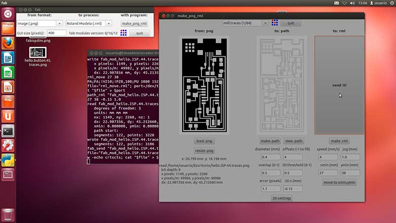
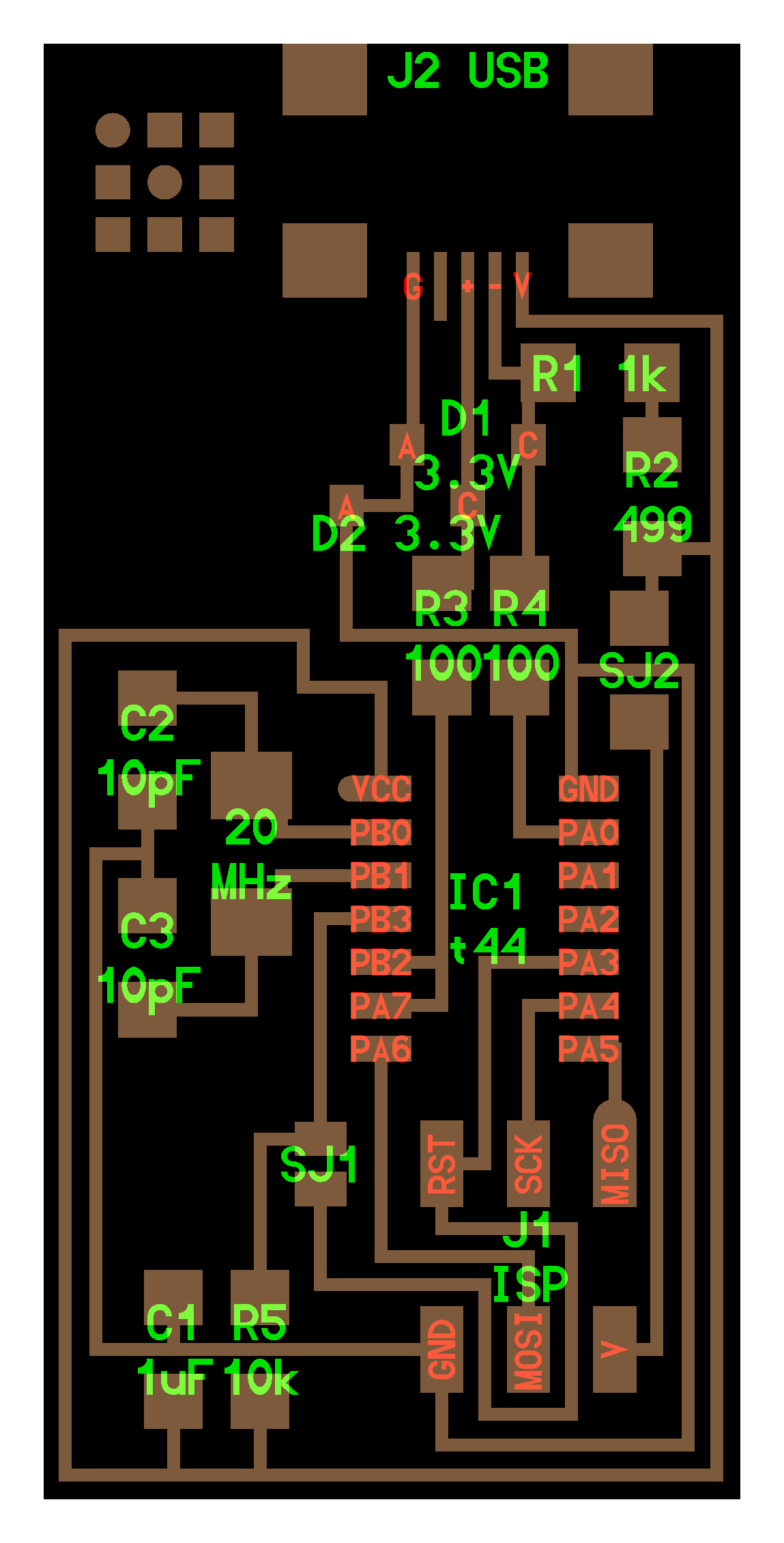
The
first thing we must do is to cut in a rigid PCB, with the Modela, the
diagram of the FabISP circuit. I choose the Hello.ISP.44.cad board,
because seems to be easier for my first PCB.I downloaded the traces file and the interior file from the Fab Academy web page.This
was my first time working with the Modela, and it seems to be a machine
with a lot of precision. Here in the Fab Lab Leon we had a great
workflow to work with the modela. The 1/64 endmill seems a really small
thing. First thing I need to do is practice with placing the Z axis in
the correct position. ¿Why this machine doesnt have a Z-cero caliber,
as the CNC? The way i must put the enmill touching the PCB is highly
stressful ! :)
After some testing finally
started to mill the PCB with the circuit. This was the parameters in
fab modules.
The
PCB seems not well attached to the base, so in half of the PCB the mill
do his job, but at the other half dont mill enough. To correct this i
made other pass , adjusting the Z a little bit down, as you can see in
the parameters. The first pass was with 2Dz at -0,1mm and the second
pass was with 2Dz at -0,15mm.
This seems to be enough to make a
nice cut with the 1/64 endmill.
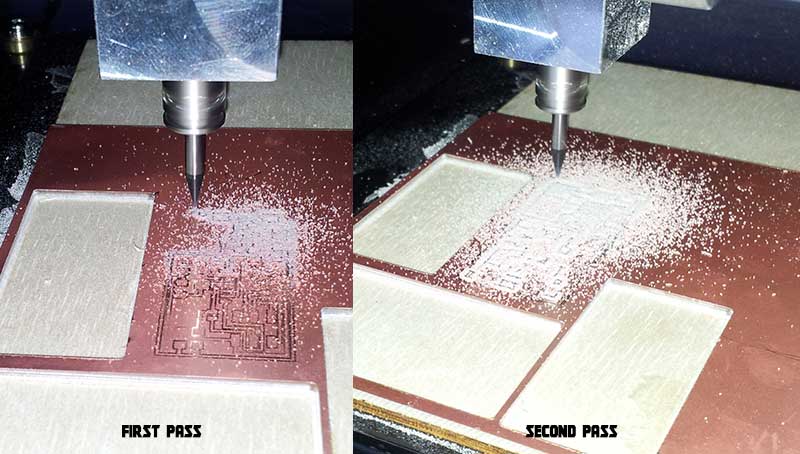
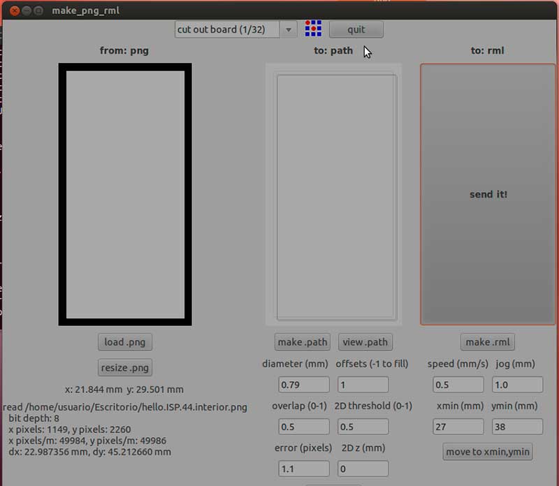
Finally I cut the margin with the
1/32 endmill with the following parameters:
Assembly components
Now we must fill the PCB with the
components required. This is the list and the diagram:
RESISTANCES: R1 1K // R2 499 // R3 100 // R4 100 // R5
10k
CAPACITORS: C1 1uF // C2 10pF // C3 10pF
DIODERS: D1 3,3v // D2 3,3v
An ATTINY 44 microcontroller
A 20Mhz Cristal
Mini USB conector
J1 ISP connector
Then
i solder the components on the PCB as seen on the diagram. Thanks to
Ruben Ferrero that teach me the basis of soldering with tin, my first
time soldering wasnt a nightmare. First i must heat the pad, then put a
little cuantity of tin, and then heat the pin of the component and the
pad at the same time. Finally we add a bit mor tin to cover the pin.
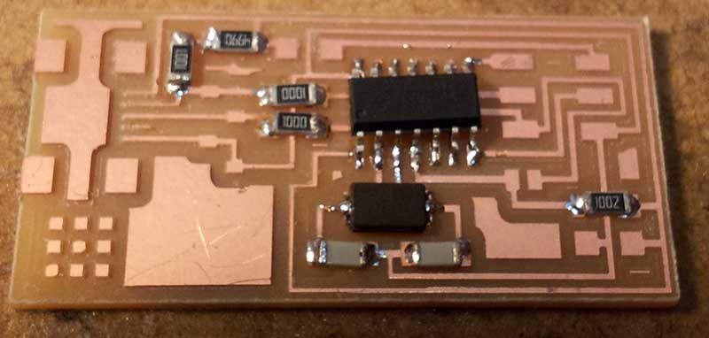
After
some practice, i get all the resistances, capacitors, dioders and the
ATTINY44 micro solder to the PCB. Then i must put the 0 resistances in
their position. A teammate in the fab lab, Alejandro, suggest me to put
a pair of jumpers in the 0 resistances position. So if in the
future if i need to reprogram the PCB, i just need to put the jumper.
If the software is ok ,i must remove the jumpers to avoid it to delete
the firmware.
So here are my tho jumpers in the PCB:
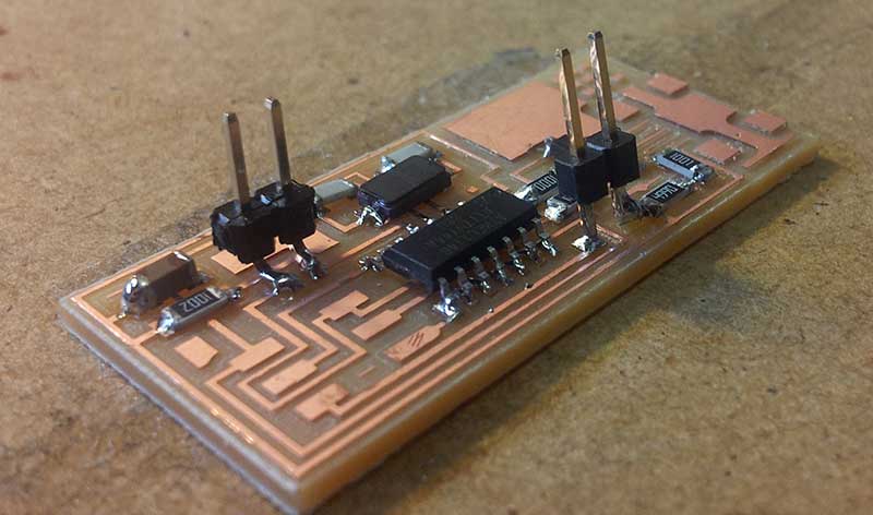
Yes, i know, i must improve my skills in soldering :)
Finally we add the J2 and J1 connectors and the Mini
USB.
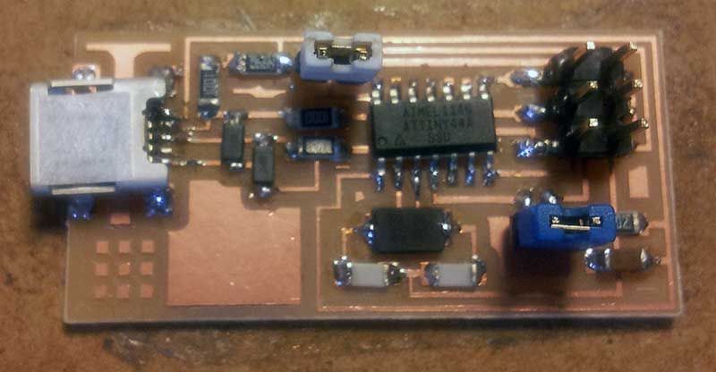
After
this, the multimeter says that some pins of the Mini USB arent well
solder. So i spend a hole morning trying to solve it. After check that
all the paths goes individually, i can finally program de FabISP.
Programming the FabISP
To
program it we use another valid FabISP in Fab Lab Leon. Connect the two
USB of the two PCB to a MAC computer, and then make a 6 pin cable to
attach at the J1 connector. Be sure the red cable are at the same
position in both PCB.
After this, make all the process:
nano Makefile (here we change the option to use MiniUSB
make clean
make hex
(sudo) make fuse (check programmer in Makefile, may need to repeat)
(sudo) make program
Everything
goes fine, and all the process completed with an OK. Then un plug the
PCB and try that a Windows computer recognice it as a FabISP....without
luck.
After spending couple of hours inspection it and
re-do all the process, my instructor Nuria Robles realized that the V
pin of the MiniUSB got out of the housing, and that was the problem.
So i must start all the process again, to get a shiny
new FabISP Programmer.
! electronic are really hard job !
UPDATE:
finally i review all the pcb and find some traces that arent well
connected, and at the end i could program the FabISP and it can program
other boards....!great!Starting with the Andy FABIsp
After
realize that the mini USB connector is a nightmare to a new-born in
soldering like me, i try the Andy FabISP, which has a built in USB
connector in his copper layer. So no more small pads to solder the
miniUSB... yahooo!!!
I
download the routes and the interior, milled in the Roland modela and
solder the components on it. The schema isnt really self-explaining,
because the ground are all around the programmer, so its hard to see
clear which pads are for which component.
After guess the components i solder all the stuff in the pcb, and got a FabISP.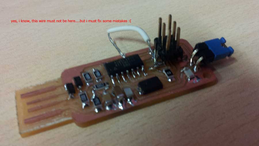
Unfortunately
this fabISP isnt working no more. My skill in solder wasnt good enogh
for this programmer, and i finish burning the traces.Later in time i try to fix this board, and finally got a FabISP with USB incorporated...nice and small.
If you cant build a FabISP and has an AVR programmer, you can use it to program the nex boards in the Fab Academy.
Installing the programmer AVR in Windows 7 64 bits:
|
