Week 8 – Electronic Production
Fab Academy – Week 8
Date range: 11 - 17 Mar
Instructor: Neil
🧠 Learning Objectives
- Describe the process of tool-path generation, milling/laser engraving, stuffing, de-bugging and programming
- Demonstrate correct workflows and identify areas for improvement if required
📋 Assignments
Individual Assignment
- Make and test a microcontroller development board that you designed
Group Assignment
- Describe the process of tool-path generation, milling/laser engraving, stuffing, de-bugging and programming
- Demonstrate correct workflows and identify areas for improvement if required
🛠️ Tools & Materials
- Software (KiCAD, Fusion 360, Bambu Studio, )
- Machines (PCB, BambuLab A1)
- Materials (PLA, Copper Foil tape, PCB board, and electronic components)
👥 Group Assignment
🧪 Process & Workflow
Step 1 – Design
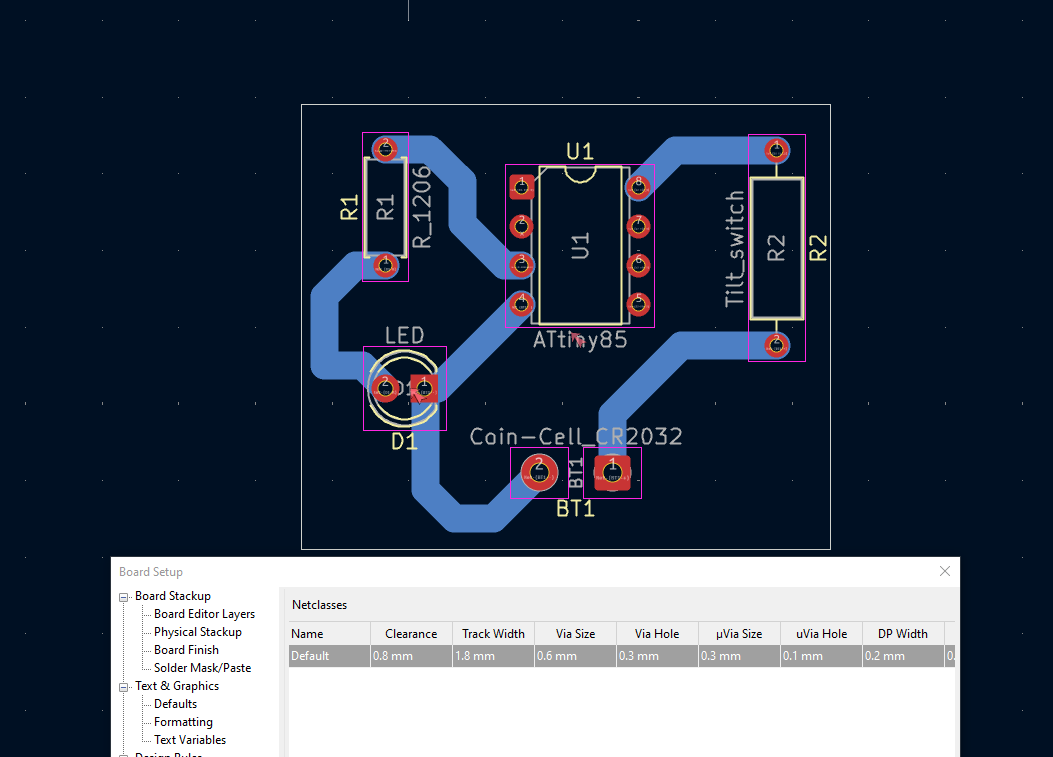
After checking the design rules for the machine I’m using, I updated the track width and clearance for the PCB design. Track width is 0.4mm and Clearance is 0.2mm.
Went to File>Fabrication Outputs to generate the Grbers files. Choose the layers you need, in my case it was just the F.Cu and Edge.Cuts. Press Plot, the Generate Drill files.
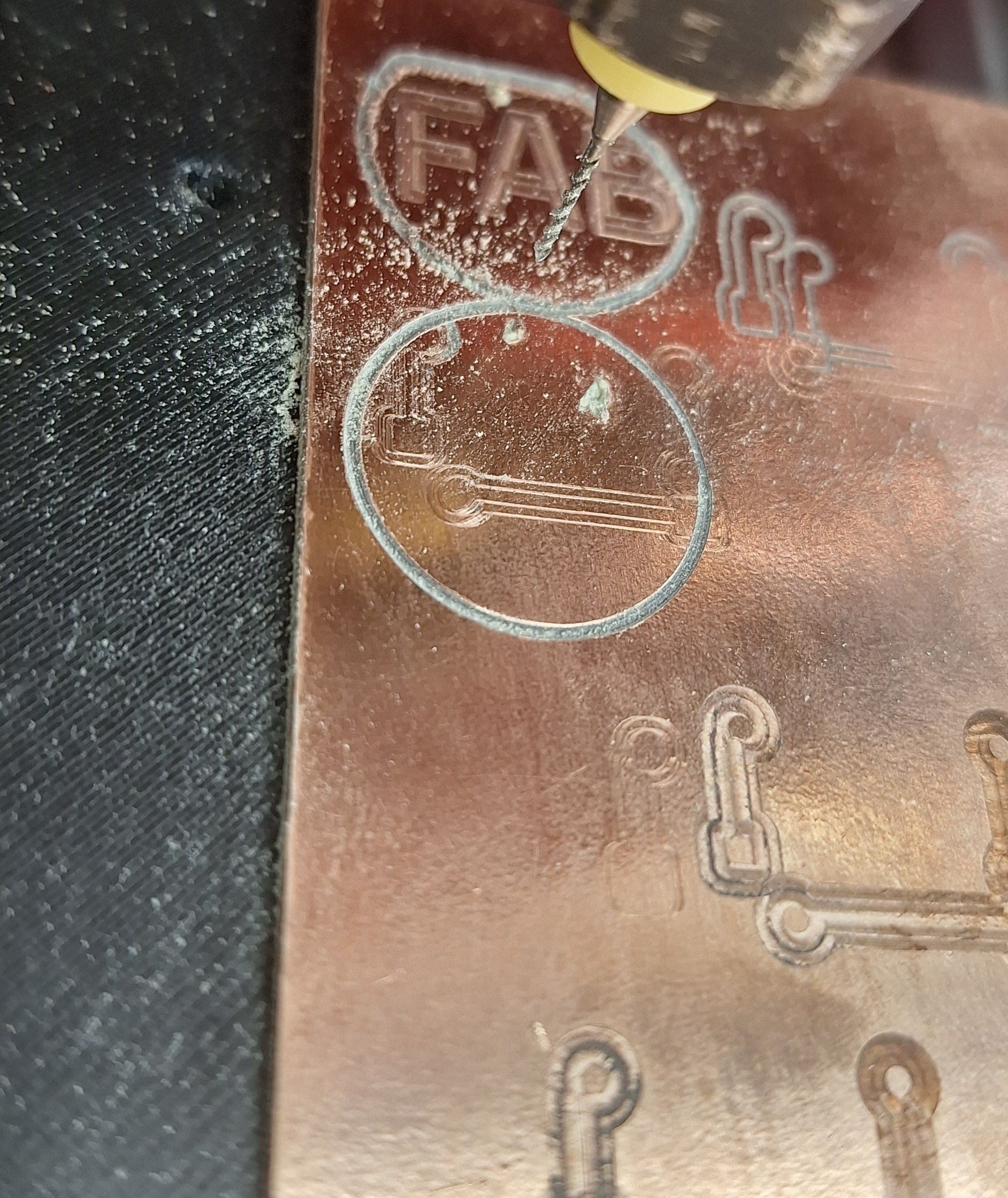
Step 2 – Fabrication
For milling for I need to document: feeds, speeds, plunge rate, depth of cut (traces and outline) and tooling.
I tested a different speeds and feed for the machine I’m using and the endmill. I found the following parameters generate good result.
| Feed rate x-y | 100 |
|---|---|
| Feed rate z | 60 |
| Spindle Speed | 10000 rpm |
| Depth each pass | 0.1mm |
| Endmill bit | 0.4mm fluted |
I still need to finish this part, as I realized I made a mistake in my cirucut where in KiCAD I'll update and document.
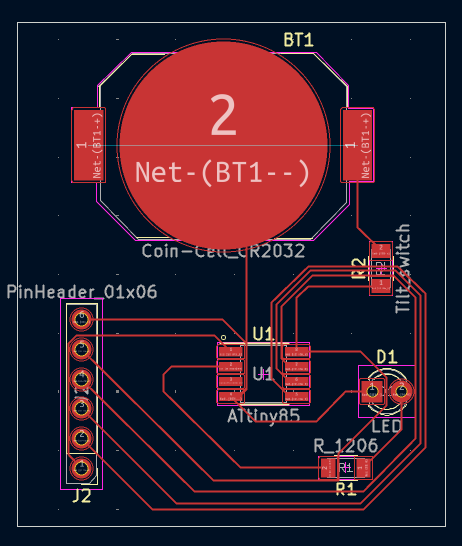
Here I modified my circit design and milled it:
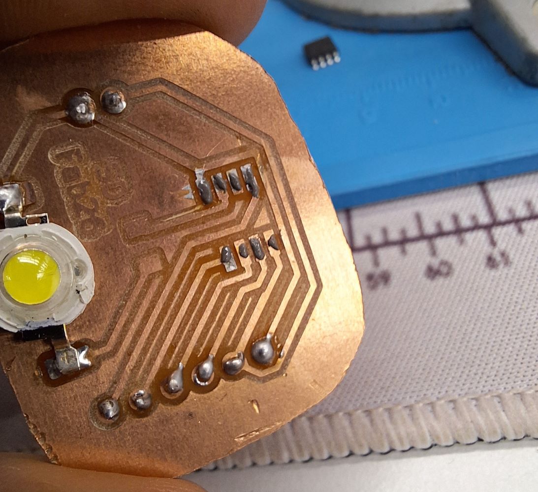
Step 3 – Soldering
For the tiny ATtiny85 I used the soldering paste and then a heat gun:
🧪 Alternative Workflow
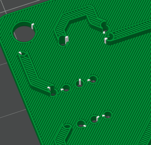
I wanted to try using the 3D printer for making PCBs. I found an interesting method here, and I wanted to test and document.
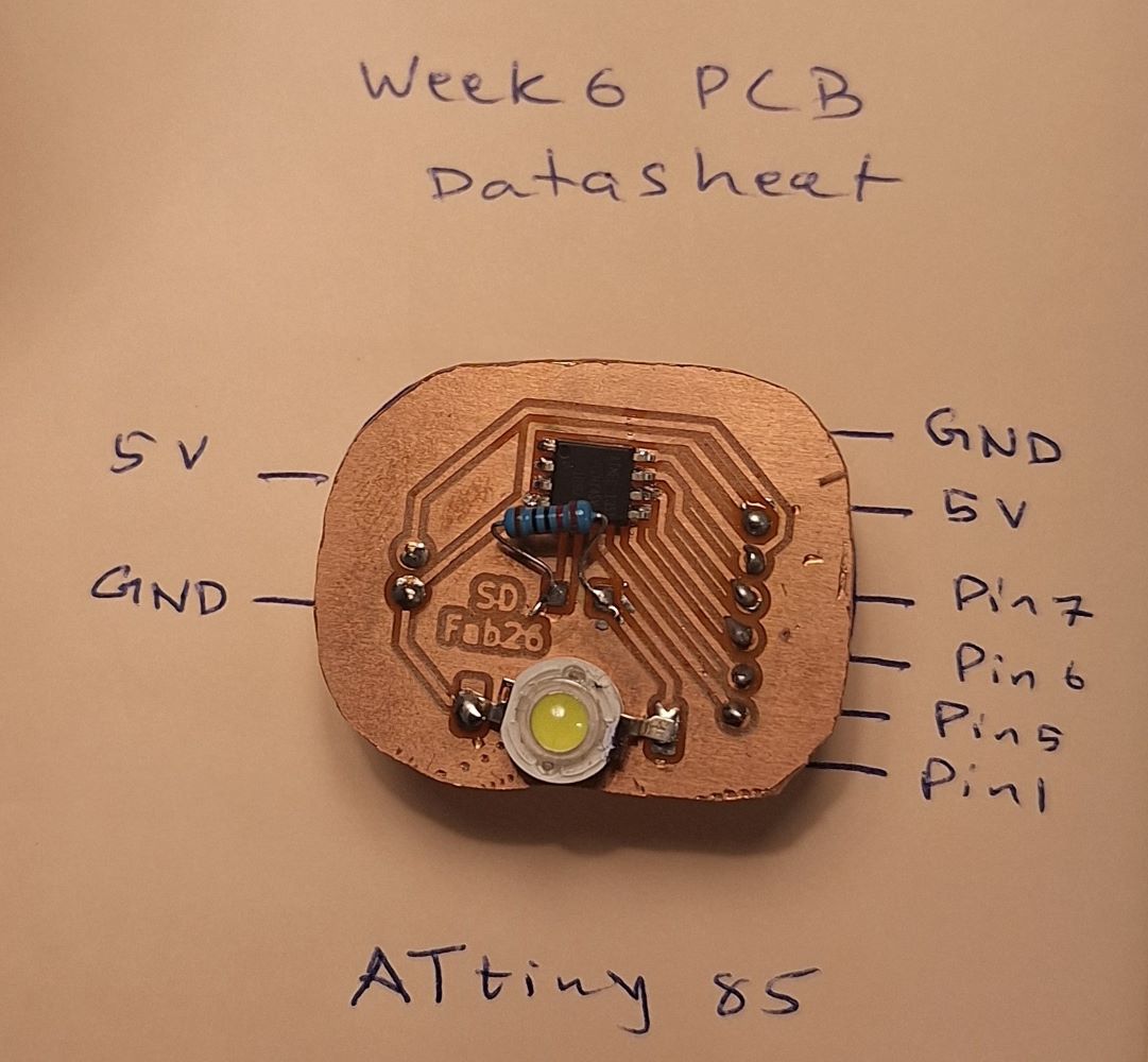
I went back to my circuit from week 6 I remove the pin headers for programming to make it simpler.
For this I did the routing on the B.Cu layer, which does the routing on the back of the board. Then in the Board setup under Design Rules > Net Classes I played with the track width and clearance without any rout conflicts, trying to make track width minimum 1.8mm and clearance 0.9mm, if your board allows for larger numbers, increase them.
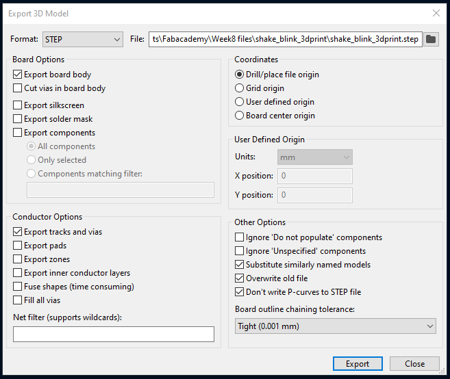
Next, I need to export this design to a format suitable for fusion360.
File>Export>STEP make the following selections and select export directory then press Export.
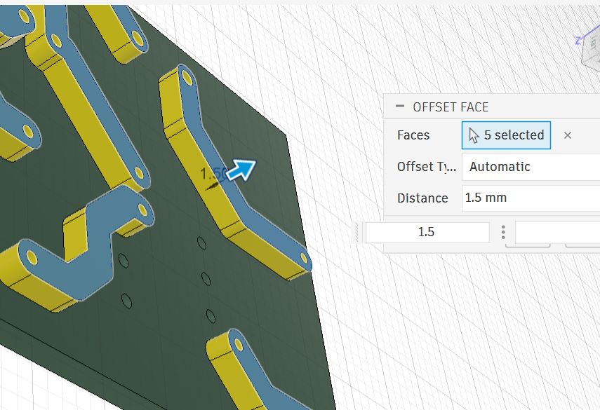
Open the STEP file in fusion and extrude the tracks, making sure it doesn’t exceed the length of the pins of your components as we want them to stick out. In my case the ATtiny85 has the shortest legs, which is 4mm. The board in the step file by default is 1.51mm so I pulled the tracks another 1.5mm.
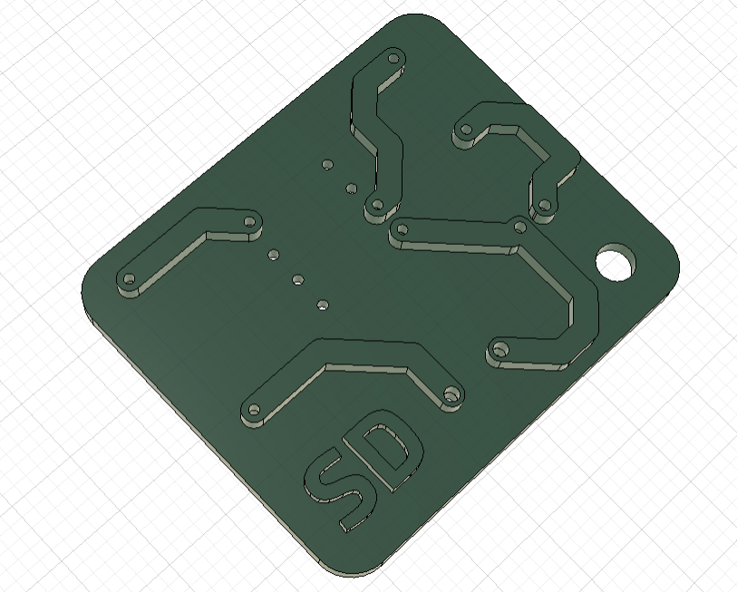
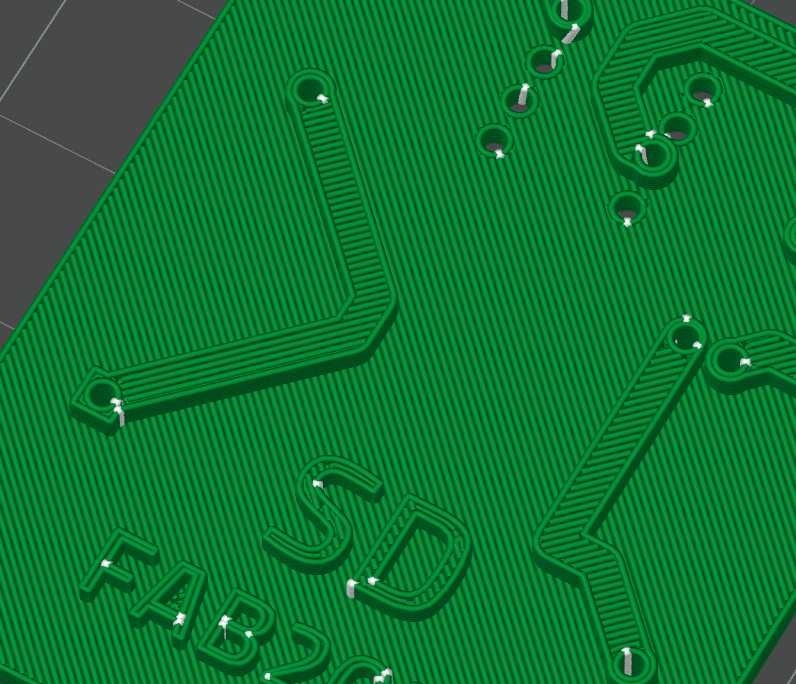
I rounded the edges, added a hole for a keychain, combined the bodies and added my initials.
I printed the first version and it was too small, a PCB for ants. I adjusted the size of the battery holder and the holes diameter.
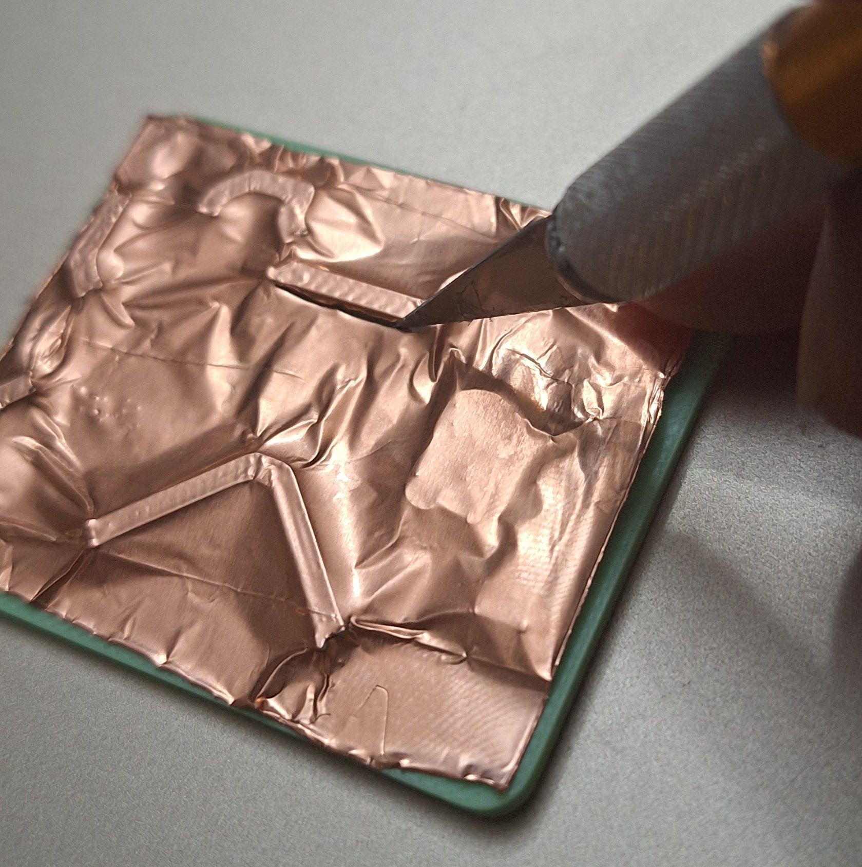
After printing, I applied a copper foil tape on top and traced with an exacto knife to remove the excess and keep only copper foils on the tracks.
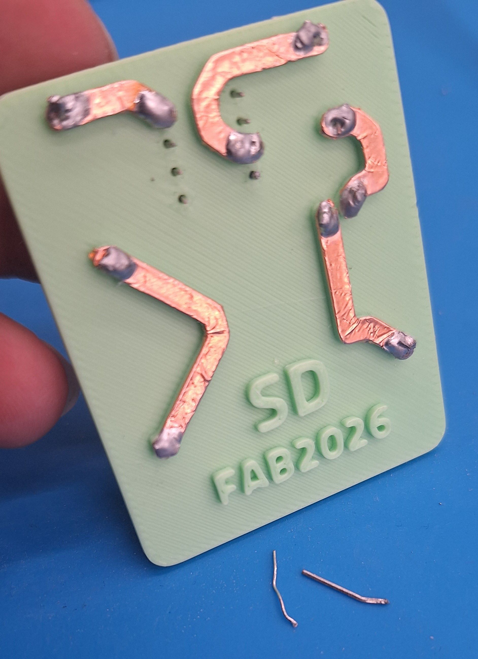
Final step was to solder. For the battery holder, I had to improvise as the one I had was for sewing circuits, so I glued the battery holder to keep it in place then soldered. I forgot to take a picture for this step. But I basically used the pins I cut from the resistor and attached them to the battery, then put them trough the holes and soldered them on the opposite side.
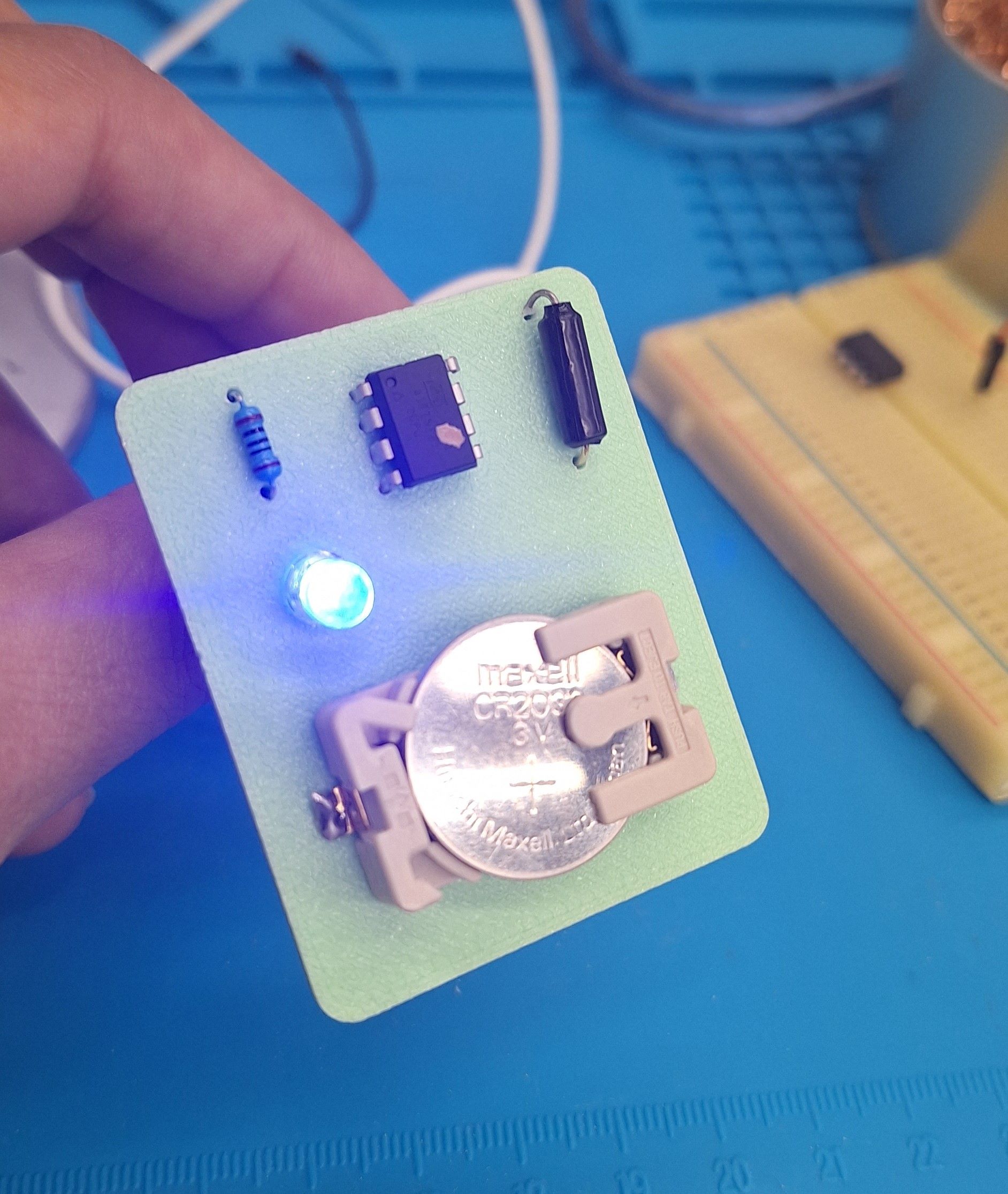
Final result, and moment of truth.
Next, I will try to seal the circuit in a way to protect it.
🔍 Electrical Testing, Verification & Troubleshooting
1. Continuity & Power Verification (Pre-Power Checks)
Before connecting the board to a power source, a multimeter was used in Continuity Mode (with a BEEP icon) to verify the structural integrity of the traces:
-
Ground-to-VCC Isolation: Placed probes on the
5VandGNDlines to guarantee there was no direct short circuit. The multimeter remained silent (Open Circuit), confirming it was safe to power. -
Trace Continuity: Verified continuity from the microcontroller pins directly to the header pins to ensure clean solder joints and no hairline cracks in the milled copper traces.
2. Debugging & Troubleshooting Process
During initial testing, the board experienced an intermittent power failure where the status LED would flicker and the computer would lose connection to the serial port.
-
The Problem: A visual inspection under a magnifying glass revealed a cold solder joint on one of the pads of the microcontroller. The connection was making contact only under physical pressure. Furtnately this pin was only needed during programming, so I placed a small copper wire temporarily until I finish programming.
-
The Permenant Fix: I reapplied a small amount of flux, used a soldering iron to reflow the joint cleanly until the solder flowed smoothly onto the pad, and re-tested. The connection stabilized immediately.
⚠️ Problems & Solutions
- The track width for the 3D printed circuit board was still not enough for 3D printing in relation to the hole diameter. I will try to play around in KiCAD to find a more appropriate settings.
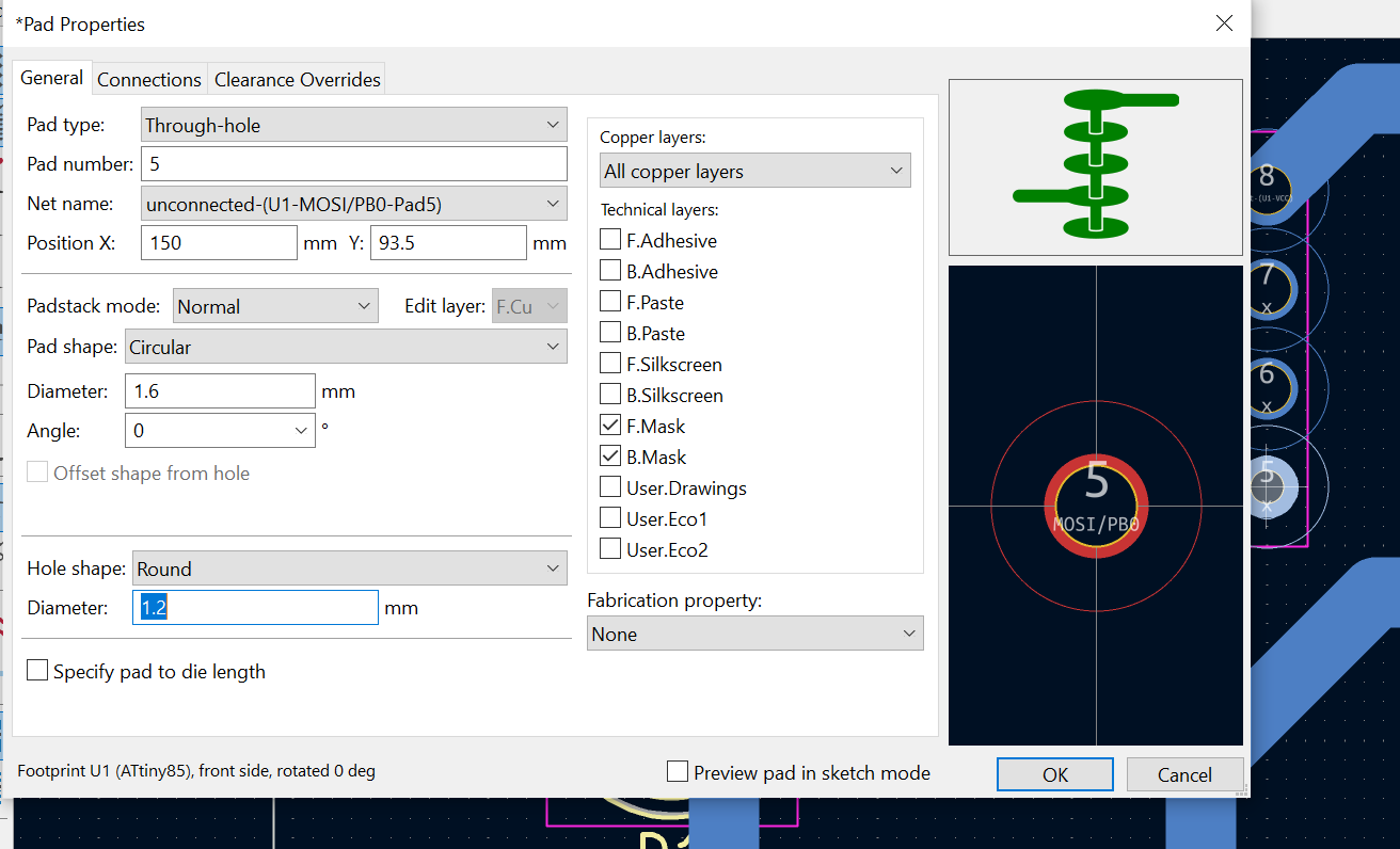
- I played a bit in KiCAD with the hole diameter, track width and pad sizes until it was fixed
The parameters I used:
| Track width | 2.4 |
|---|---|
| Hole Diameter | 1.2 |
| Pad Diameter | 2.6 |
🧩 Files
📝 Reflection
- PCB design and production was a new and exciting learning curve for me. I started at not knowing what am I doing, to understanding the workflow and being able to test multiple alternatives, I will for sure continue making more PCBs even after finishing fab academy.