Week 6 – Electronic Design
Fab Academy – Week 6
Date range: 25 Feb- 3 Mar
Instructor: Neil Gershenfeld
🧠 Learning Objectives
- Select and use software for circuit board design
- Demonstrate workflows used in circuit board design
📋 Assignments
Individual Assignment
- Use an EDA tool to design a development board that uses parts from the inventory to interact and communicate with an embedded microcontroller
Group Assignment
- Use the test equipment in your lab to observe the operation of a microcontroller circuit board (as a minimum, you should demonstrate the use of a logic analyzer)
- Document your work on the group work page and reflect what you learned on your individual page
🛠️ Tools & Materials
- Software (KiCAD, Fusion360, Wokwi)
- Machines (BambuLab A1, generic multimeter)
👥 Group Assignment
For this group assignment we explored a few lab tools for debugging and measuring electronics: the Multimeter, the Oscilloscope, Power Supply and Signal Visualization.
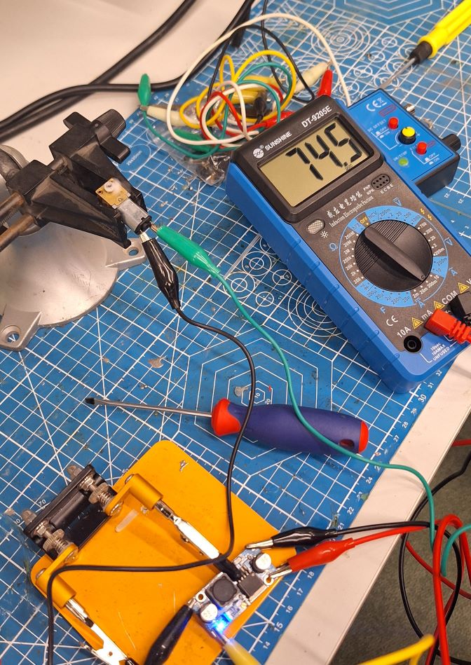
Multimeter: The Static Check
We began by using a digital multimeter to verify the basics of the circuit.
- Continuity: We tested the connections between between different jumper wires and power supply.
- Voltage: We measured the 5V and 3.3V output pins of the Arduino to confirm the power supply was stable and accurate.
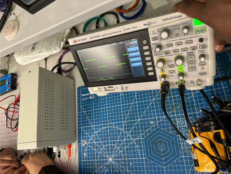
2. Oscilloscope: Seeing the Signal
To observe the "invisible" behavior of electricity, we used a digital oscilloscope. We wanted to see how the Arduino actually controls the power using Pulse Width Modulation (PWM).
- The Setup: We connected the oscilloscope probe to the PWM pin (Pin 9) running the "Fade" example code.
- Observation: Unlike a multimeter which shows a steady average voltage, the oscilloscope revealed a wave.
analogWrite(): We discussed how this function doesn't actually output an analog voltage, but rather a digital signal switching very fast (approx. 490Hz or 980Hz depending on the pin).
🧪 Process & Workflow (Individual Assignment)
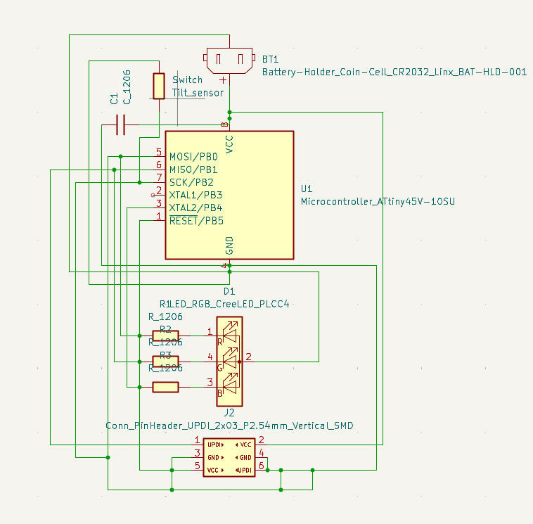
For this assignment I chose a fun small project using an ATtiny85, an LED and a pin headers for power and programming.
Step 1 – Wokwi Simulation Setup
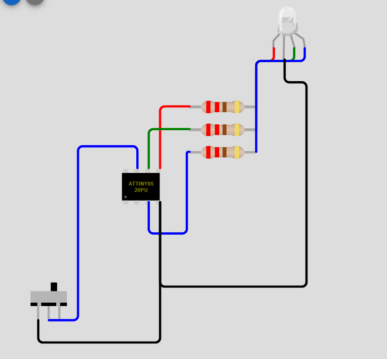
First step is to prototype it on wokwi and test the logic for a simple blink code. So I started a new Wokwi ATtiny85 project, the added the required components.
- Pin 2 (PB2/Tilt): Connect to theTilt Sensor (in wokwi I added a simple switch).
- Pin 4 (GND): Battery (-) and LED Long Pin.
- Pin 5 (PB0/Red): Through a resistor to the Red leg.
- Pin 6 (PB1/Green): Through a resistor to the Green leg.
- Pin 7 (PB4/Blue): Through a resistor to the Blue leg.
- Pin 8 (VCC): Battery (+) not simulated on wokwi.
Step 2 – Circuit Design
Installing KiCad then following the steps here, to add fab academy’s electronic library.
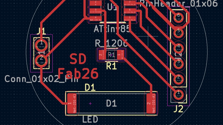
Schematic Design
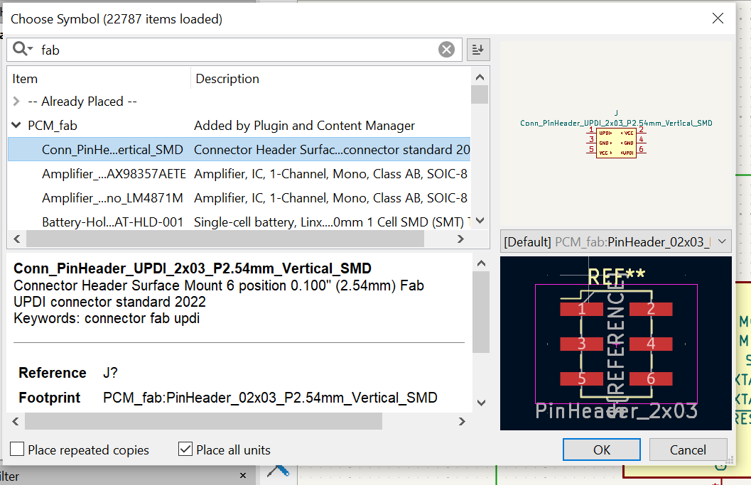
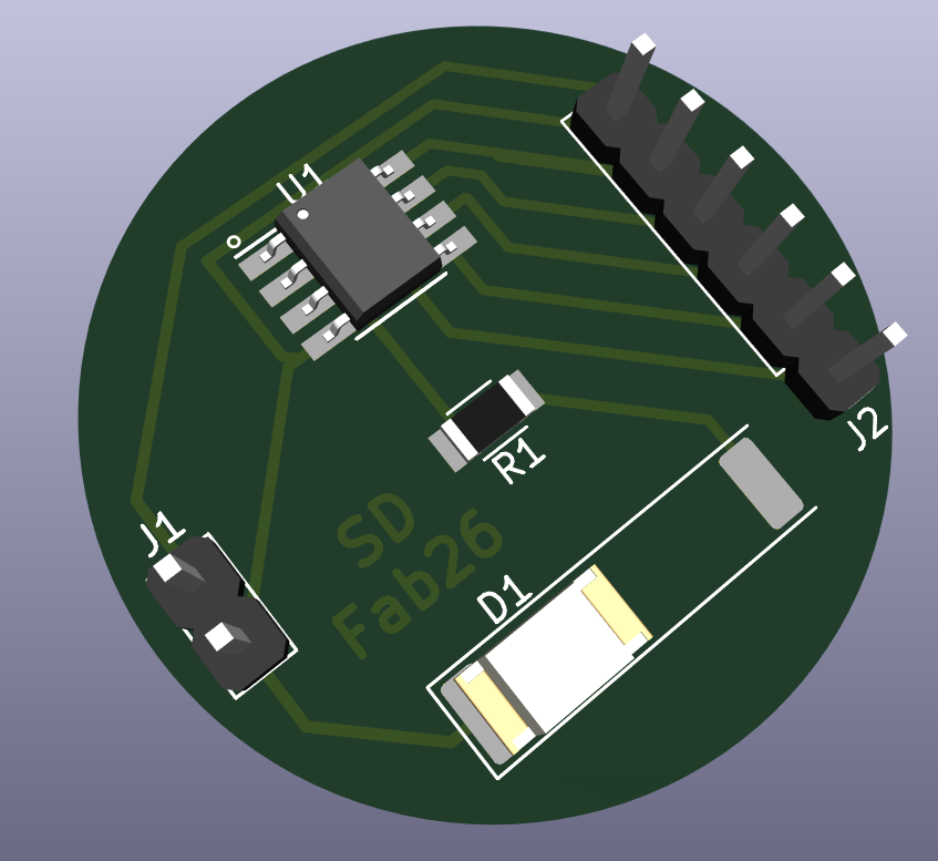
The logic was built around the ATtiny85 microcontroller. To ensure the board is programmable in the lab, I integrated a standard 1x06 Pin Header, I plan to program it with an Arduino Uno as a programmer.
- Key Components: SMD ATtiny85, a SMD LED, 1206 resistor, and Pin headers.
I started by placing the components in for the schematic, press A to load up the library and choose a component to place.
- Safety Check: Performed an Electrical Rules Check (ERC) to ensure no pins were floating and all power nets were properly terminated.
The check returned with two errors, one for the power not provided, and it was fixed by placing a power flag on the power pins, and one was about pin2 not being connected to anything, which was fixed by placing No Connect flag on the pin to indicate it was left intentionally.
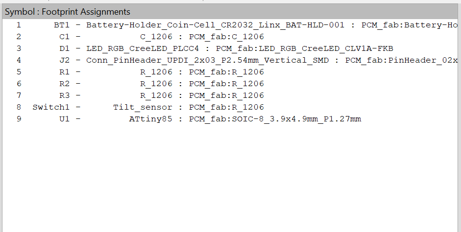
After finishing the schematic, I did a check on the assigned footprint to make sure that I have the right components that are maching what I actually going to use.
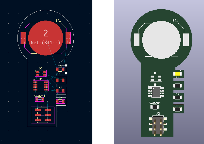
Physical Layout & Aesthetics
I started the PCB editor with “Switch to PCB Editor” from the tools menu.
- I arranged the components in a way that makes it easy to handle and route, hover over a component the press M on the keyboard to move and R to rotate.
Routing & Design Rules
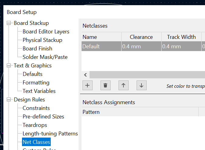
Since this board will be milled, I had to set specific design constraints to ensure the traces wouldn't be damaged during the milling process.
- From Board setup under file menu, choose Design Rules: Set Track Width and Clearance to 0.4mm to accommodate the size of the milling bit.
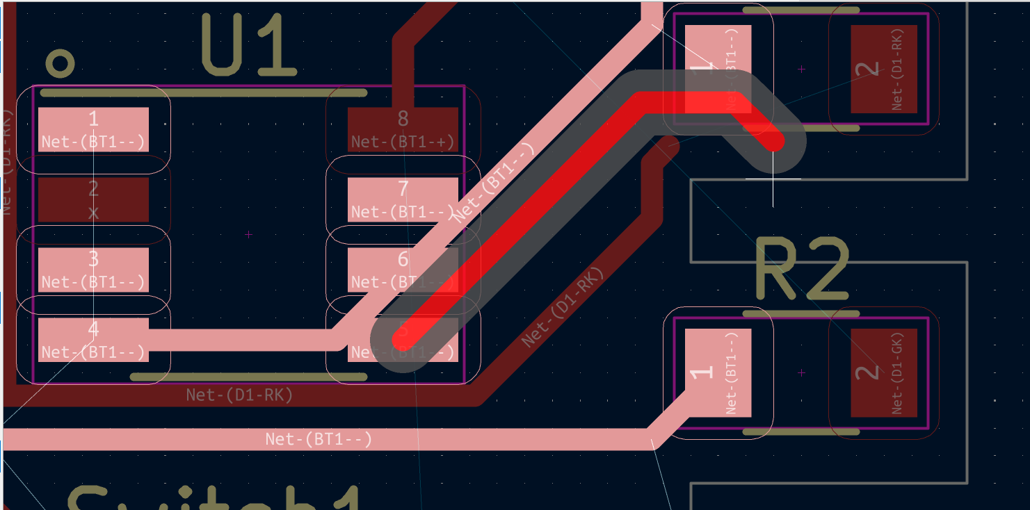
- Routing: it requires a lot of thought on how to rout the connections as the will overlap and you’ll have to re-arrange the components.
Running into issues wiring the PCB.
Final Routing after fixing
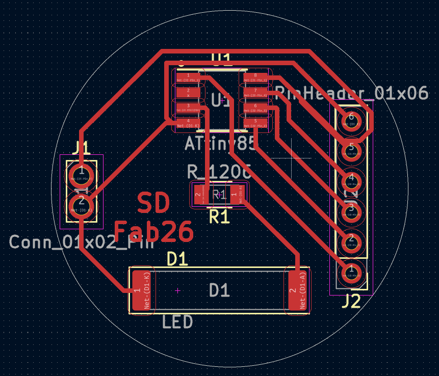
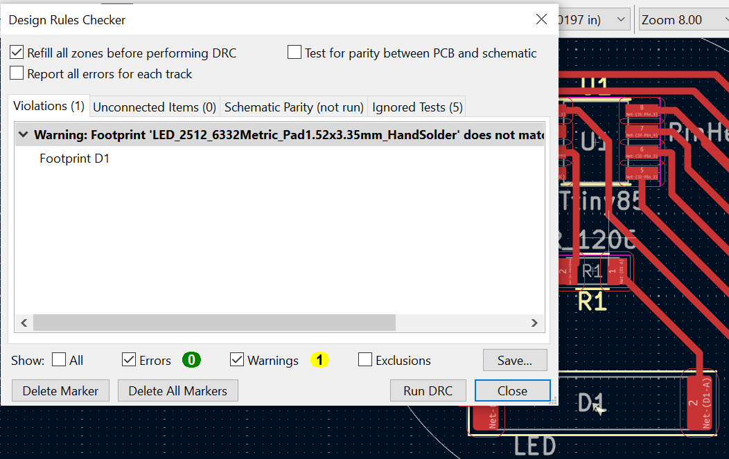
- DRC: running a Design Rules Check after finishing the routing to make sure nothing violates the design rules. The DRC returned an error regarding the LED because I had to modify the component's size to match the one I have, which I couldn't find in the library, but I manually verfied the clearance for the LED to ensure the mill bit can still pass between the pads.
 And here's a 3D view, apart from the LED, it looks good:
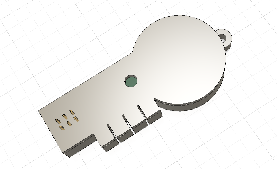
3D Design
The final step was modelling a 3D case for the PCB. KiCAD generated the 3D file which I was able to import into Fusion 360. In this workflow I used another PCB design that I worked on before.
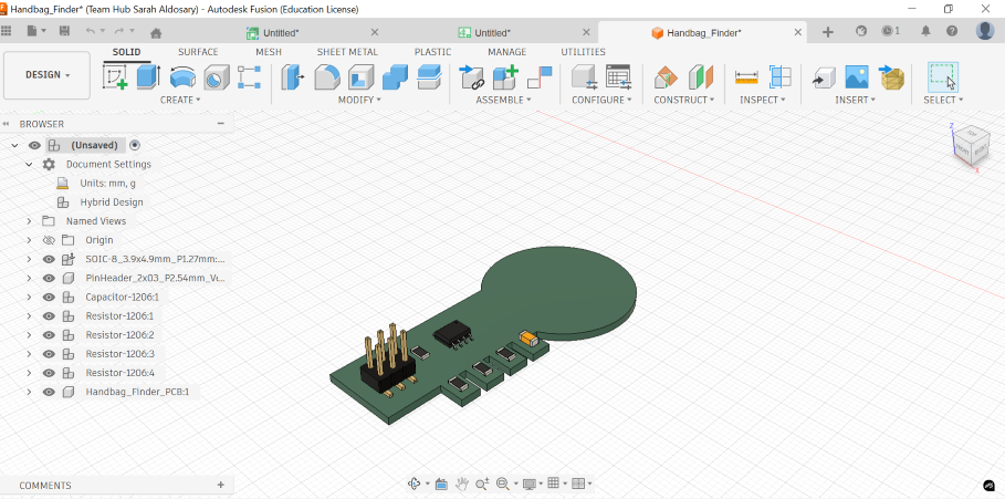
Here’s a rough design for the final part
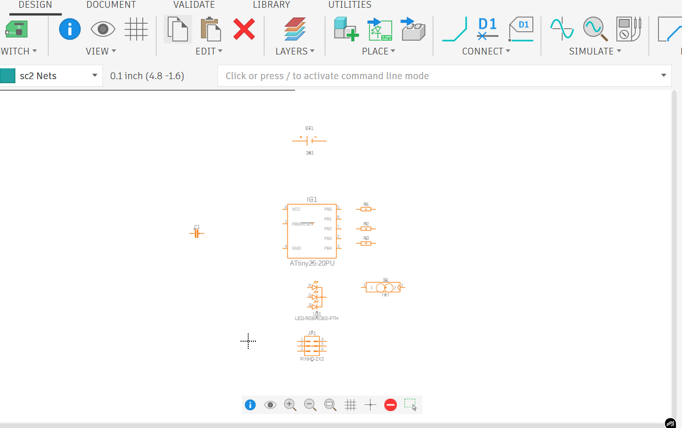
Step 3 – Testing another workflow - Fusion360 Electronic Design
The steps are almost the same as KiCAD, I started inserting the required components.
⚠️ Problems & Solutions
- Routing the PCB wires is a headache, I still haven’t figured it out. I will try to do it on wokwi then translate it on the PCB editor.
🧩 Files
📝 Reflection
- I realized that starting with a 3D model is a good way to get a feel of how the electronics can go. Since it’s my first time designing a PCB, I wasn’t sure how big or small it will be or could be, until I imported it in Fusion360 I realized I have more room for spacing the components, which is what I will be doing next.