Week 06: Electronics Design
Overview
This week's assignment focused on learning the complete PCB design workflow using an Electronic Design Automation (EDA) tool.
For this assignment, I designed a custom breakout board based on the Seeed XIAO RP2040 using EasyEDA Standard Edition. The board includes GPIO breakout headers, an onboard LED, a push button and an LDR input.
Installing EasyEDA
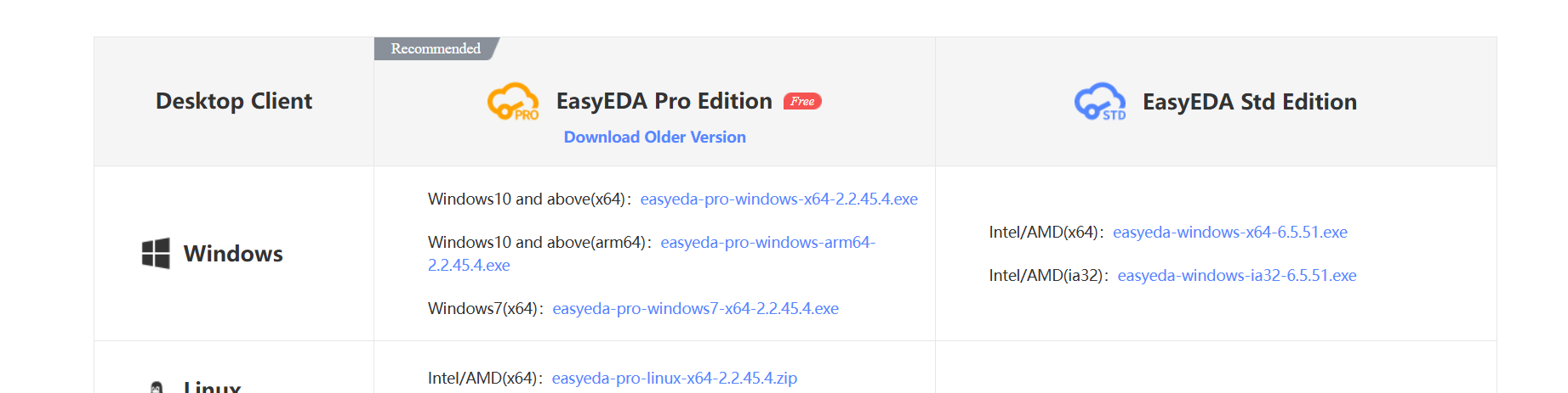
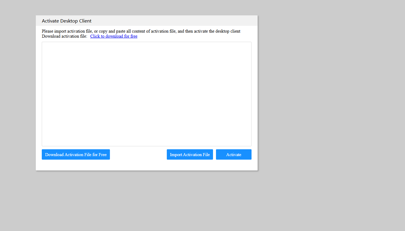
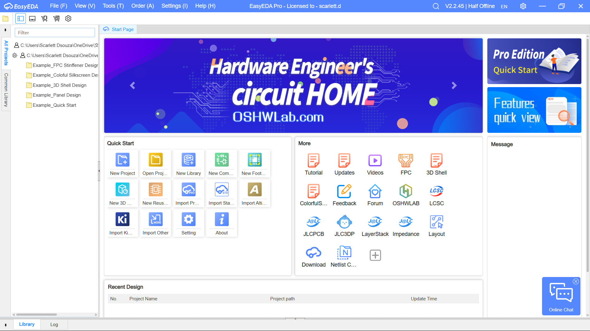
I initially downloaded EasyEDA Pro Edition, expecting to use it for the assignment. However, after installation I discovered that the software required an activation file before it could be used.
Since the Standard Edition already contained all the tools required for schematic capture and PCB design, I switched to EasyEDA Standard Edition and continued the project there.
Creating a New Project
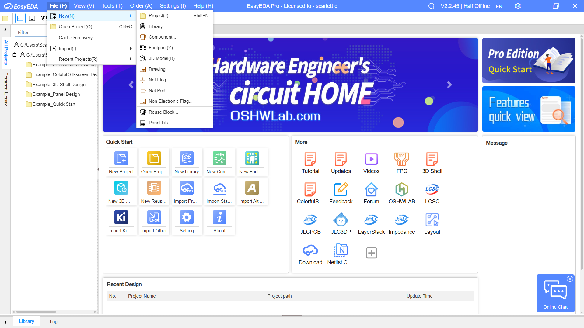
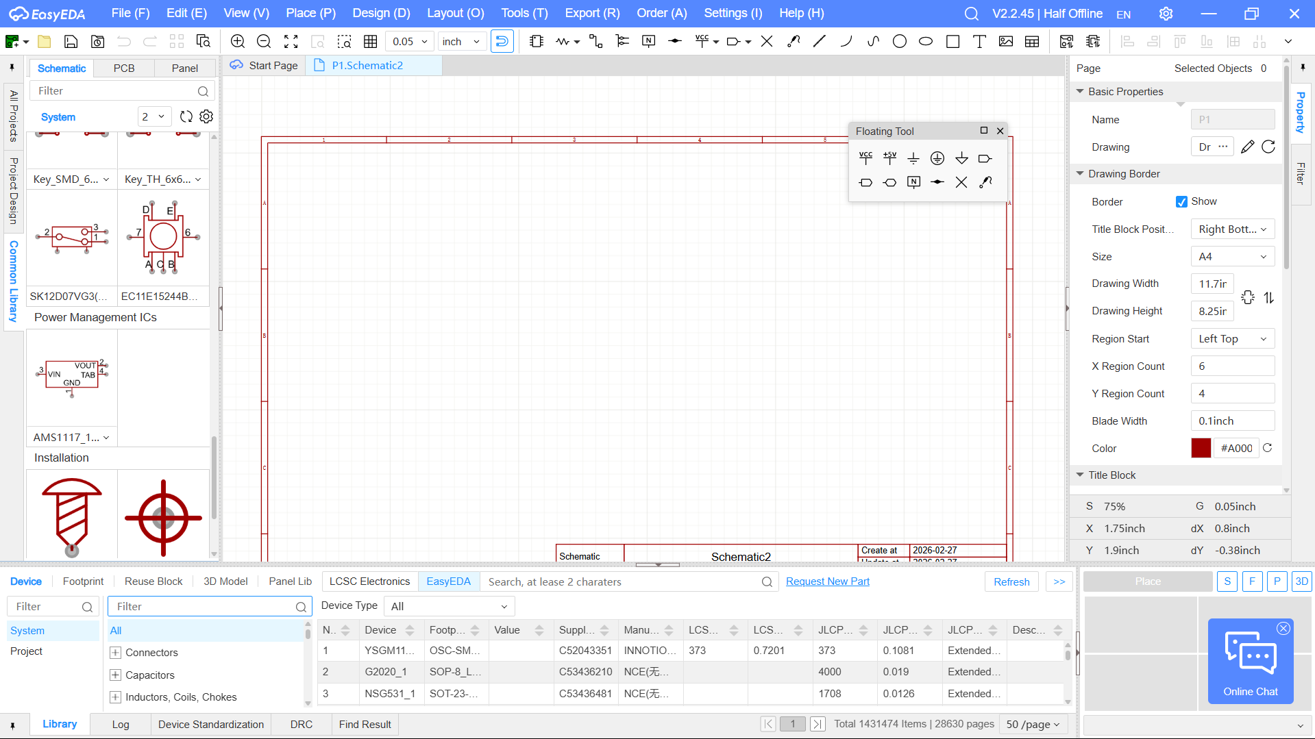
After installing EasyEDA Standard, I created a new project and opened a blank schematic workspace where I could begin building the circuit from scratch.
Selecting Components
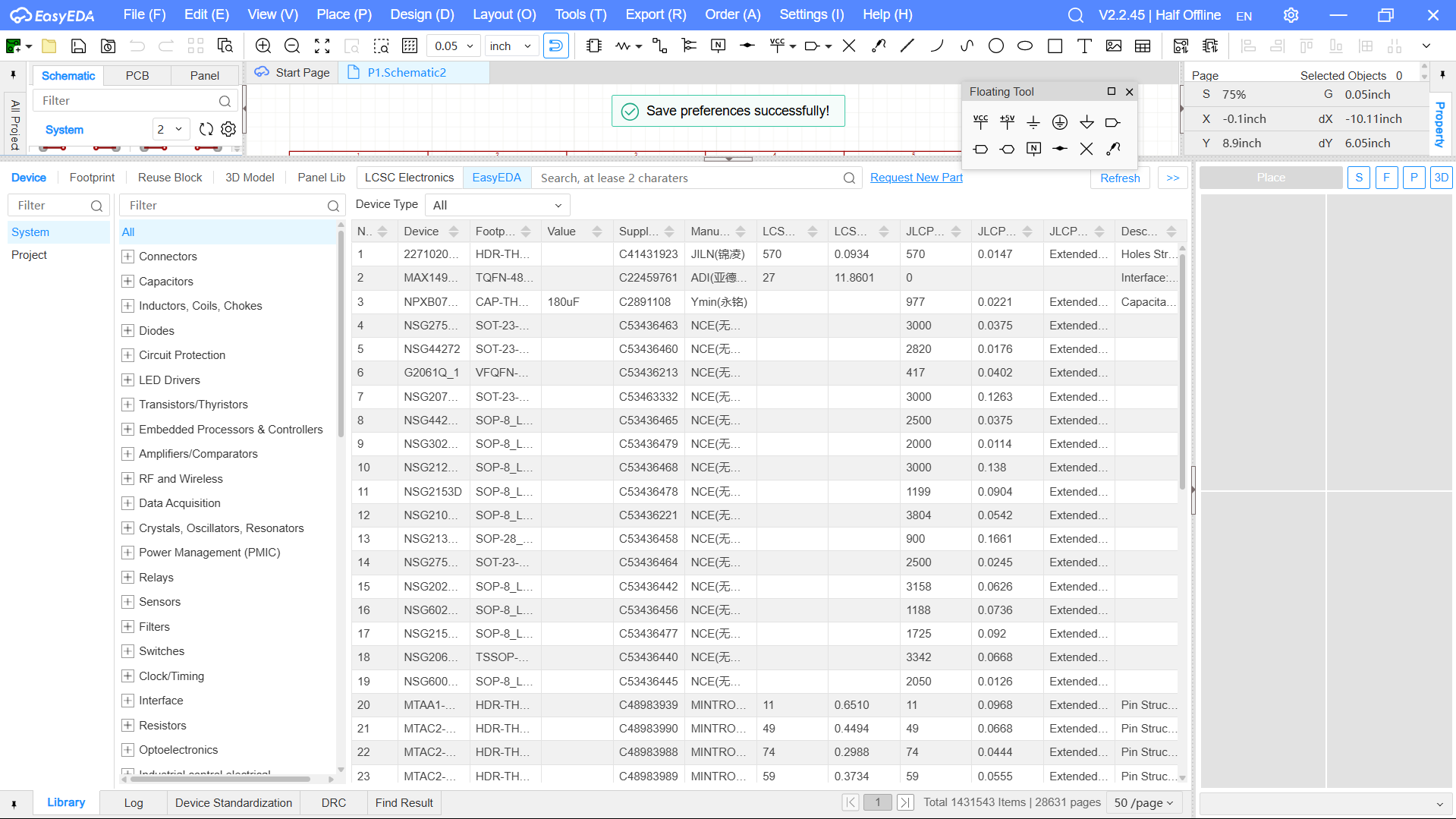
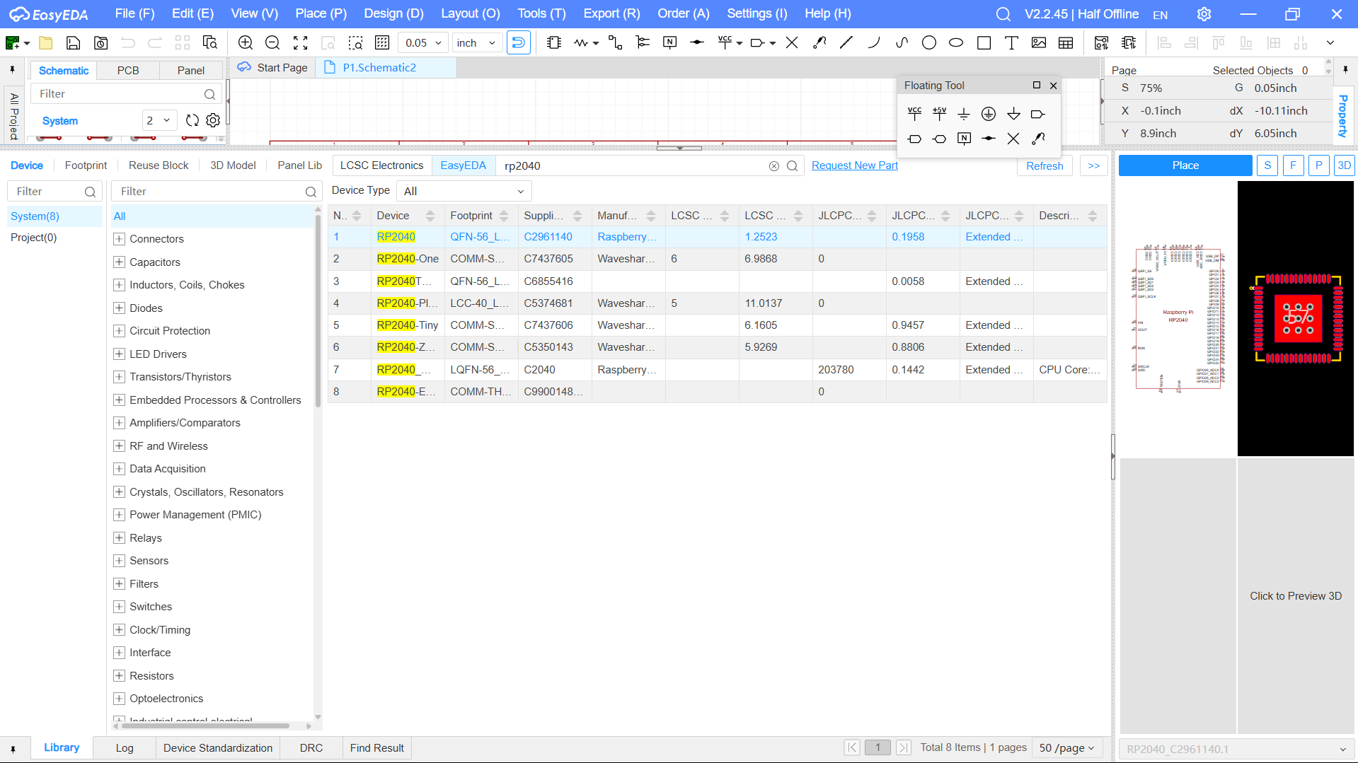
The required components were selected using the EasyEDA component library. I searched for each component individually before placing them into the schematic.
Components Used
| Component | Purpose |
|---|---|
| Seeed XIAO RP2040 | Main microcontroller |
| 10-pin Female Headers ×2 | GPIO breakout |
| Push Button | User input |
| LDR | Light sensing |
| LED | Output indicator |
| 470Ω Resistor | Current limiting |
Building the Schematic
I began by placing the Seeed XIAO RP2040 at the center of the schematic. From there, I gradually added the supporting components required for the circuit.
- Placed the Seeed XIAO RP2040.
- Added two 10-pin female headers for GPIO breakout.
- Added a push button for user input.
- Added an LDR as a light sensor.
- Added an LED with a 470Ω current-limiting resistor.
- Connected all GPIO, power and ground connections.
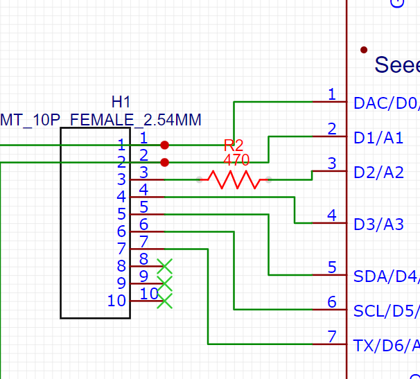
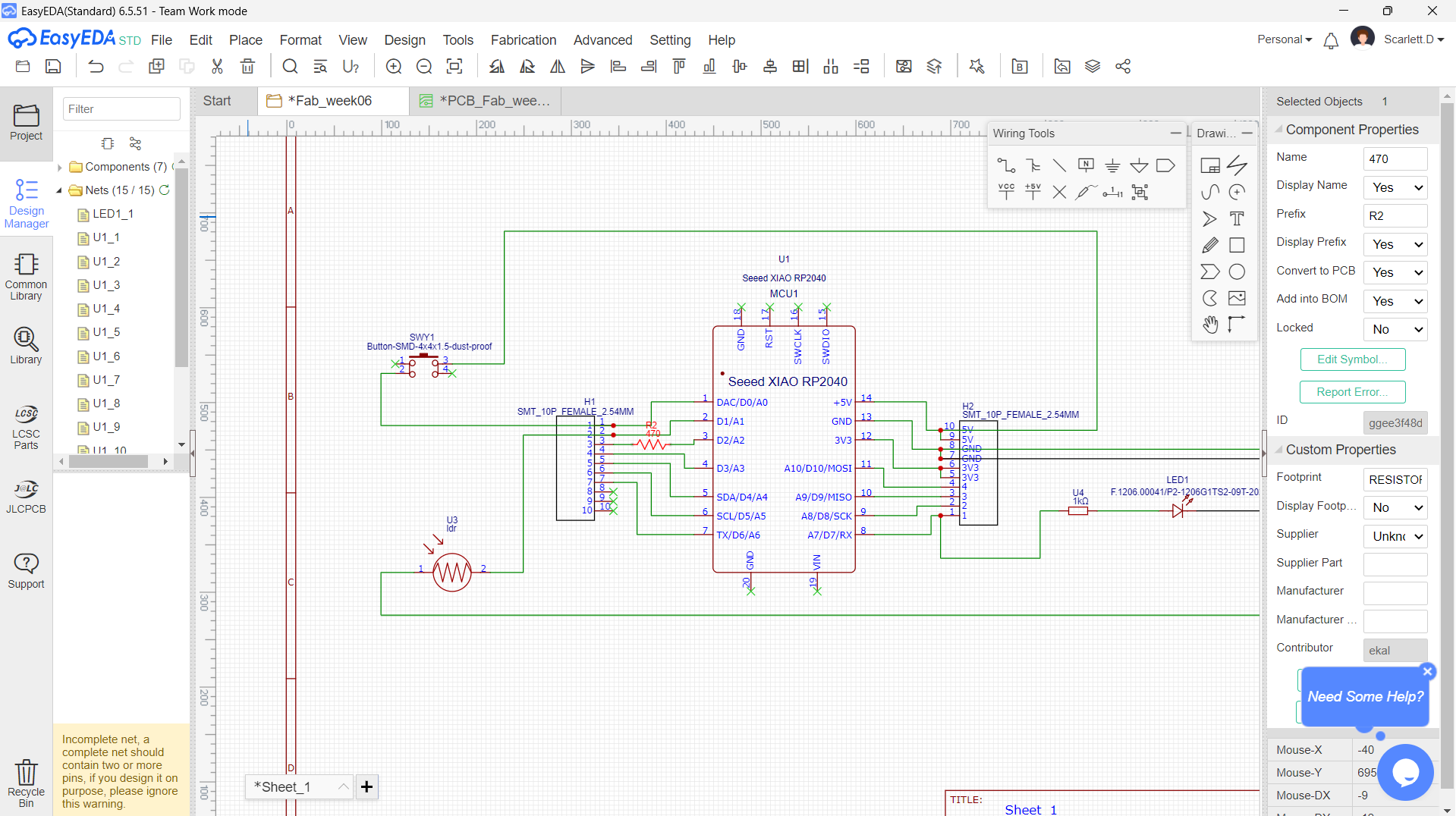
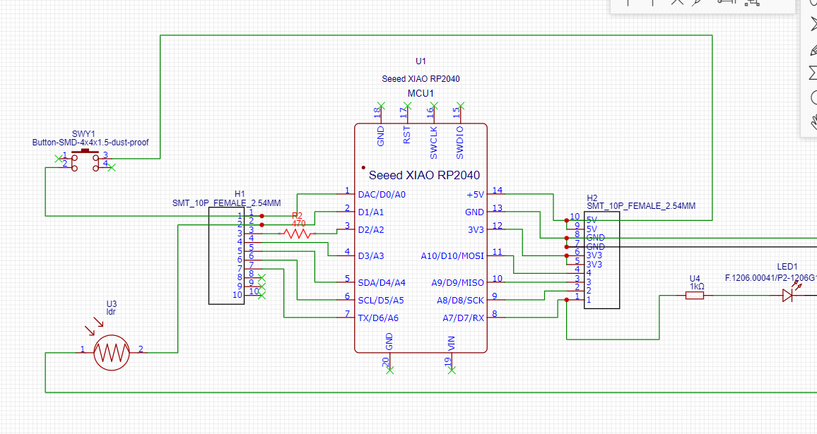
The final schematic provided a complete representation of the embedded system and was ready to be converted into a PCB layout.
PCB Generation
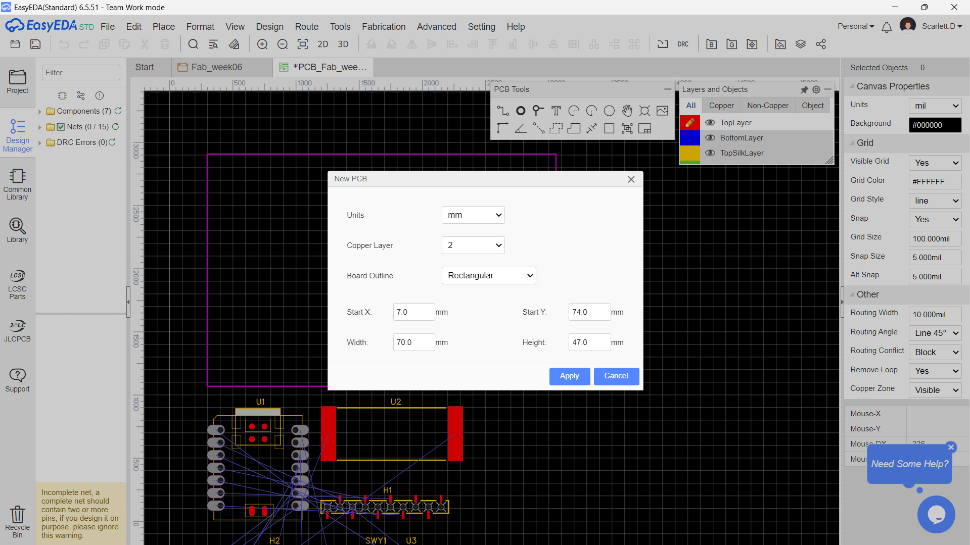
Once the schematic was completed, I converted it into a PCB layout. EasyEDA automatically assigned footprints to every component and transferred them into the PCB workspace.
PCB Layout
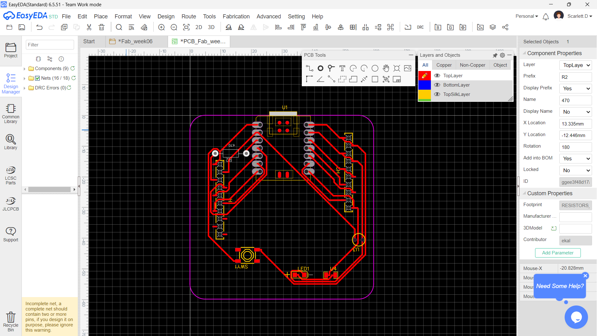
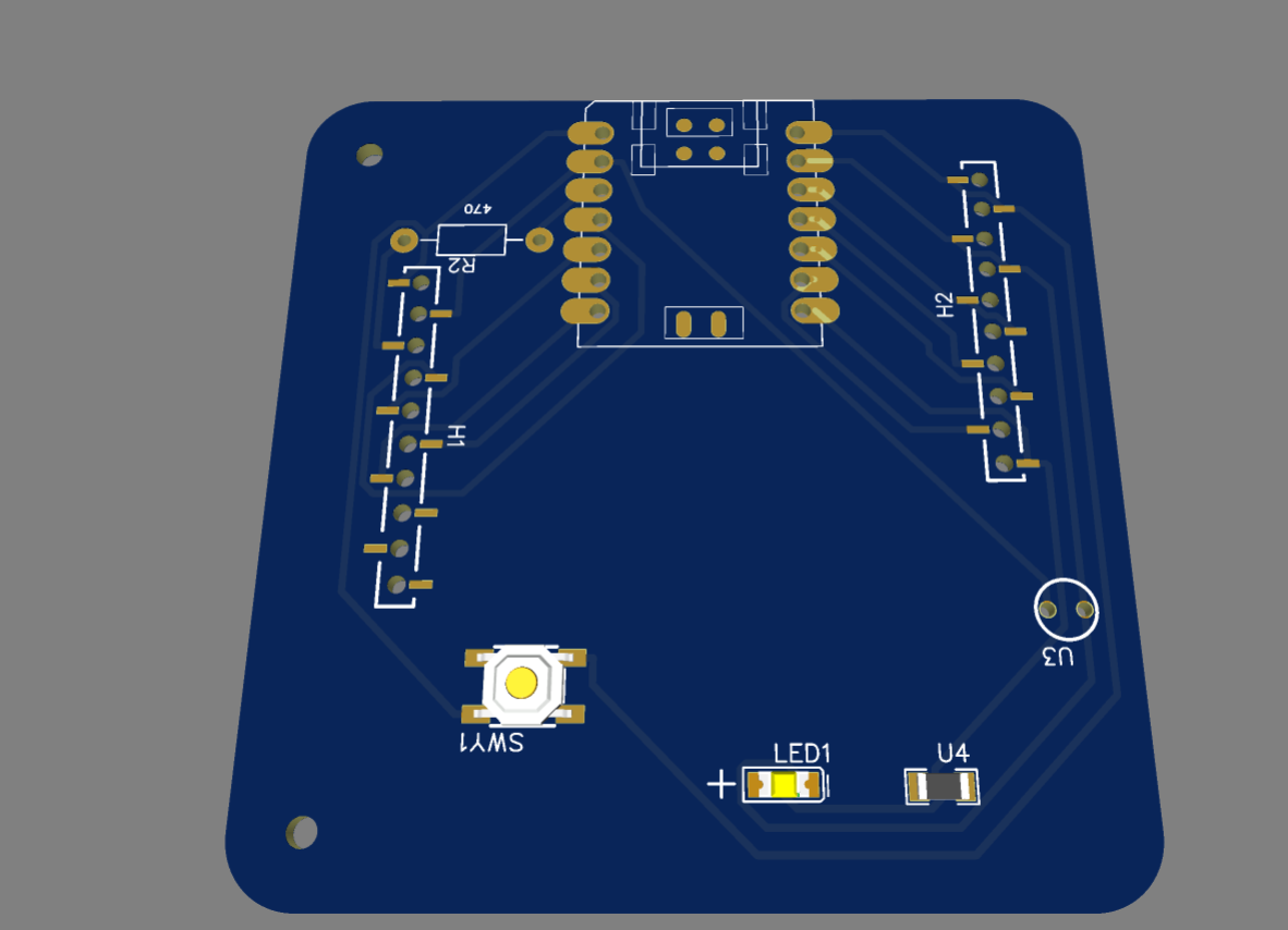
Before routing the traces, I arranged the components to create a compact layout with minimal trace crossings. The GPIO headers were placed on either side of the RP2040 while the LED, resistor, push button and LDR were positioned around the board.
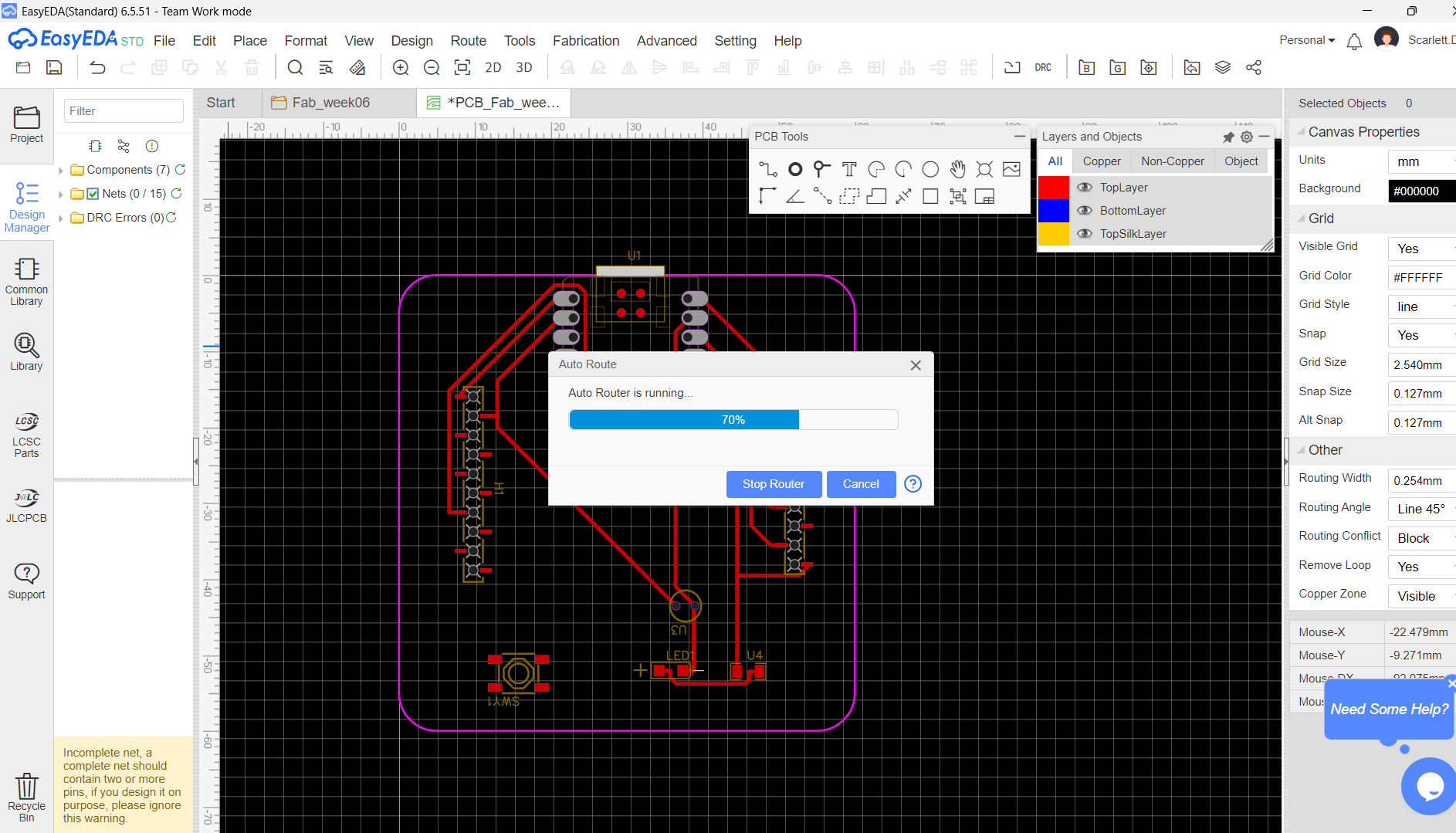
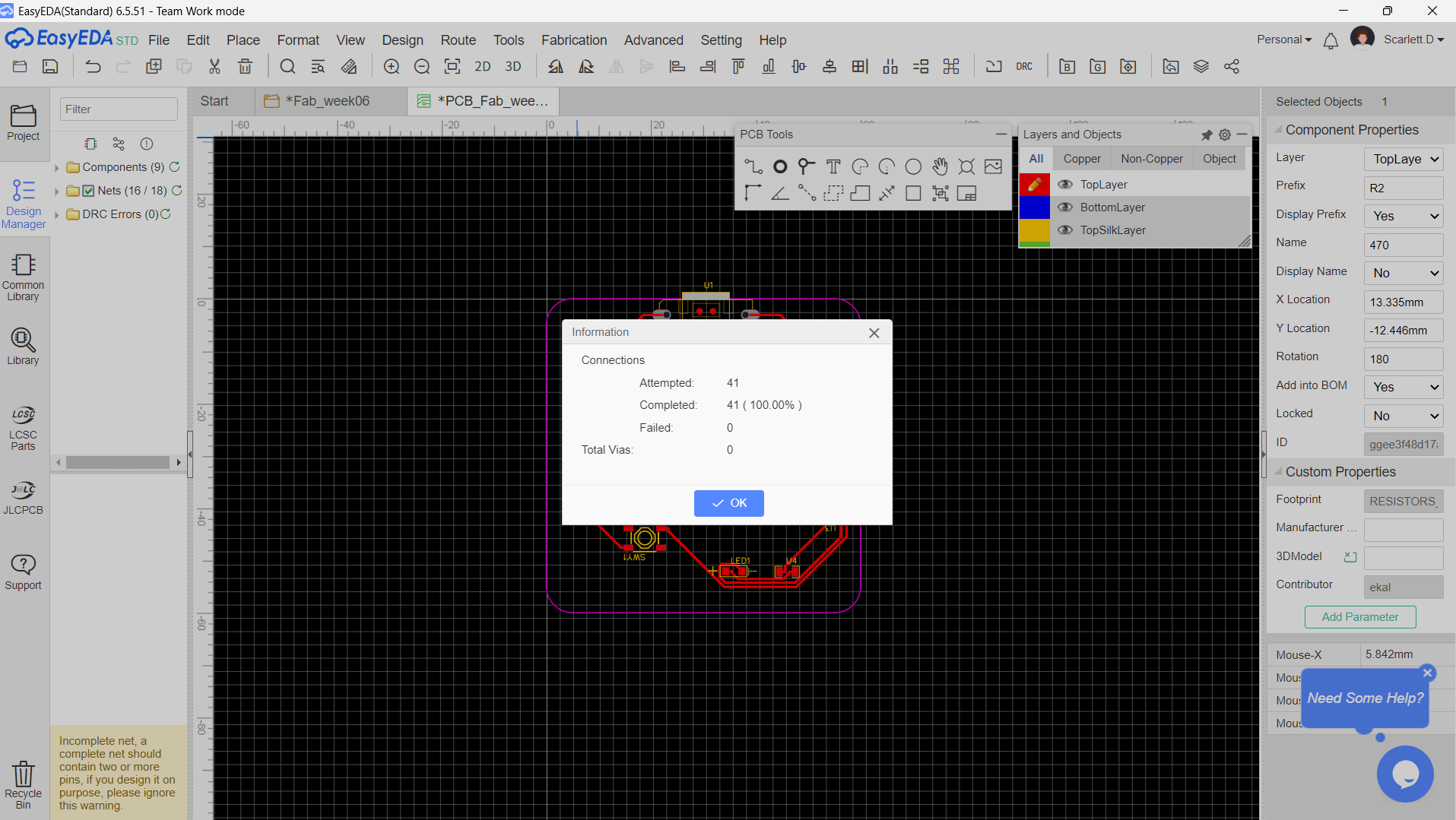
After positioning the components, I routed the electrical connections between them. EasyEDA provides both manual routing tools and an Auto Router, which helped generate clean and efficient trace paths across the board.
Throughout the routing process I ensured that traces maintained proper spacing while avoiding unnecessary crossings wherever possible.
Design Rule Check (DRC)
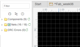
Before finalising the design, I ran the Design Rule Check (DRC). This verifies that the PCB satisfies manufacturing constraints such as trace spacing, pad clearances and routing conflicts.
After making a few routing adjustments, the design passed the DRC successfully without any errors and was ready for fabrication.
Final PCB Design
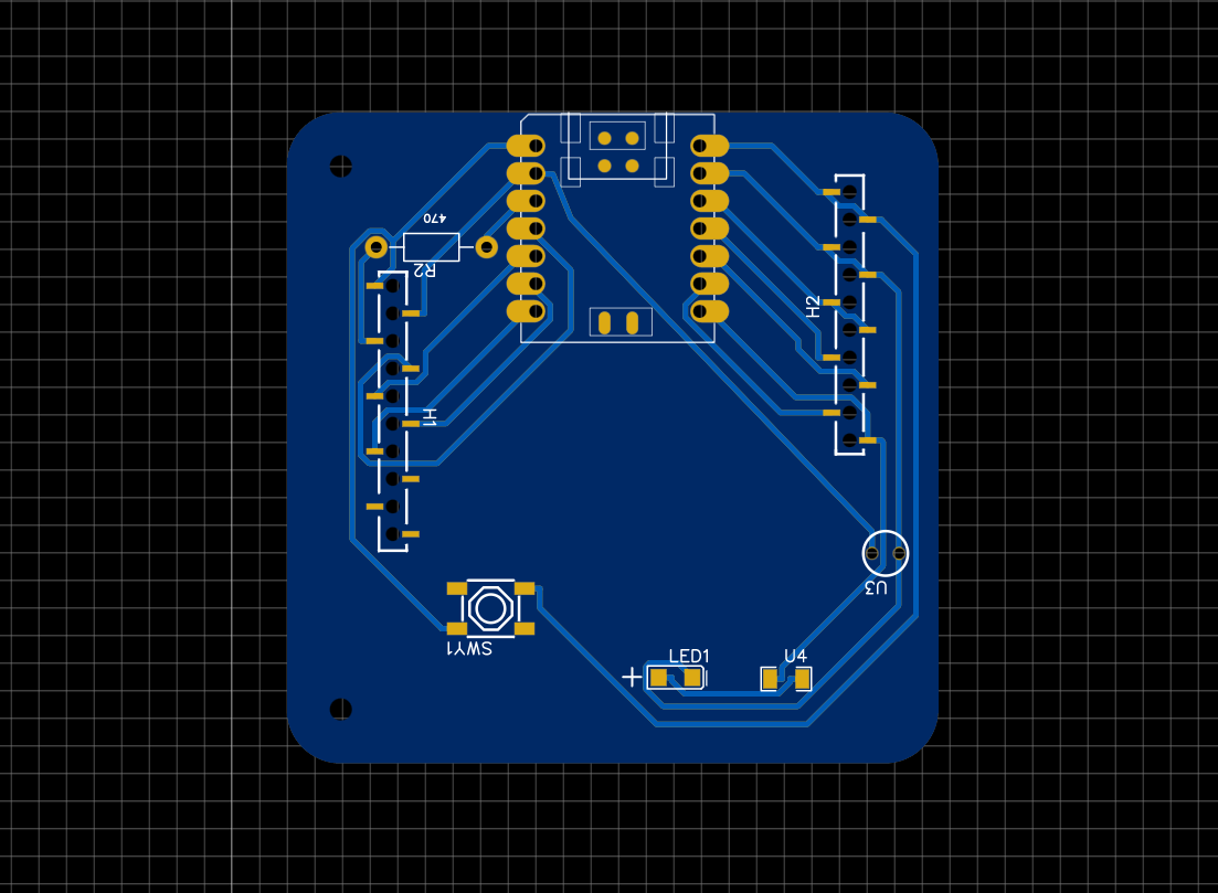
The completed PCB includes the Seeed XIAO RP2040 footprint, GPIO breakout headers, an onboard LED with a current-limiting resistor, an LDR connection, a push button and mounting holes. The traces were routed to create a compact and organised layout suitable for fabrication.
Reflection
This week introduced me to the complete PCB design workflow. From selecting components and building a schematic to routing traces and verifying the design using DRC, I gained a much better understanding of how an electronic circuit is translated into a manufacturable PCB. Although the board was not fabricated during this week, I finished with a design that was ready for production in the following week's assignment.
📁 Design Files
Gerber FilesJSON File