Week 08: PCB Design and Milling
Assignment brief:
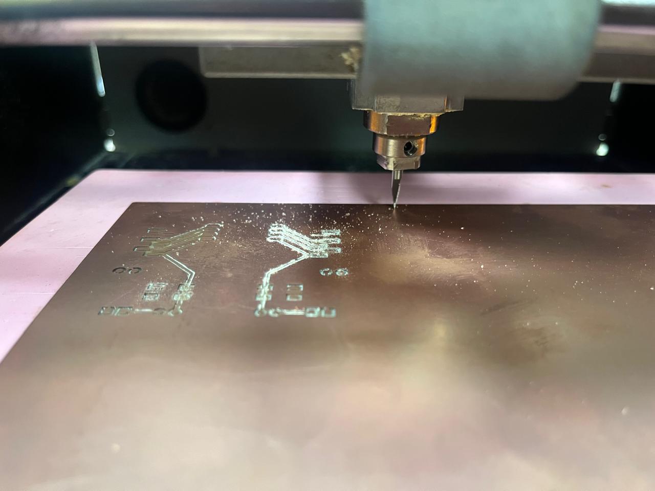
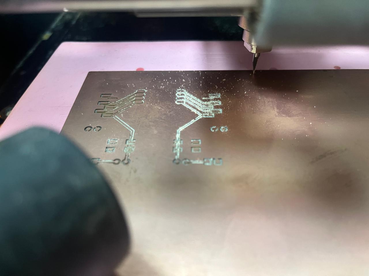
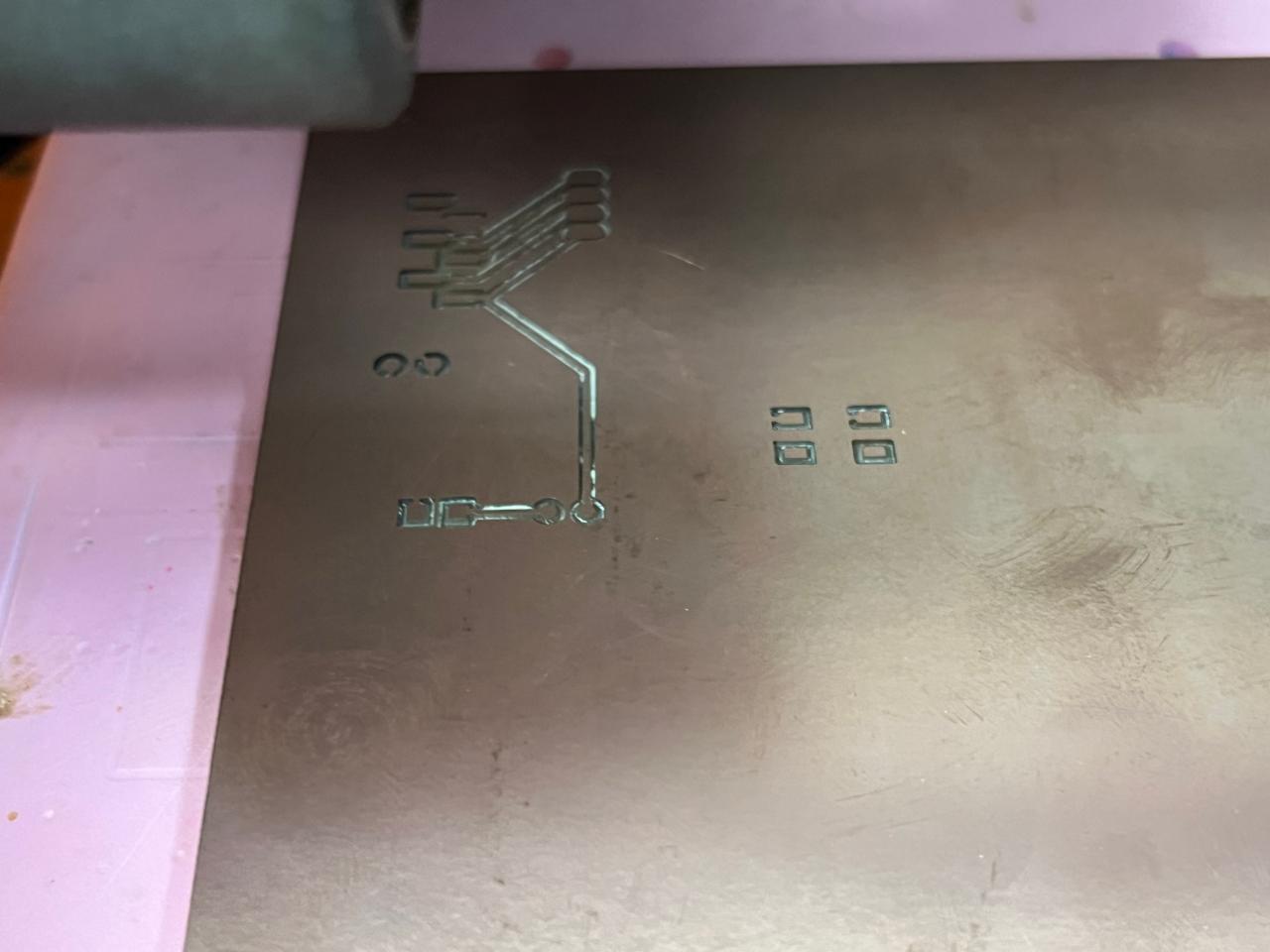
This week’s group assignment was to characterize the design rules for our in-house PCB production process. This involved documenting key machining parameters such as feeds, speeds, plunge rate, and depth of cut for both traces and board outlines, as well as identifying the tooling used for milling.To understand the process better, we reviewed previous work from earlier students. This helped us get a clearer idea of the workflow and the steps required. We also found reference designs for clearance test patterns, which are commonly used to determine the minimum trace width and spacing that our milling machine can reliably produce.
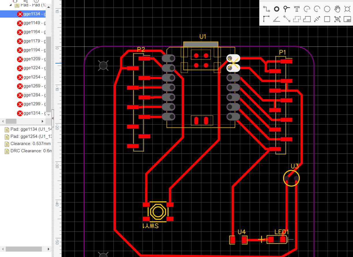
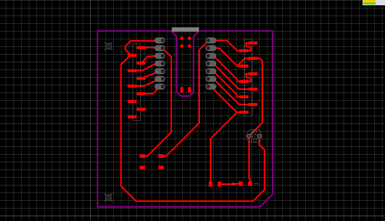
Designing the PCB
I had to make some iterations to my design before exporting as I came across a few challenges in CopperCAM.
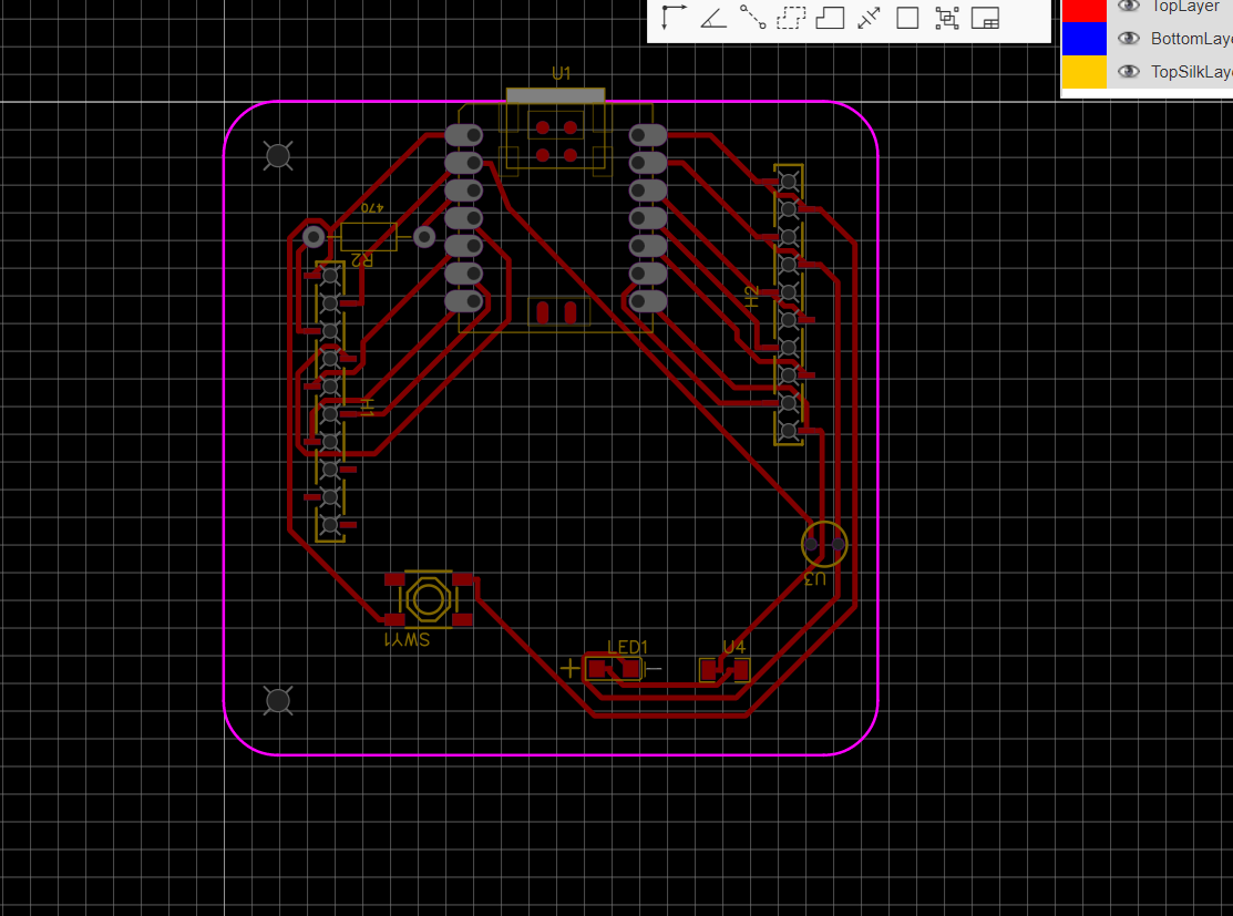
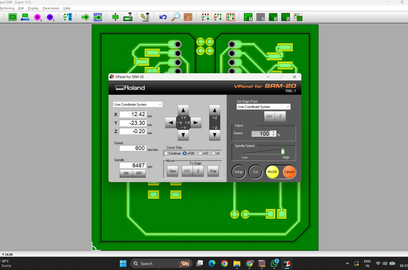
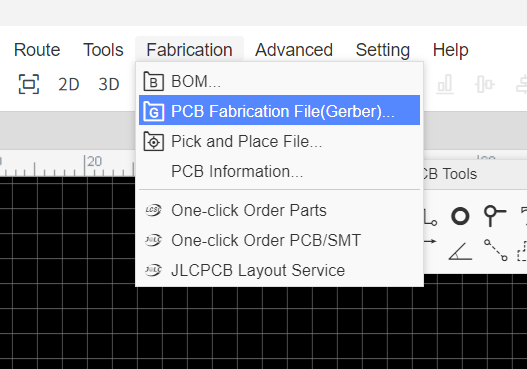
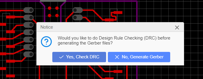
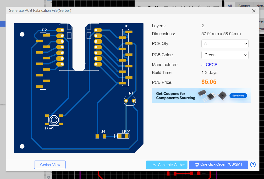
We export Gerber Files into CopperCAM from EasyEDA.
To export Gerber Files:
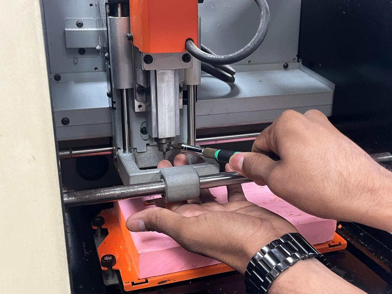
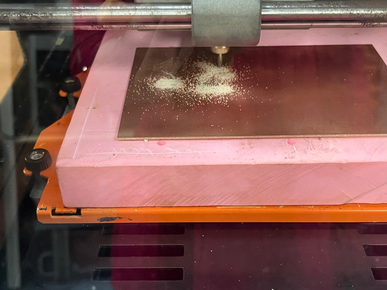
PCB Milling Process