Electronics Production
Goals for Week 8:
Document design rules & process of sending traces to the milling machine,
Do the group assignment,
Make and test a microcontroller development board that you designed
Group assignment page:
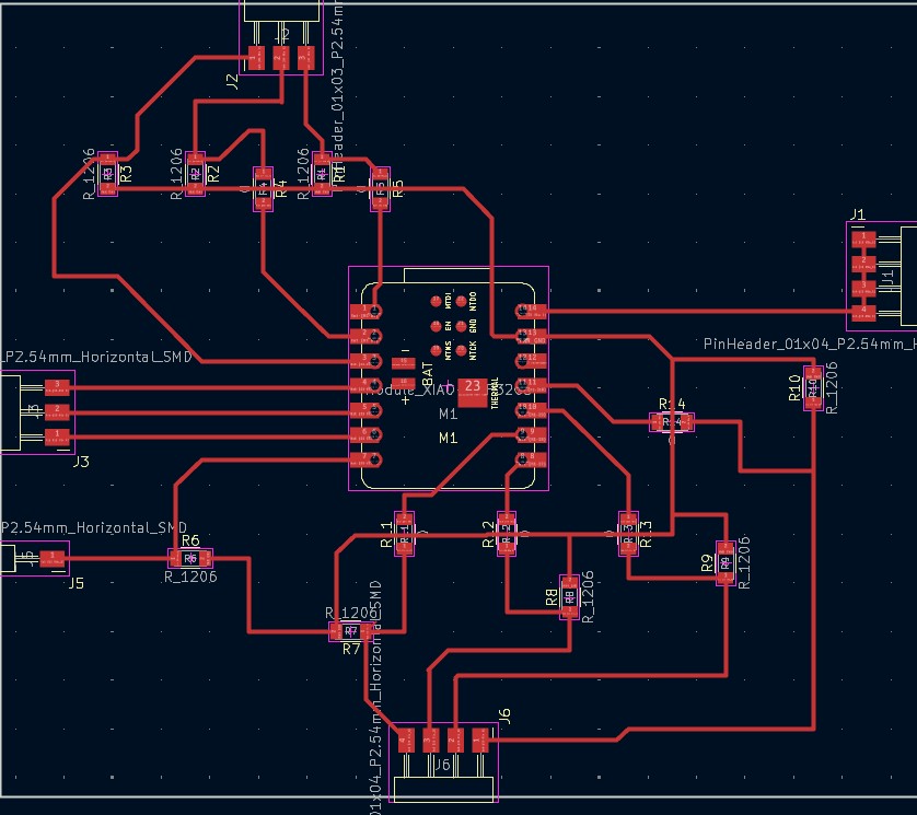
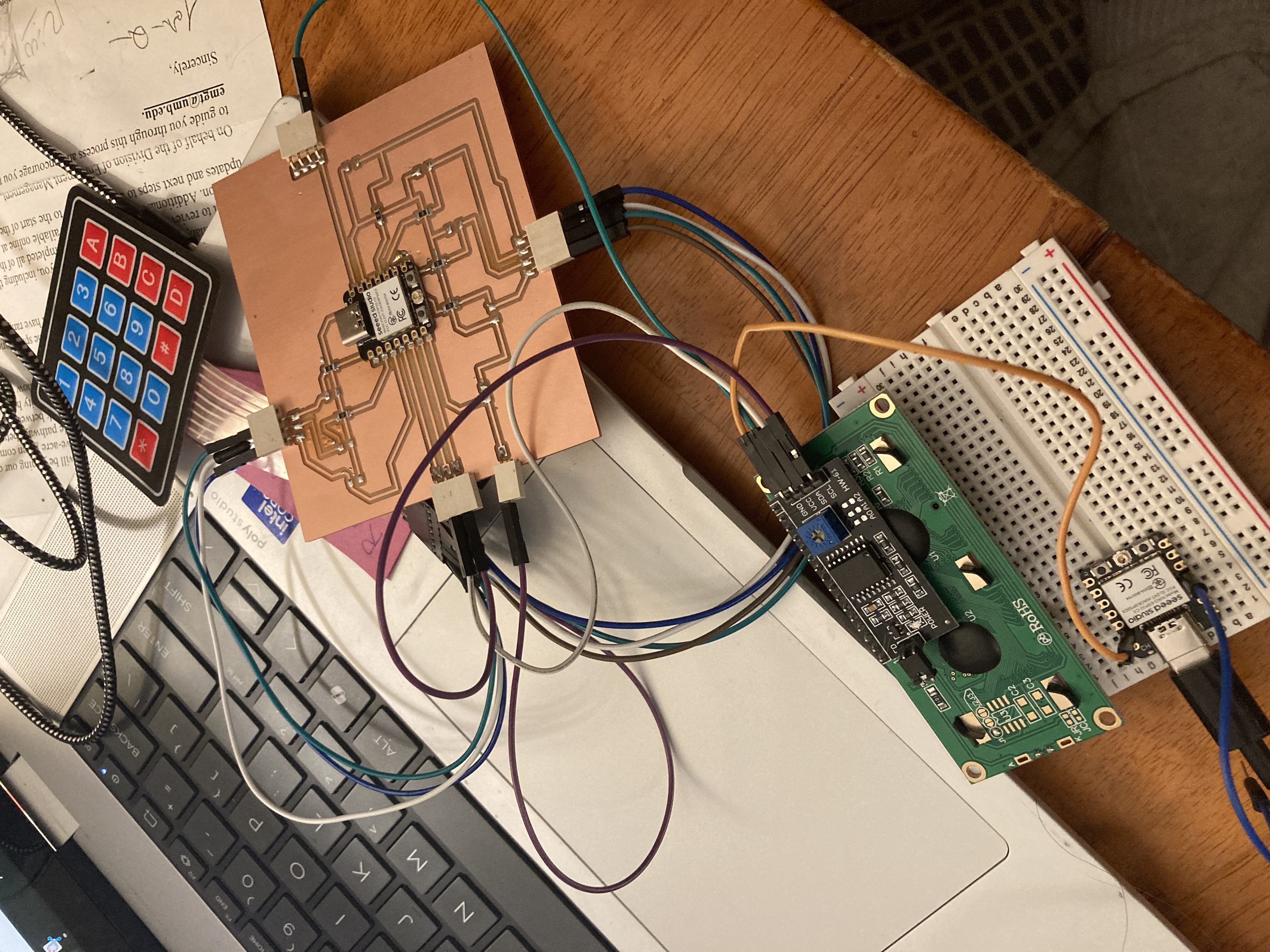
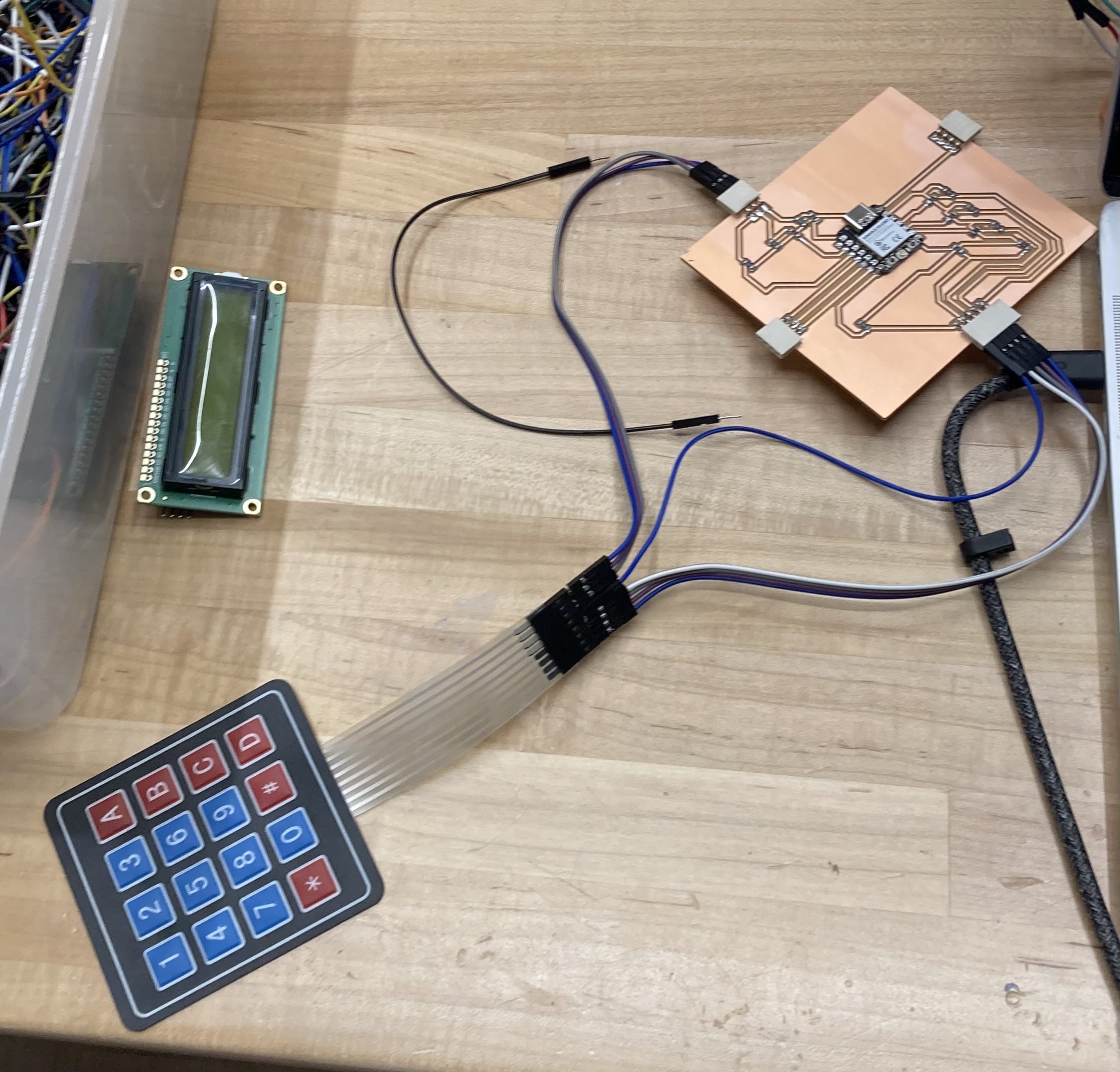
Developing the Xiao ESP32 C3 board
Edge cuts file
Traces file
Design Rules
These images show a line test used to determine the minimum trace width and spacing that can be reliably milled on a PCB using our current setup. The labels (.001, .010, .020) refer to the trace widths and spacings in inches. By comparing the digital design with the milled result, we can see that the .001" features are too fine and result in poor quality traces or bridging, while the .010" region shows improvement but still some imperfections. The .020" region mills cleanly and consistently, indicating it's within our tool’s reliable capability. Based on this test, our minimum trace width and spacing should be at least 0.010", though 0.012" or more is safer for consistent results. We can use this information to set design rules in our PCB software to avoid creating features too small for our mill to handle.
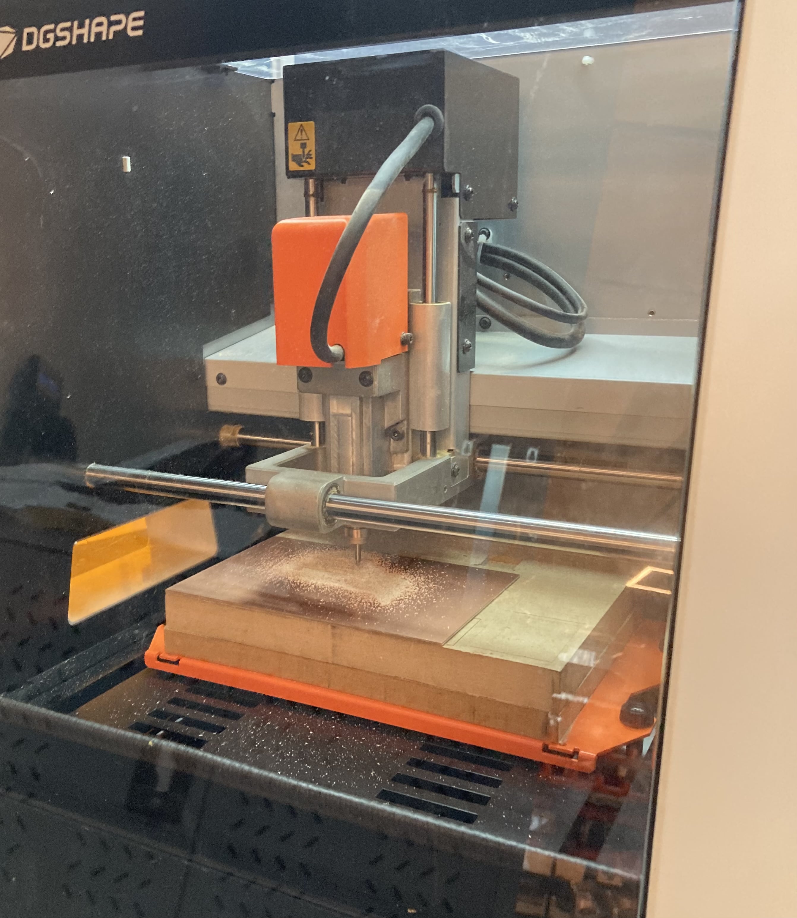
While 10 mm/s speed is standard, the tip of the endmill kept snapping off halfway through the job. To fix this, we changed the speed from 10 mm/s down to 6 mm/s for the traces.
Use the document below to understand how to export the board from KiCad all the way to uploading the files to VPanel for cutting.
Use this link to access mods.

