
The Astro AI digital multimeter was used to measure voltage, current, and resistance in electronic circuits and devices, helping diagnose faults, test batteries, and verify correct voltage levels. We connected the probes properly and used the multimeter to read voltage in ohms, observing measurements in a 5V circuit. The experiments included testing red and blue LEDs with a breadboard setup, where we analyzed forward voltage differences. The blue LED required a higher voltage than the red, demonstrating how resistance affects current flow and LED brightness. Using an oscilloscope, we visualized voltage fluctuations in an Arduino-controlled LED circuit, observing square waves due to rapid on-off switching. While we did not use transistors, we noted that MOSFETs are preferred over BJTs in many applications for their efficiency and ability to precisely control current. These experiments enhanced our understanding of circuit components and measurement tools.
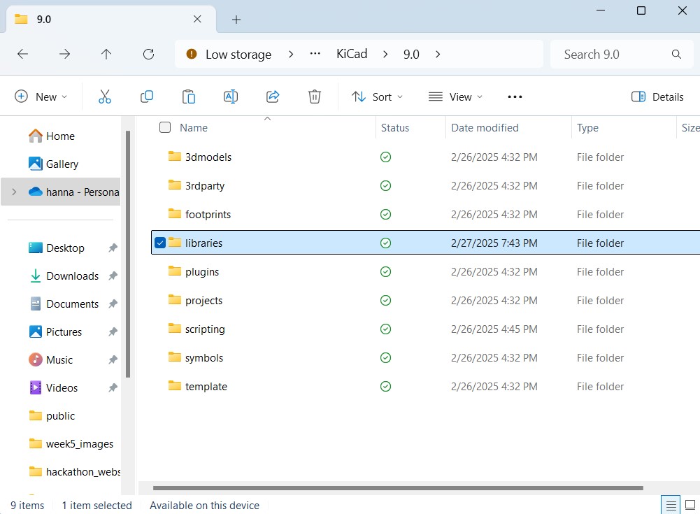
First, we installed the fab library at this file location.
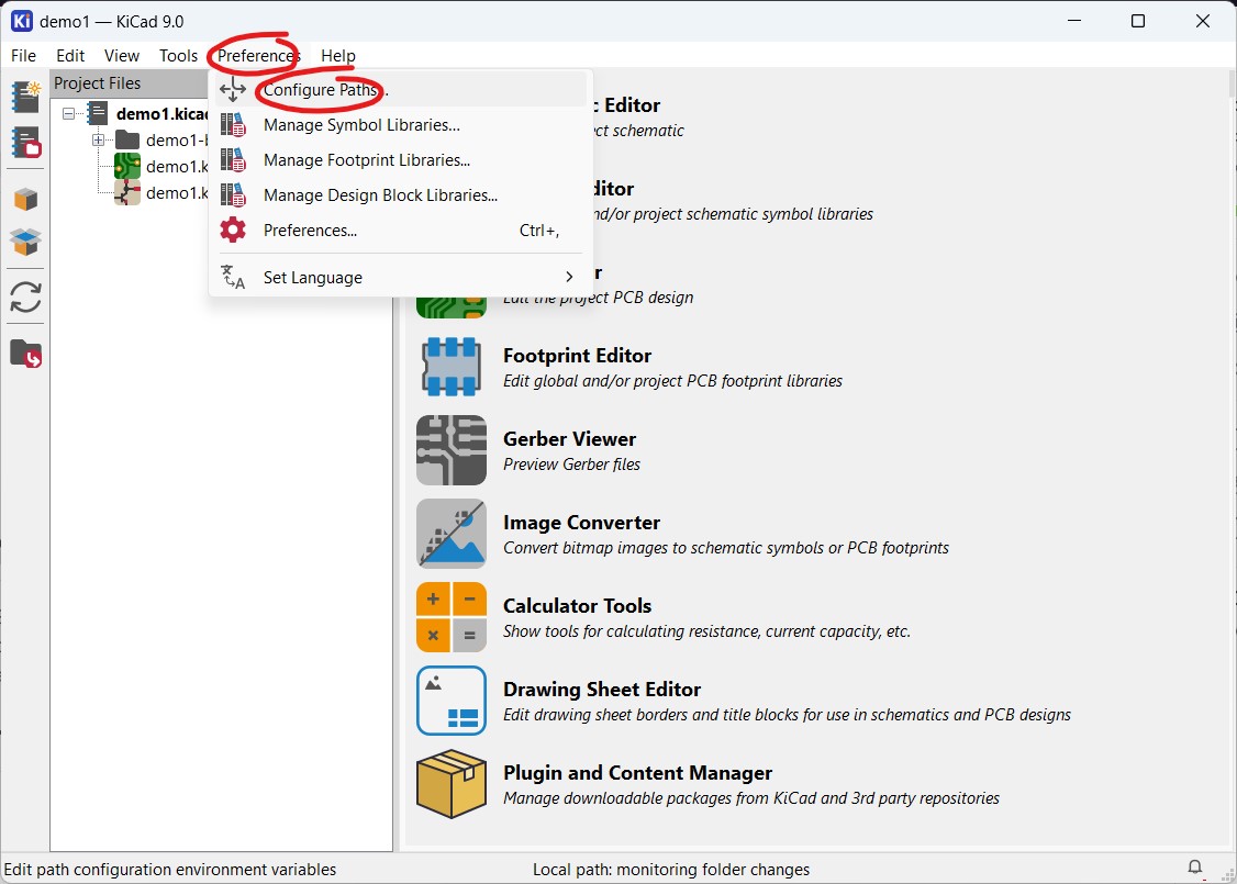
In order to have the symbols from the fab library actually show up, we clicked Preferences > Manage Symbol Libraries.
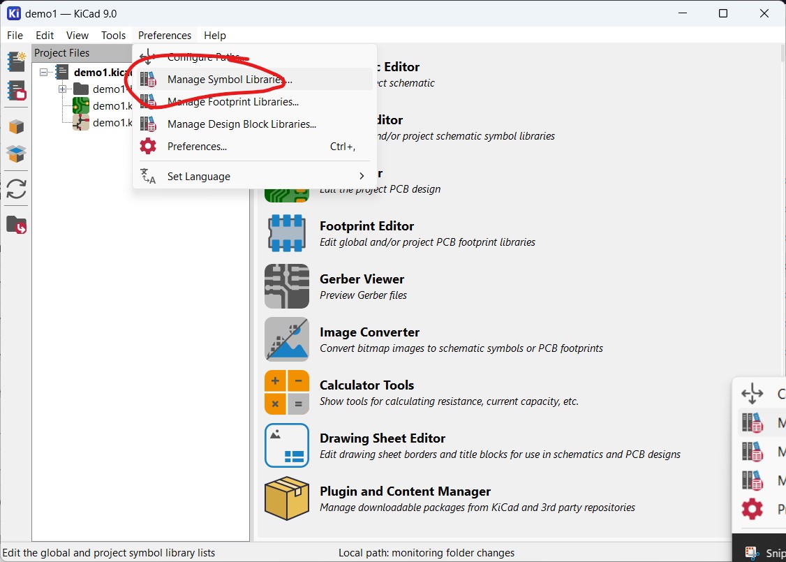
Click the plus button at the bottom, and put in the fab symbol library (fab.kicad_sym). MAKE SURE YOUR NICKNAME IS 'fab' WITH A !!!!LOWERCASE!!!! 'f'!!!!! Your symbol library won't actually import correctly if not.
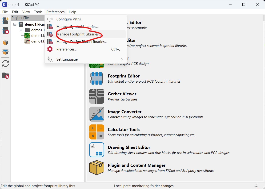
Next, we'll move onto the footprint library. Click Preferences > Manage Footprint Libraries.
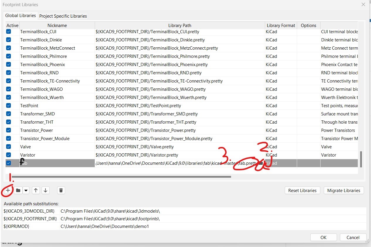
Follow the steps shown in red in the image. Use fab.pretty. Again, MAKE SURE YOUR NICKNAME IS 'fab' WITH A !!!!LOWERCASE!!!! 'f'!!!!! Your footprint library won't actually import correctly if not.
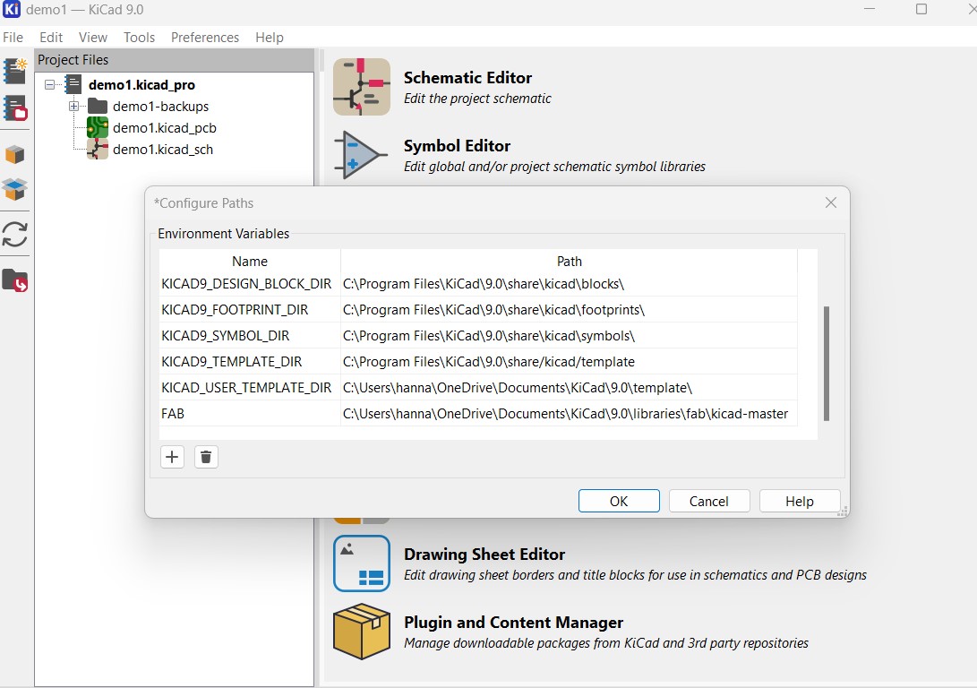
Finally, go to Preferences > Configure Paths
Press the '+' button, and add 'Name' FAB with the path including kicad-master. Click 'ok'. We should be fully set to start designing with the PCB and schematic editors.
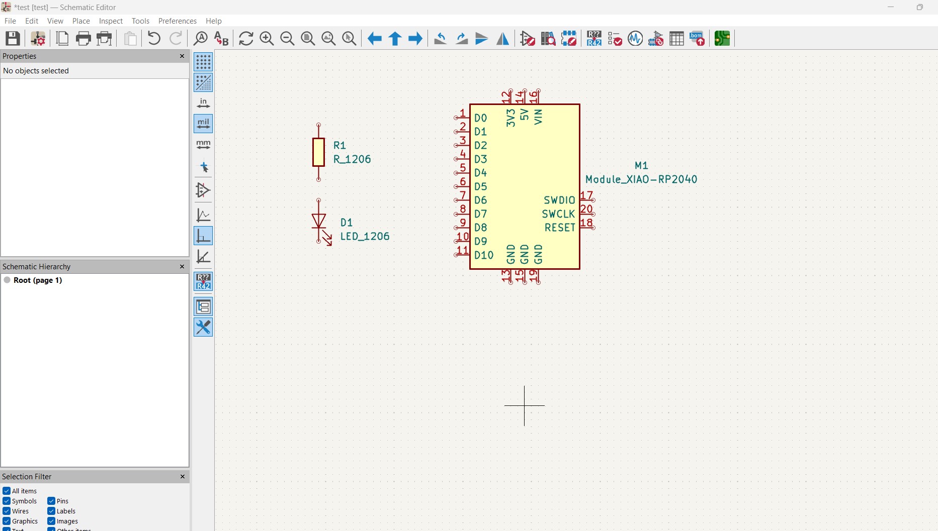
The basic components for the circuit we made in class.
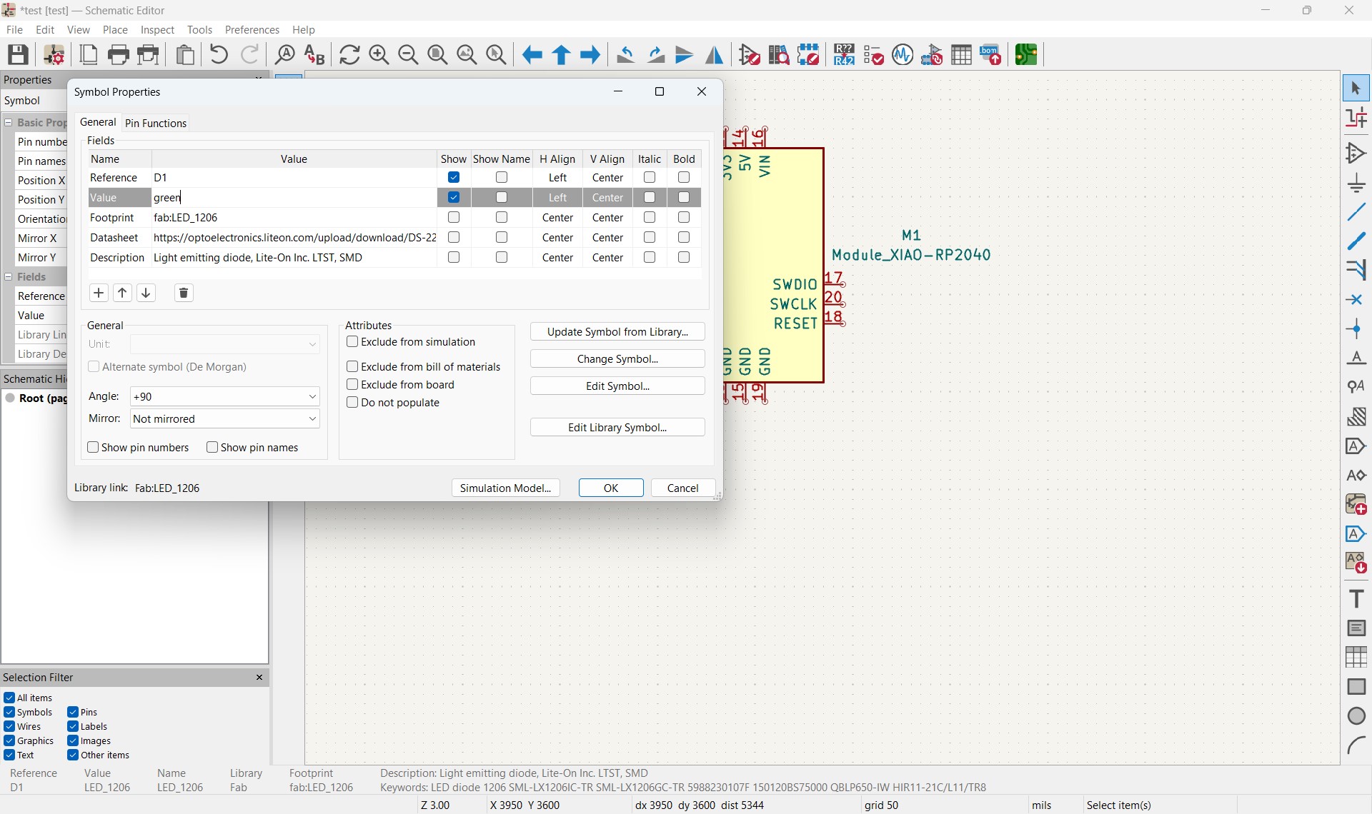
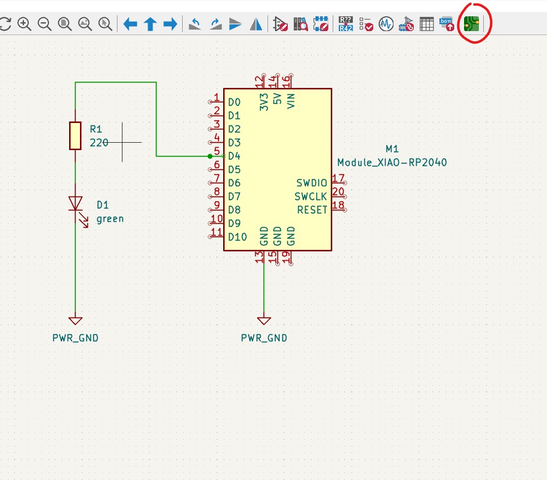
How to change the value of a component (Symbol Properties, left menu).
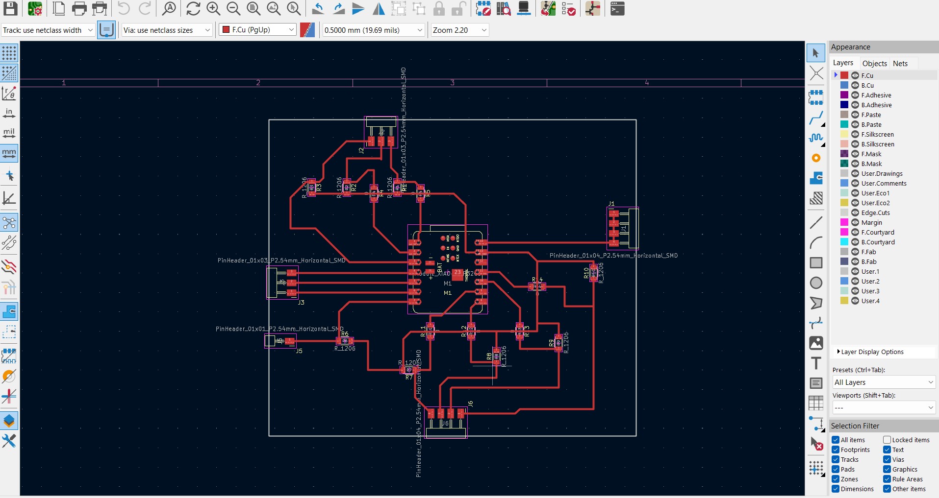
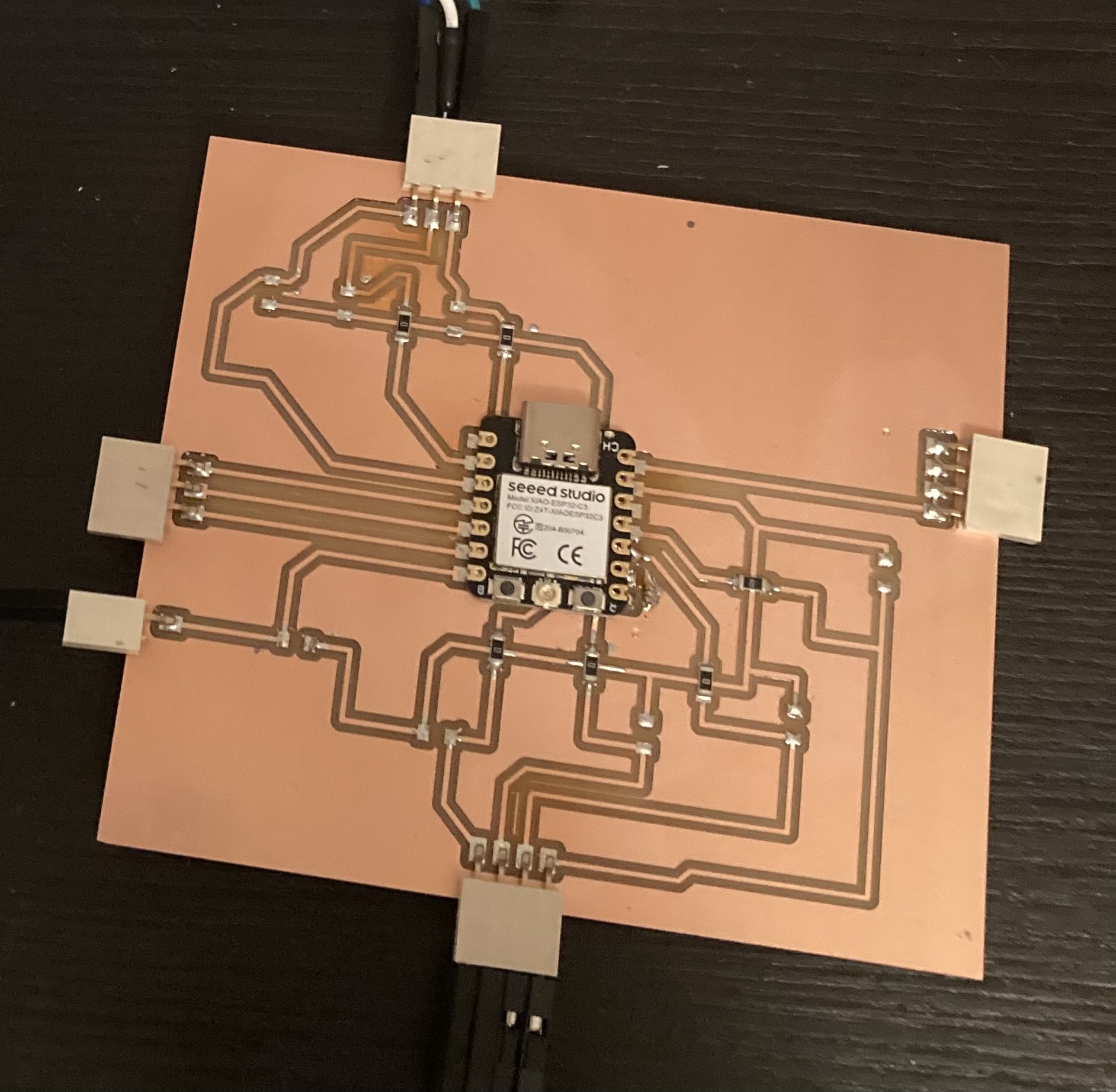
The finished circuit in schematic. We can switch to PCB by pressing the button circled in red.
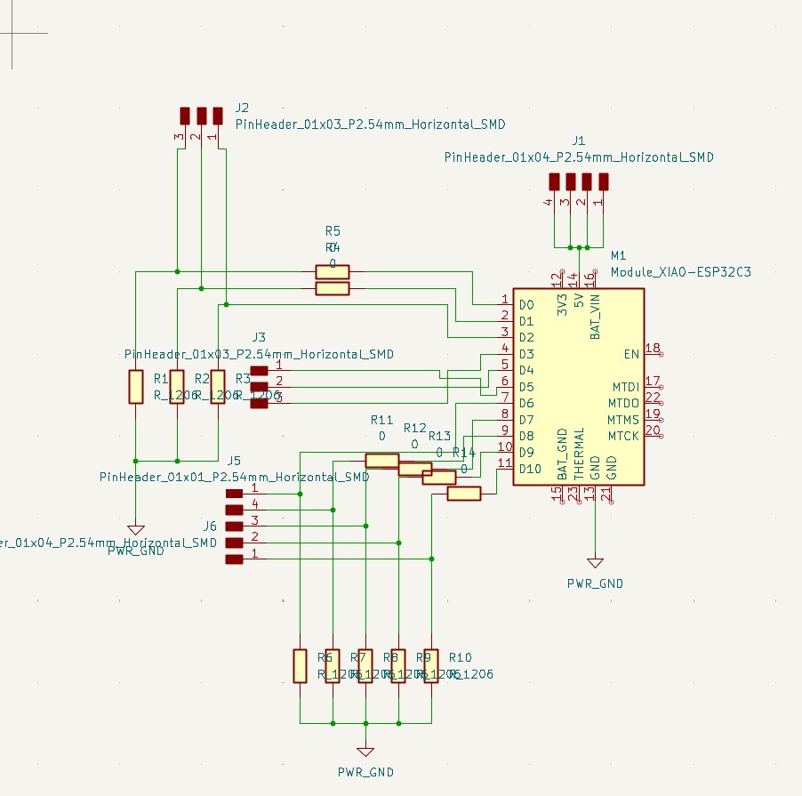
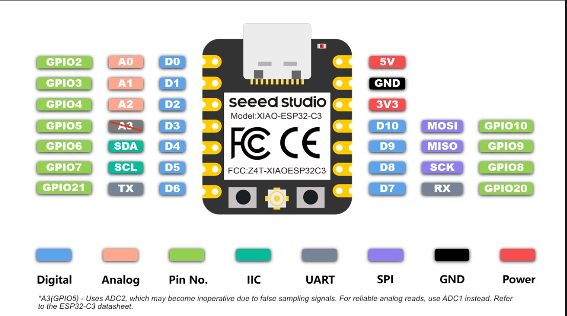
To make a keypad and LCD screen design, I realized that I would need at least 12 pinheaders. 8 for the keypad, and 4 for the lcd display. Importantly, the lcd display needs a 5V and GND connection. The lcd screen also needs 2 I2C pins. The keypad just takes 8 digital pins. I made my traces to the ESP32 with this in mind for sure.
Use the document below to understand how to export the board from KiCad all the way to uploading the files to VPanel for cutting. Use this link to access mods.