6. Electronics Design - Week 6
6.1. Assignments
Electronics Design
group assignment
use the test equipment in your lab to observe the operation of a microcontroller circuit board
individual assignment
use an EDA tool to design a development board
that uses parts from the inventory to interact
and communicate with an embedded microcontroller
extra credit: try another design workflow
extra credit: simulate your design
extra credit: design a case around your design
6.2. Group Assignment
6.2.1. Learnings
Labratory Power Supply
constant current (CC) and constant voltage (CV) mode
usually in CV but if used current exceeds limit, power supply changes -> issue in board
always disconnect, when changing circuit!!
Oscilloscope
all about the trigger level (current)
if above level, it will ‘trigger’ a periodic signal and synchronizes the horizontal visualisation
3 modes: auto, normal, once
auto: triggers automatically if above level, showing signals continuously
normal: shows overlapping signals until trigger over level, then records all horizontal, not overriding the current view
once: triggers only one time when reached level
cool use case: use the trigger on a pin of a microcontroller to measure a loop time by setting this pin high
then use the analysis tools to determine the time between voltage goes high and pin goes high for turn on time and high to high of the pin for the loop time
many functionalities integrated for functional/stochastic analysis
cursor for checking a point in the graph, very useful for time measurement in a signal
some include logic analyser which can decode some simple protocols like SPI or I2C
probes can have different values (1x, 10x)
is a scaling factor, try to use a high one to not damage your circuit, and if it is to inaccurate, use a lower one
have an adjustable capacitor you need to calculate (use the rectangular signal from the oszi, if it has one), so that a rectangle looks like one, and not like a typical capacitor curve
6.2.2. Notes
Arduino
not precise voltage, if from laptop
Brown-Out Point: voltage level, where it shuts down due to under voltage
6.3. Individual Assignment
6.3.1. Electronics Design
different packages for components to consider
through hole, surface mount
and those have all different footprint!
width and material thickness importend for tracing, especially for production
always check ERC (Electrical Rule Checker) and DRC (Design Rule Checker)
user ground-planes for heat dissipation
6.3.1.1. Design-Rules
Placing components
similar parts, similar orientation
SMD-parts on one side
when only producing one sided boards, through hole components on the other side -> rotate components footprint
small components one the outside, so they are not shadowed, if possible
Tracing
short, direct paths
always 45°
trace powerline tree-like
signal-trace possibly not branch out
adjust width of traces for needed current
distinct between analog and digital ground
6.3.2. KiCAD Tutorial
6.3.2.1. Tutorial Notes
KiCAD version 8 because in Version 9 SVG-Export does not work with the fab-libraries
General
VSS .. digital ground
VSSA .. analog ground (usually same ground as VSS)
R == Ohm
VDDA most more sensitive (analog voltage)
NRST .. Reset Pin, where N denotes negated
Crystal usually GND24 (ground on 2 and 4)
FootPrints .. physical layout of components used on PCB
importend for buying parts and very importend for connectors
decopling capacitor
close to circuit
for small local energy storage
e.g. when MCU switches, needs quick switch in transient of currents
Filtering
done by resistor, inductor, ferrite bead
ferrite bead behaves resistant at a high frequency (e.g. 120Ohm at 100MHz)
USB
Power rails typically very noisy -> additional filtering (above)
Gerber Files/Manufacturer Output
on project -> export
Schematic Editor
General
Layout in different, logically fitting sections
Flags used to indicate for ERC (below)
like e.g. PWR_FLAG used to indicate a power source from e.g. a filter actual power source
Keys
middle mouse .. Move plane
a .. (A)dd components
ESC .. Cancel KiCAD command
p .. add (P)ower component
e on a component .. (E)dit component
w .. draw a (W)ire (connection)
double click on value symbol (C for capacity, R for resistance etc) .. edit value
double click on component -> click in footprint -> next to it ‘library’
r .. rotate
l .. add (L)able (help when creating a layout)
CTRL+l .. add Gobal lable
x/y .. flip symbol layout vertical/horizontal
q .. places ‘DO NOT CONNECT’ flag (used for rule-check)
m .. (M)ove selected components
‘Insert’-Key .. repeats (only?) dont connect
t .. insert (T)ext
Top Buttons
‘Annotate Schematics’-Button .. change labels of components automatically
‘Electrical Rules-Checker’ .. check for sanity of schematic (ERC)
‘Assign FootPrints’ .. choose the footprints used for your components
in view, right-click on footprint -> view footprint
in view, top left ‘3D View’ (alt+3) -> opens 3D-Model of footprint with component
‘Bill of Material’ to generate Items needed for board
PCB Editor
General
first set board details, like how many layers, have powerlanes?,etc.
‘Ratsnest’ -> lines showing the connection not routed yet
for cutting the board, choose layer ‘Edge.Cuts’
then just draw lines, those then cut the board
you can change the footprint of only the instance clicked on
double click component -> ‘Edit FootPrint’
when near the MCU, try to ‘fin out’ the lanes, so that they are as far from each other
no vias on silkstream
copper zone solid pad -> prevent ‘Tombstoning’??
help connectivity and lower inductions
Board Setup
top left ‘Board Setup’-button
Layers:
Fab .. for assembling the board
Silkscreen .. for text and outlines on the PCB
Mask .. prevent solder bridging
Cu .. copper layer
lower layer mostly power layer -> keep high from low voltage separated
Board finish
Copper finish usually Gold -> ENIG .. Emersion Nickle Gold
Design Rules
dependent on the producer
IMPORTANT to copy those into KiCAD
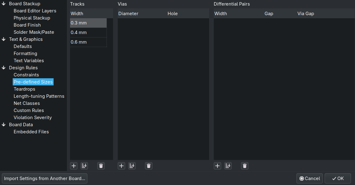
Predefined Sizes
can be used while editing
good defaults:
0.4mm
0.6mm
Keys
Alt+3 .. open (3)D-Viewer
m .. (M)ove components
Ctrl+Shift+m .. (M)easurement
r .. (R)otate
Shift+Leftklick .. select multiple, as usual
double click on component -> in 3d tab, you can change/add 3d models to footprints
Ctrl+Shift+z .. draw a filled zone, used for ground?
set some settings for fill, select, which lane (e.g. ground)
draw outline for zone
when finished, press ‘b’
left buttons ‘Draw Zone Fills’ and ‘Draw Zone Outline’ to toggle zone
x .. start routing
f .. finish routing
v .. make a hole to another layer and then x to create a trace, and v again to go back up, x to trace again (vxvx)
Top Buttons
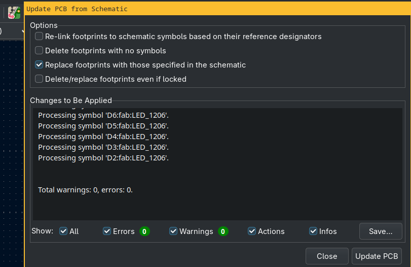
‘Update PCB from Schematics’-Button (F8) to import footprints
‘Design Rules Checker’ again important after finishing
6.3.2.2. Tutorial Outcome
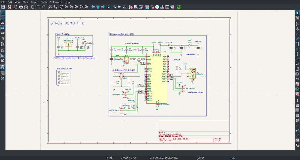
Schematics
Traces
3D Model
6.3.3. Assignment PCB
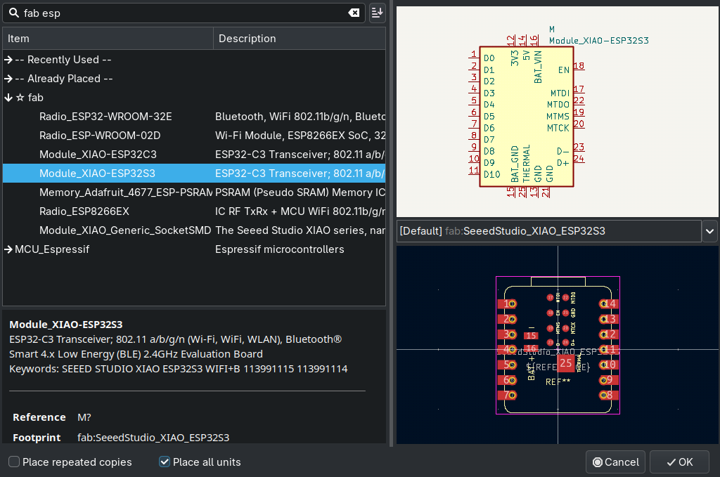
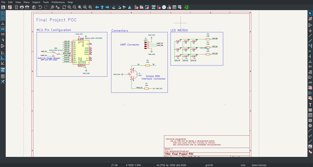
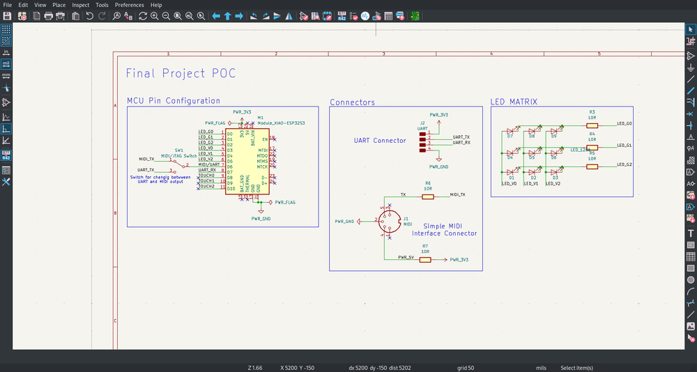
I have chosen to implement a small version of my final project to test a bit to work with MIDI and controlling the lights with it.
I followed the Instructions of the fab library for KiCAD.
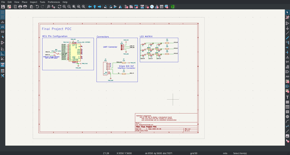
6.3.3.1. Schematics
Designing here is pretty straight forward, just choose your components (a):
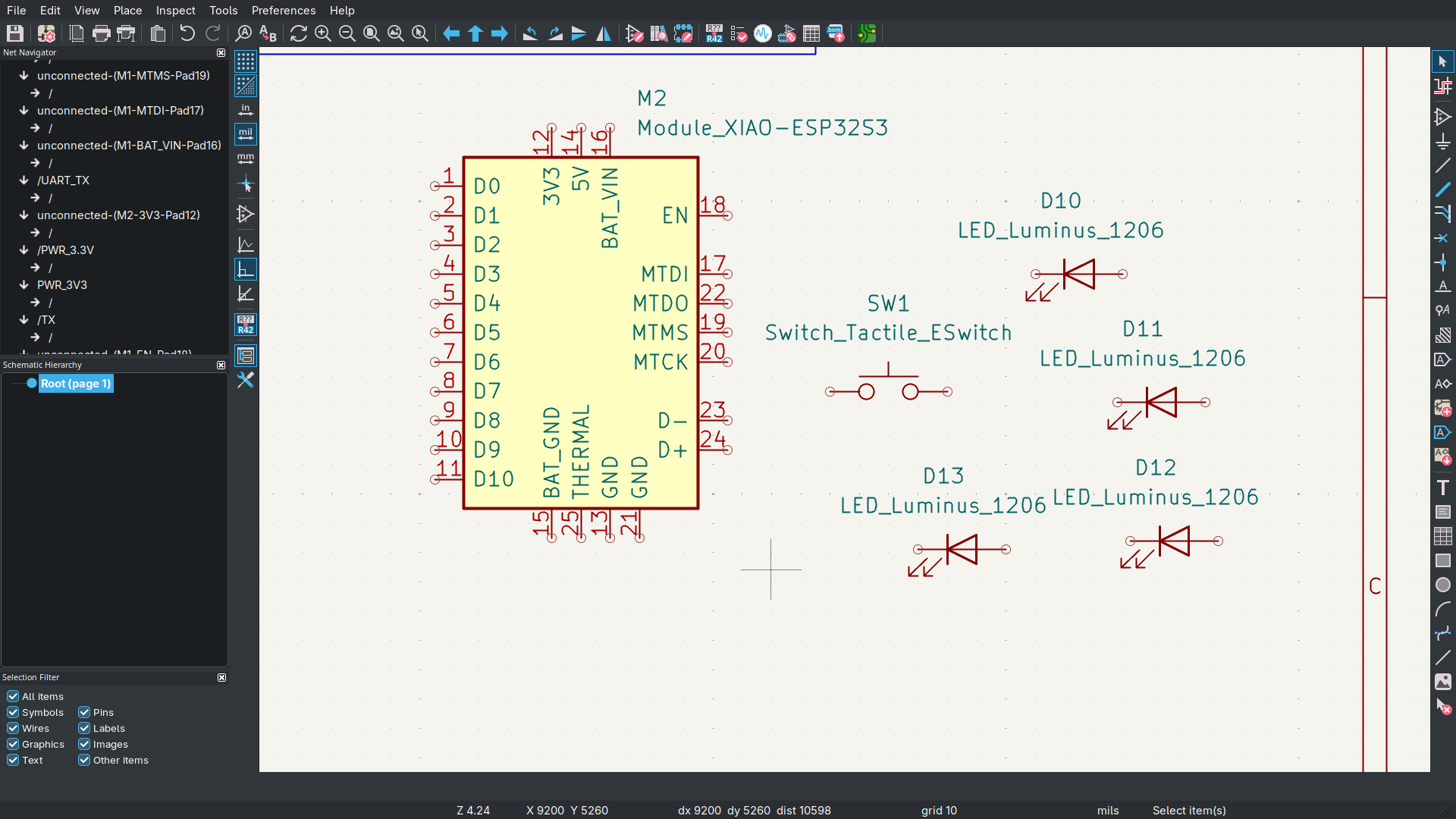
Connect them (w):
Make your structure a bit more clearer:
and run the DRC:
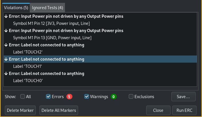
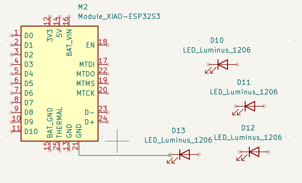
In this case I forgot to mark the power lines from the XIOA as power out and I accidentally marked the touch pins as closed pin:
And now it works:
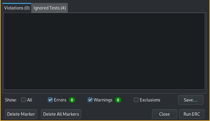
Outcome
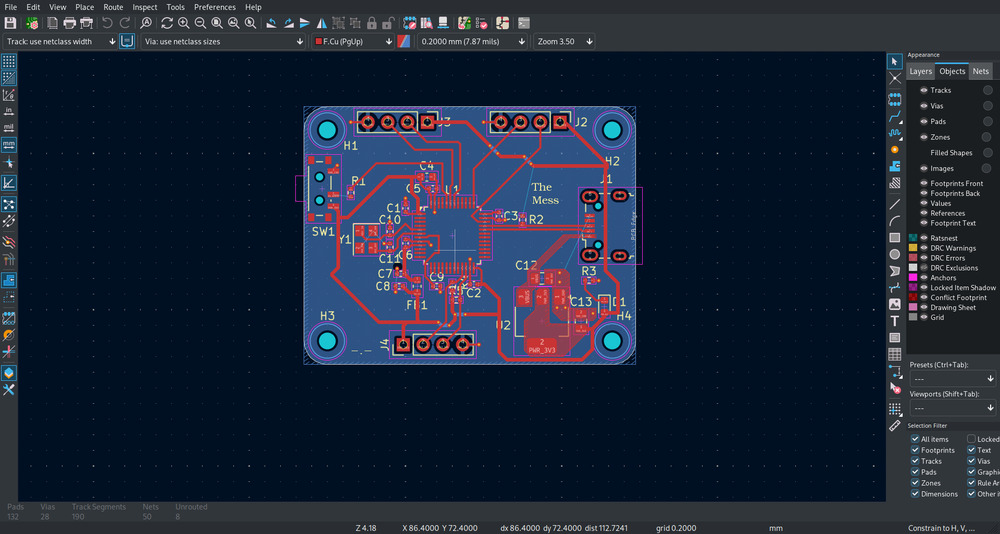
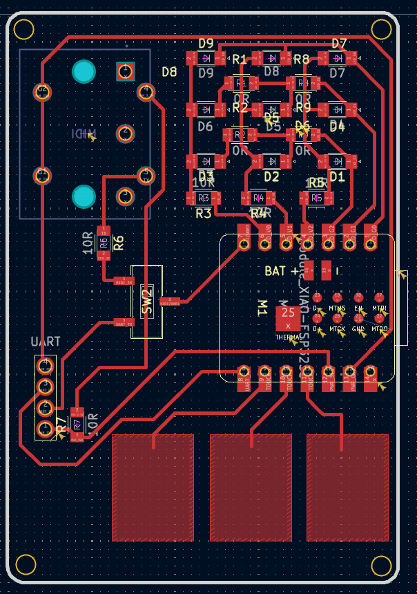
6.3.3.2. Traces
Before tracing, 2 things shoud be done:
Setting the Design-Rules for your production place in ‘Board Setup’
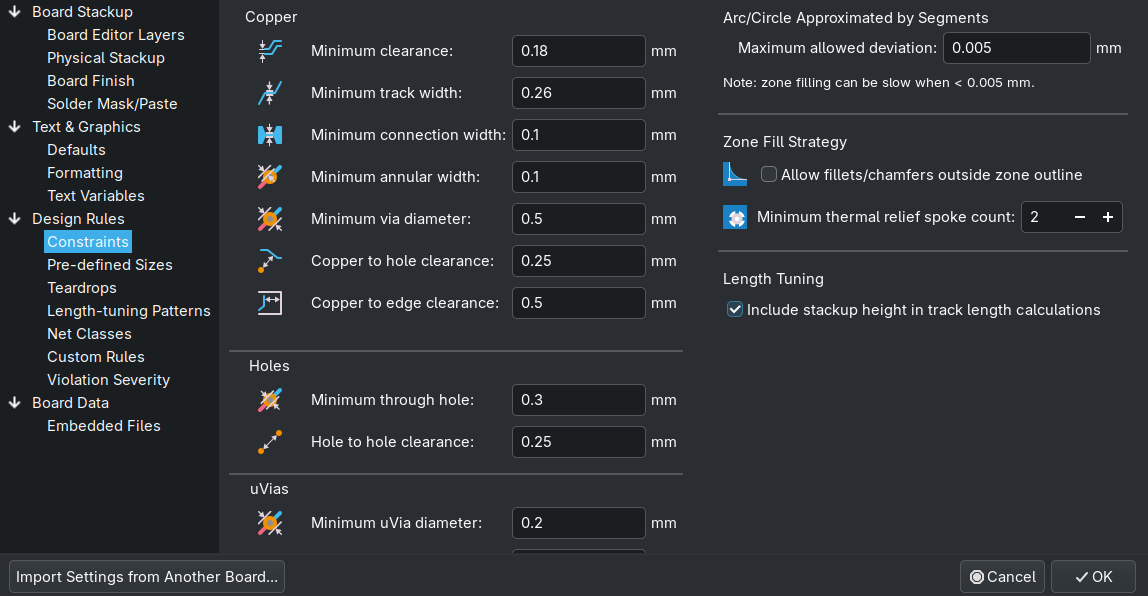
Decide for the default widths used for your traces, usually don’t use the smallest possible (try only when necessary), also in ‘Board Setup’
Also here, designing is pretty straight forward.
You import the components form the schematics ‘Update PCB from schematics’.
Then initialy place them and look for the ratsnest
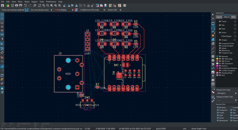
And then connect everything:
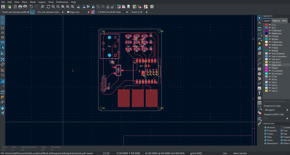
But there are still errors and I forgot the design rules for producing it.
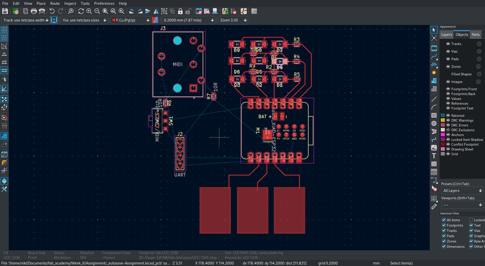
So I fixed it:
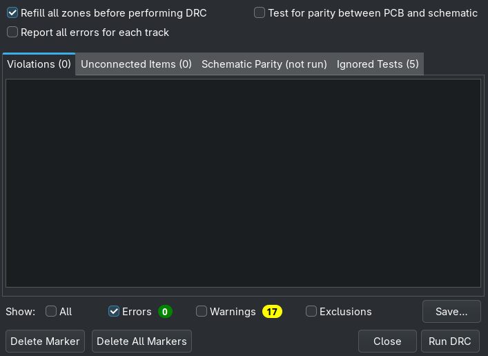
Outcome
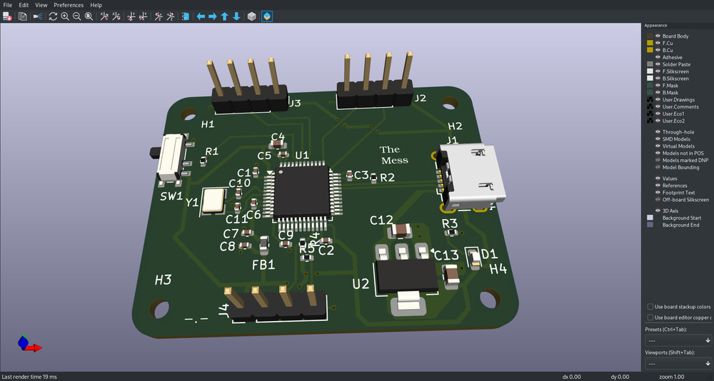
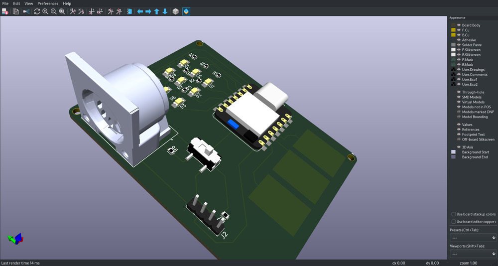
6.3.3.3. 3D Model
Outcome
6.3.3.4. Design Files
6.3.4. Verilog
Unfortunately I couldn’t find time to try it out but I really would love to, because I liked what Neil showed use the programming way :D