16. Wildcard Week - Week 16
16.1. Assignment
FPGA Programming
‘group assignment’
Find out and document the toolchain used for you FPGA chip
individual assignment
create a circuit/program on an FPGA
that interacts with an input/output device
simulate the program
For this assignment I have chosen to learn about the chip design and testing process with FPGAS, because it is a different process compared to electronics production and also embedded programming because of the process to connect the logical blocks.
16.2. ‘Group Assignment’
16.2.1. General
See also
German Repo with good materials and source information I used to get started.
Also a very good German CCC presentation.
From there I got all the explanations, images and code mentioned below.
FPGA (Field Programmable Gate Array)
IC with programmable logic after manufacturing
consists of array of programmable logic blocks with connecting grid
good for fast logical units with only one purpose, that may need to be configured/optimised after manufacturing and integrating it at an application
have high signal processing speed and parallel processing abilities
sequential logic: logic is only evaluated on clock
combinatory logic: immediate evaluation
General internal structure
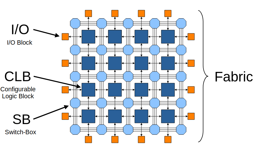
General simplified structure of the FPGA interconnect
I/O, CLB and SB are Configurable
(Source)
Configurable Logic Block (CLB)
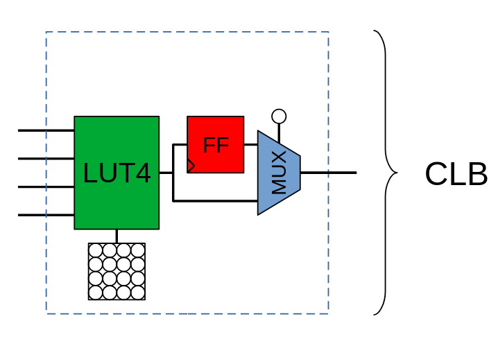
Configurable logic block conceptual
LUT - lookup table;
FF - flip-flop(‘>’ means CLOCK input);
MUX - Multiplexer
(Source)
LUT used for the logic to be used (AND, OR, XOR, …)
FF implements the sequential part for the logic
MUX for changing between combinatory and sequential logic
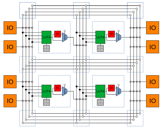
Configuring/Programming
Then to program it you connect the I/O Ports and the output of the CLBs to the bus and interconnect those appropriately.
E.g.:
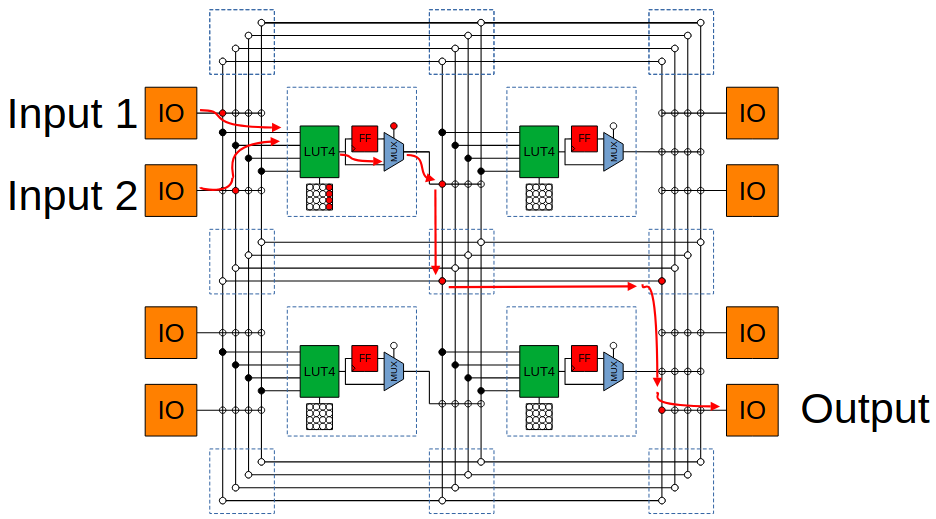
And this is programmed with a BITSTREAM containing those connections and settings (0 for not connected, 1 for connected)
e.g.:
# bitstream
...10000100...1000...10001000…
#                        ^^^^ .. SB5
#                    ^^^^ .. SB4
#             ^^^^ .. IO7
#      ^^^^ .. IO1
#  ^^^^ .. IO0

...0001000100010001...1...1000...
#                         ^^^^ .. OUT0
#                     ^ .. MUX0
#  ^^^^^^^^^^^^^^^^ .. LUT0
usage of an Hardware Description Language(HDL) or a schematic design to design and create the circuits
16.2.2. iCE40UP5K
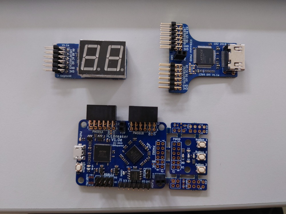
I’m going to use the open source iCEBreaker FPGA board based around the Lattice iCE40 UltraPlus 5K, which is nice for beginning because all open source tools are good integrated with this board.
Specs:
5280 Logic Cells (4-LUT + Carry + FF)
128 KBit Dual-Port Block RAM
1 MBit (128 KB) Single-Port RAM
PLL, Two SPI and two I2C hard IPs
Two internal oscillators (10 kHz and 48 MHz)
8 DSPs (16x16 multiply + 32 bit accumulate)
3x 24mA drive and 3x hard PWM IP
Tools:
iverilog - simulation of the bitstream
GTKWave - visualise the simulation
yosys - Synthesising tool to get the from RTL to GL
nextpnr - place and route, creating
icestorm - creating the bitstream for the iCE40
openFPGALoader - flashing tool to upload bitstream
Also cool:
16.2.3. Workflow
16.2.3.1. HDL (Hardware Description Language)
To easily create a bitstream and build complex circuits a common use is an HDL which is like a programming language but it describes the circuits, that should be created and connected.
And for those languages, there are 3 levels of abstractions
GL: Gate Level -> actual gates and connection of them (lowest level)
RTL: Register Transfer Level -> Working on registers and logic, that connects those registers, works on a clock cycle, used in HDL
Behavior level: Expected programm/hardware behavior (highest level)
The most common ones are Verilog and VHDL.
Here an example in Verilog:
// programs are structured in modules
// modules have input and output pins they use
module counter (
    input  clk,
    input  reset,
    output out
);

    // 8bit register
    logic [7:0] count;

    // implements a flip-flop
    // @ describes, when this block is evaluated
    // posedge: evaluate on positive edge (negedge==negative edge)
    always_ff @(posedge clk, negedge reset) begin
        // on reset edge
        if (!reset) begin
            count <= '0;
        // on clock edge
        end else begin
            count <= count + 1;
        end
    end

    // assign the last register value to the output pin
    assign out = count[7];

endmodule
Note
This ‘program’ above actually describes the hardware structure, not a sequential order of instructions, a processor evaluates ;>
This program implements a little counter, output the MSB.
16.2.3.2. Simulation and Waveform
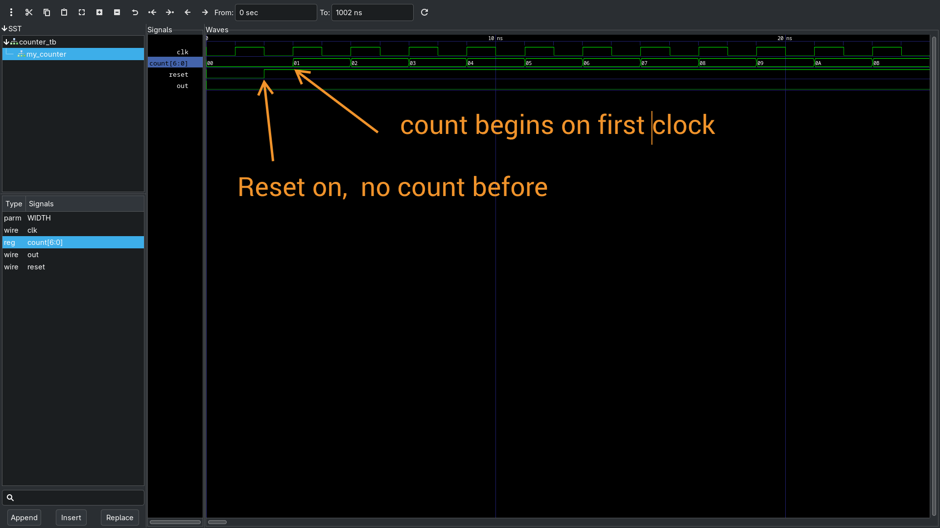
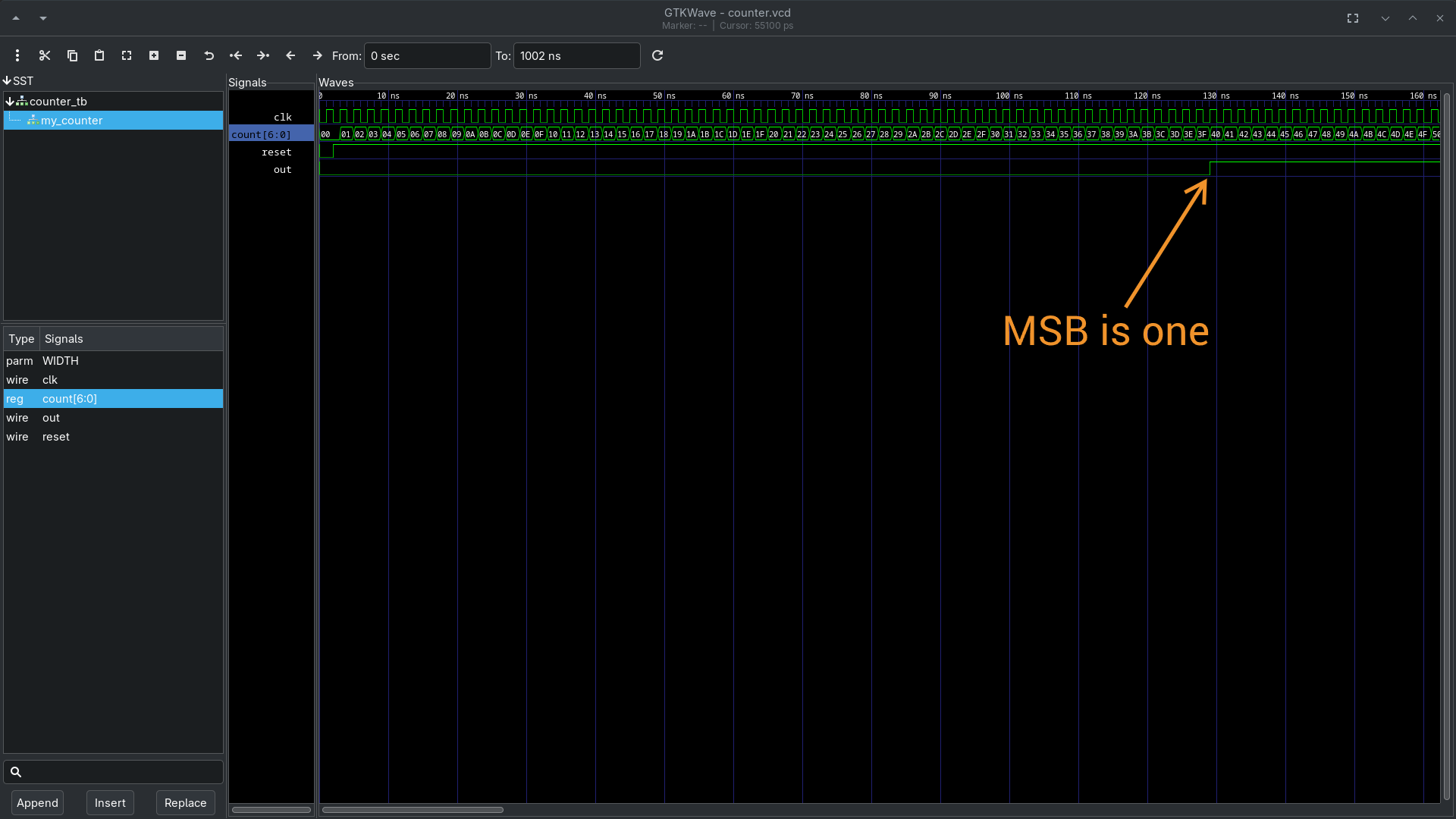
For a simulation, we need the code we want to test, a testbench, a simulator, which will be iverilog, and something to visualise the simulation, which will be GTKWave.
Testbench
A testbench is just another modules which generates a signal to test with and starts the program we want to test.
E.g.:
// a new module
module counter_tb ();


    // to signals, clock initially 0
    logic clk = 1'b0;
    logic reset;

    // always invert the clock on #1 period
    always #1 clk <= !clk;

    // only executed once
    initial begin
        $display("Simulation start!");
        reset = 1'b0; // Assert reset
        #2;
        reset = 1'b1; // Deassert reset
        // wait 100 cycles
        #100;
        $display("Simulation completed!");
        $finish;
    end

    // dumb all variables and output in a file
    initial begin
        $dumpfile("counter.vcd");
        $dumpvars(0, counter_tb);
    end

    // initialise the counter program
    counter my_counter (
        .clk    (clk  ), // connect clock with clock
        .reset  (reset), // and reset with reset
        .out    (     )  // does not need to be connected because you can see it in the dumb file
    );

endmodule
Simulation
# Create the simulation file
# -Wall: all Warnings
# -o: outputname
# -g2012: enable 2012 SystemVerilog support
# -s: top-level module
iverilog counter.sv counter_tb.sv -Wall -o counter.vvp -g2012 -s counter_tb

# Simulate
vvp counter.vvp

# view the simulation
gtkwave counter.vcd
16.2.3.3. Programming the Hardware
For programming, we need to:
‘Synthesise’ register abstractions to gate representation (RTL to GL)
Place and Route the single components available on the FPGA
Generate the bitstream for the FPGA
Upload the bitstream to:
RAM for only onetime execution or
FLASH to keep after power loss
For the Place and route we need constrains for the board we use, e.g. the IO numbers of the pins we use, the clock frequency, etc. Because we need to set the location of the Input/Output parts (parameters) in the code to the real hardware pins/devices.
So here we set the clock and IO pins of the buttons:
# 12 MHz clock
set_io -nowarn clk     35 # oscillator connect at this pin
set_frequency  clk     12

# LEDs and Button
set_io -nowarn reset   10 # Active low, Button
set_io -nowarn out     11 # Active low, LED
And then to the steps mentioned above:
# Synthesise the verilog code
# -p: call a specific script in yosys
# 'synth_ice40 -top counter -json counter.json':
#                   synth_ice40: call the synth_ice40 script
#                   -top counter: set the top modules as counter
#                   -json counter.json: output as json
# counter.sv: the design file
yosys -p 'synth_ice40 -top counter -json counter.json' counter.sv


# Perform place and route
# --json counter.json: input netlist from Yosys
# --up5k: set device type to iCE40UP5K
# --package sg48: set device package
# --asc counter.asc: asc bitstream file to write
# --pcf counter.pcf: PCF constraints file
nextpnr-ice40 --json counter.json \
    --up5k --package sg48 --asc counter.asc \
    --pcf counter.pcf \
# and to get an image representation of the routing
#   --routed-svg counter_placed.svg

# Convert to bitstream
# counter.asc: design input
# counter.bit: bitstream file
icepack counter.asc counter.bit

# Upload the bitstream to the board
# counter.bit: The bitstream to upload
# --board=ice40_generic: generic FTDI interface
# --write-flash: write bitstream in flash
openFPGALoader counter.bit --board=ice40_generic --write-flash
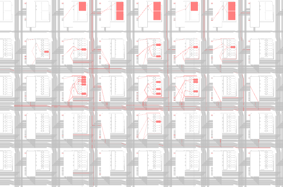
Routing
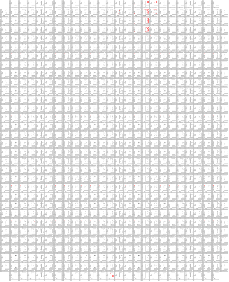
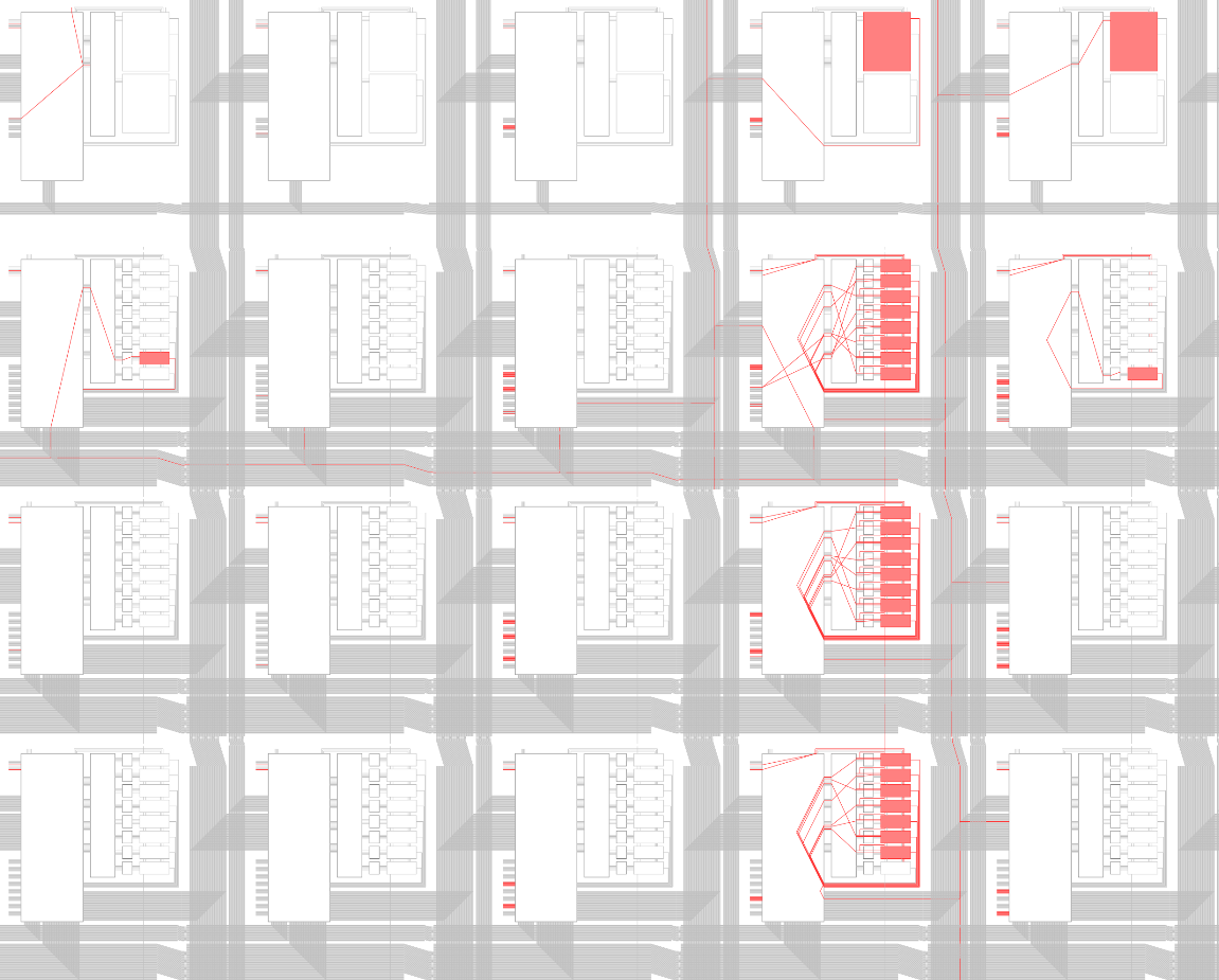
All
Zoomed In
Note
The number of bits in the variable counter was adjusted to 24bits so the LED would not blink that fast.
16.3. Individual Assignment
For the Individual Assignment I wanted to get the 7 segment display working.
For getting this to work I first looked up the pinout (full res image) of the icebreaker board and also looked into the schematics of the display:
There I’ve chosen the PMOD1A slot:
Next I installed all needed tools:
# packet manager for ArchLinux
sudo pacman -S iverilog gtkwave yosys openfpgaloader

# the other packages where not packaged for my OS currently so I used a nix-shell, where they are allready packaged and I didn't need to build them myself
nix-shell -p icestorm nextpnr
Then I programmed the Verilog code:
// define input and output pins for display, buttons and clock
module counter (
    input  clk,
    input  reset,
    input  up,
    input  down,
    output out,
    output outAA,
    output outAB,
    output outAC,
    output outAD,
    output outAE,
    output outAF,
    output outAG,
    output outCA
);

    reg [3:0] count;
    reg [7:0] outp;
    logic CA;

    initial begin
      outp = 8'd0;
      CA = 1'b0;
    end


    // count up when the up button is pressed
    always_ff @(negedge up) begin
      if (!up) begin
        count = count + 1;
      end
    end

    // change the digit on the 7 segment display when
    // the down key is pressed
    always_ff @(negedge down) begin
      if (!down) begin
        CA = CA+1;
      end
    end

    // always on clock update the value on count with the display
    always_ff @(posedge clk) begin
          case(count)
            // hardcode the numbers to the binary representation
            // of the 7 segment display
            //                ABCDEFG
            8'd0: outp <= 8'b00000001;
            8'd1: outp <= 8'b01001111;
            8'd2: outp <= 8'b00010010;
            8'd3: outp <= 8'b00000110;
            8'd4: outp <= 8'b01001100;
            8'd5: outp <= 8'b00100100;
            8'd6: outp <= 8'b00100000;
            8'd7: outp <= 8'b00001111;
            8'd8: outp <= 8'b00000000;
            8'd9: outp <= 8'b00000100;
            default: outp <= 8'b00000001;
          endcase
    end

    // assign the pins for the display with the output
    assign out = count[3];
    assign outAA = outp[6];
    assign outAB = outp[5];
    assign outAC = outp[4];
    assign outAD = outp[3];
    assign outAE = outp[2];
    assign outAF = outp[1];
    assign outAG = outp[0];
    assign outCA = CA;

endmodule
Now I wrote a little test bench to count to 3:
`timescale 1ns/1ps

module counter_tb ();

    logic clk = 1'b0;
    logic reset;
    logic up;
    logic down;

    always #1 clk <= !clk;

    initial begin
        $display("Simulation start!");
        reset = 1'b0; // Assert reset
        up = 1'b0;
        down = 1'b0;
        #2;
        reset = 1'b1; // Deassert reset
        up = 1'b1;  // count 1
        #6;
        up = 1'b0;
        #10;
        up = 1'b1;  // count 2
        #14;
        up = 1'b0;
        #18;
        up = 1'b1; // count 3
        #22;
        up = 1'b0;
        #26;
        down = 1'b1;

        #1000;
        $display("Simulation completed!");
        $finish;
    end

    initial begin
        $dumpfile("counter.vcd");
        $dumpvars(0, counter_tb);
    end

    counter my_counter (
        .clk    (clk  ),
        .reset  (reset),
        .up     (up  ),
        .down  (down),
        .out    (     ),
        .outAA ( ),
        .outAB ( ),
        .outAC ( ),
        .outAD ( ),
        .outAE ( ),
        .outAF ( ),
        .outAG ( ),
        .outCA ( )
    );

endmodule
Then I simulated it and looked at the Waveform:
As you can see, you see nothing. I couldn’t managed to get the simulation working…
But I thought I still give it a try.
Here the visualisation of the routing:
Then I flashed it to the FPGA and it actually works :D
Maybe something with my test bench is wrong but it works on the hardware, so good enough ;]
Note
Getting the code to compile and to understand, why yosys won’t ‘compile’ is not that intuitive and even harder than debugging SEGFAULTs in C and C++ -.- But I managed to debug it and I found out, that yosys can’t actually resolve every syntactically correct construction, because:
Its dependent (and also describing hardware), meaning if the hardware does not has some capabilities/components needed to build a yosys resolution, than it obviously fails (because yosys makes many checks after it build the GL abstraction)
It actually can’t solve some constructions yet ._.
See also
fpgatutorial - tutorials to get started with SystemVerilog