Design
Most of the time I work on the design of the mechanics so they work properly.
I made everything in FreeCAD and KiCAD.
In FreeCAD I also made many thing parametric on one hand for easier adjustment and possible errors in production/assembly.
Electronics
For the electronics I separated the project into 5 different modules for easier replacement, if some get destroyed while using (because some of them are mechanically stressed on usage, see below).
Schematics
I used 2 ATtiny because I did not had enough input pins on the ATtiny1624 either and I wanted to be decoupled from the top MIDI module to easily replace and extend it on that part (and I missed, that we had an ATtiny in the inventory with more pins (ATtiny3226) -.- )
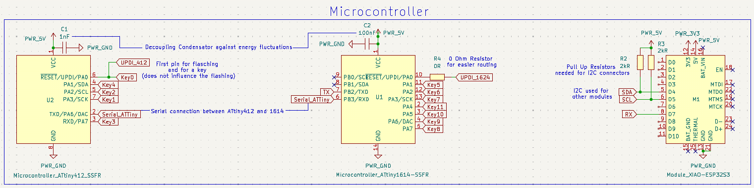
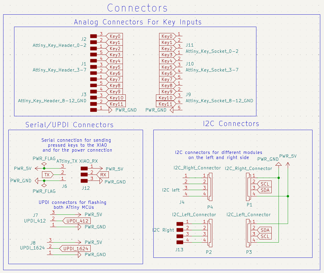
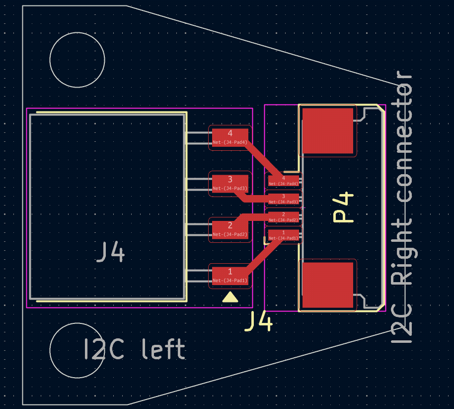
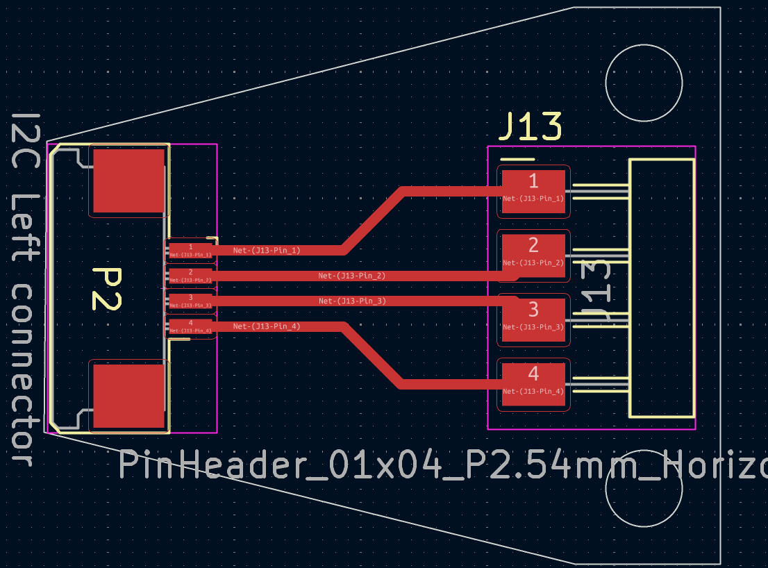
For the connectors I used simple pin header and for the I2C because I wanted to make extra PCB for them I used cable connectors for it (and I didn’t want to make a big PCB because this would be a part that could break easier).
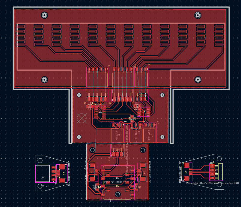
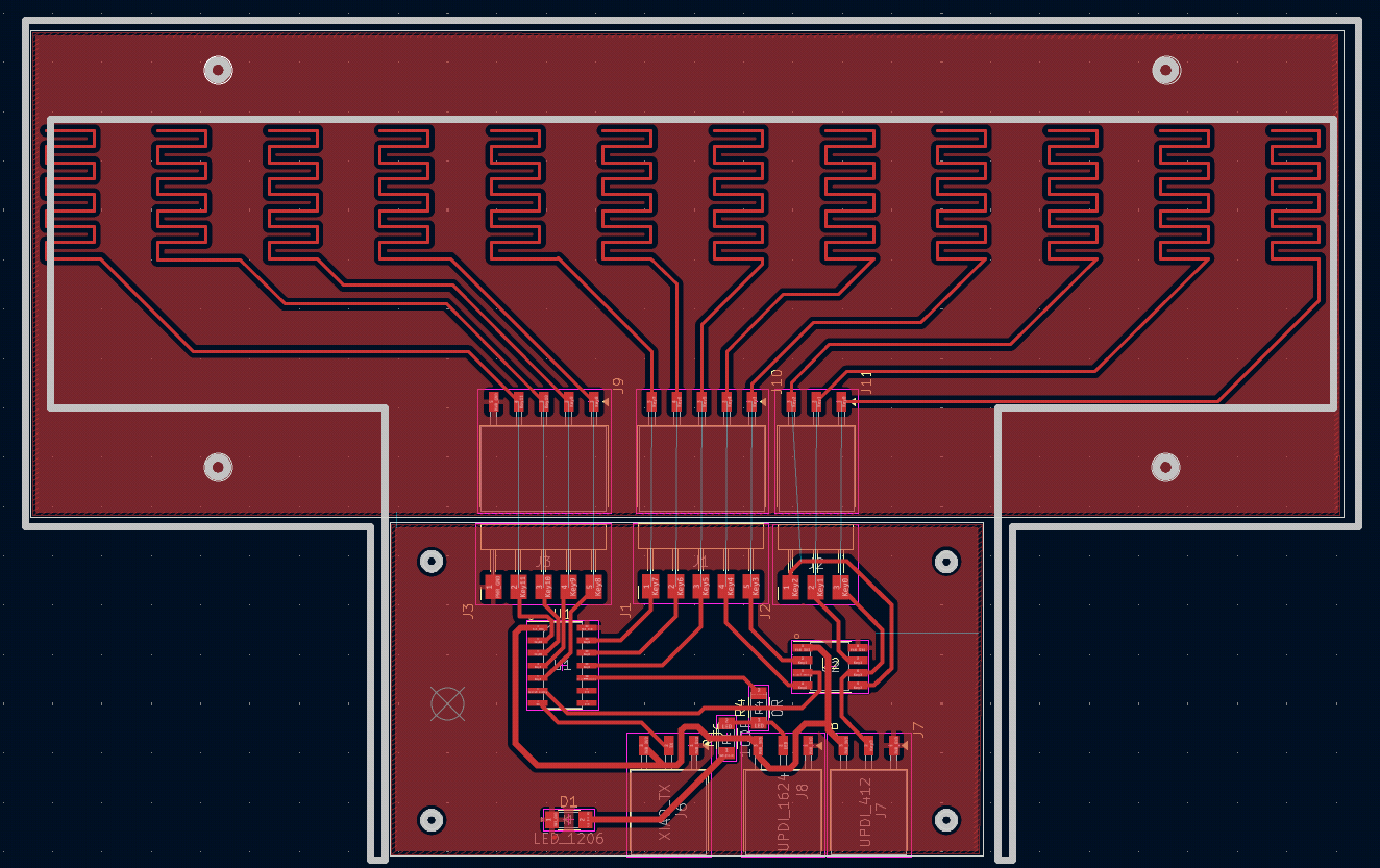
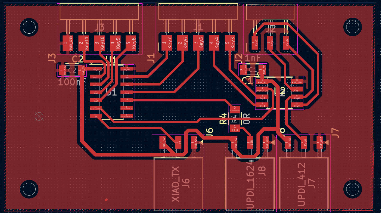
Routing
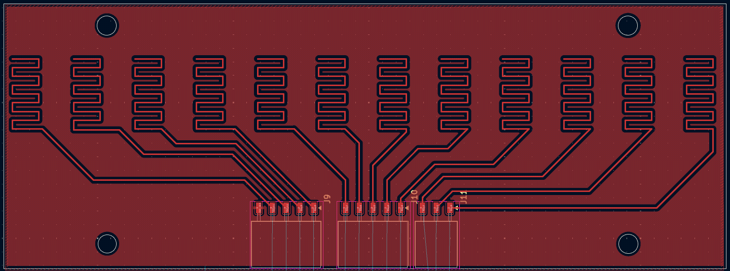
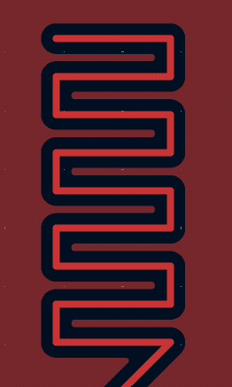
For the key traces I simply used a ground-plane and a windy, square-wave like structure that gets connected with the conductive foam when touched.
I used small traces and many winds to increase the probability of connecting the ground plane with the pin wire.
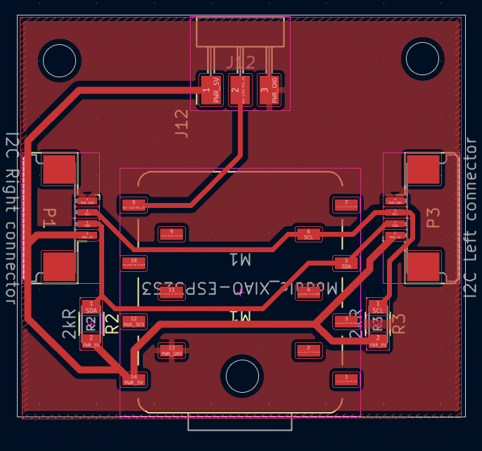
The ATtiny PCB is pretty normal except I adjusted the top left footprint for the 3 pin header so the ground plane can fit through the soldering pads.
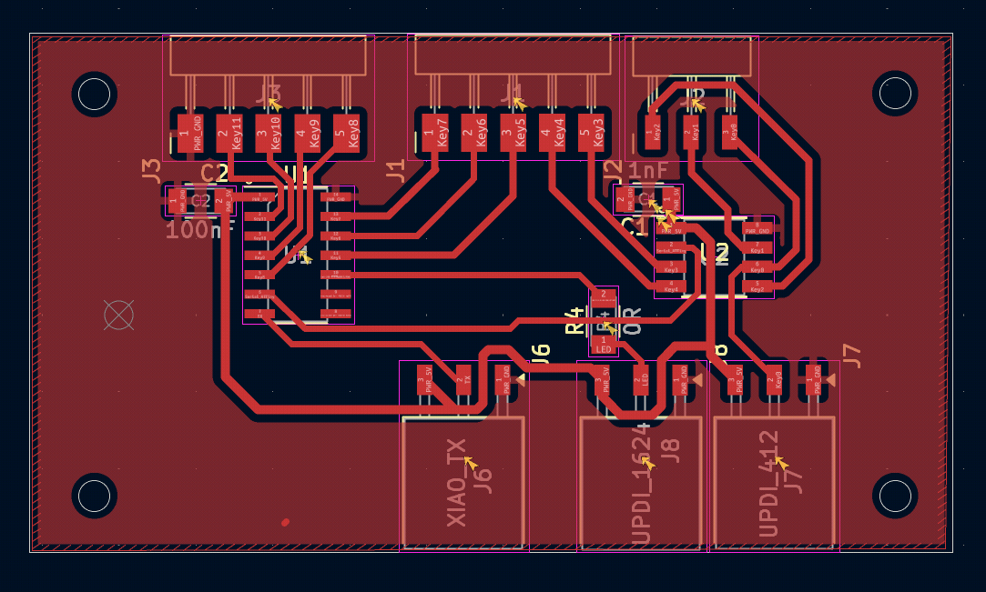
Also I only noticed now, that the decoupling capacitor could have been placed nearer to the VCC and GND pins as mentioned here. But this was no problem in the end.\
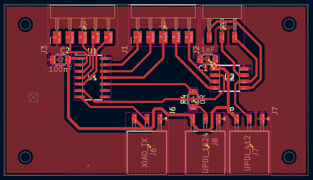
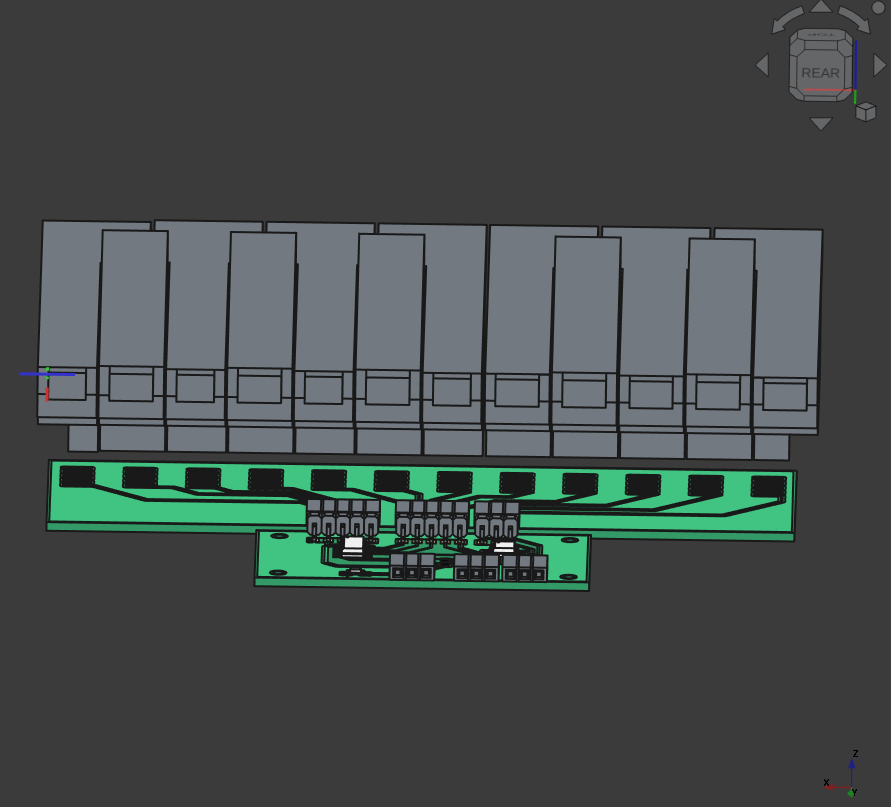
And here the PCB with the XIAO and the I2C connectors for the other modules on the left and right side.
System Integration
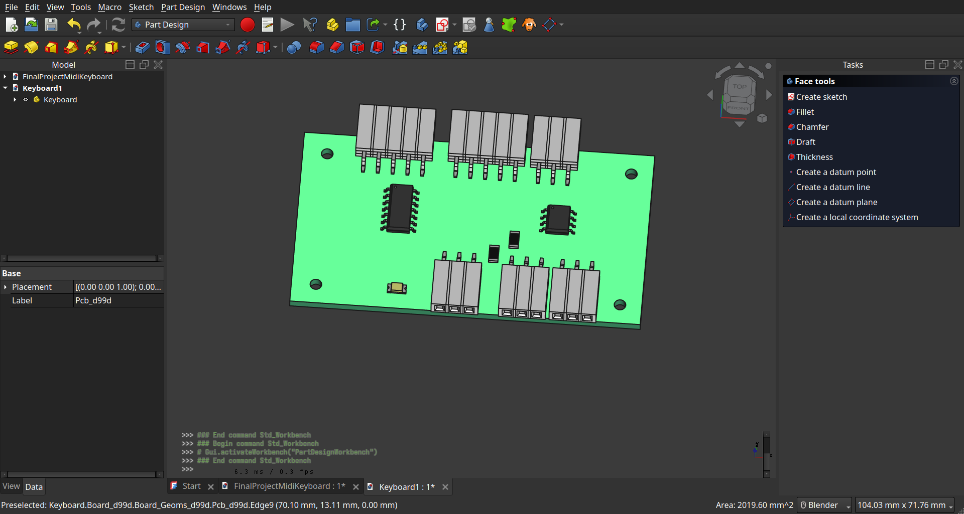
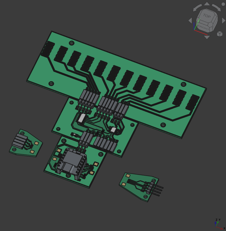
For system integration I designed the PCBs in one file and aligned the header here so they should fit.
 For creating the edge-cuts and holes I used a sketch from the 3D modelling to adjust and create the holes in the PCBs.
Also I imported the PCBs into FreeCAD with the KiCADStepUp-Addon and then used those PCBs for further modelling.
Here I used shape-binders to base my modelling on it and also check in the assembly, if everything fits nicely with a bit of tolerance (see below).
And Because I had problems that when connecting the PCBs the peeled off from the PCB I made the traces a bit thicker (I don’t know, if this helped anyway ._.).
Before
After (look on the top pin header)
For more system integration, see below
Mechanics and Housing
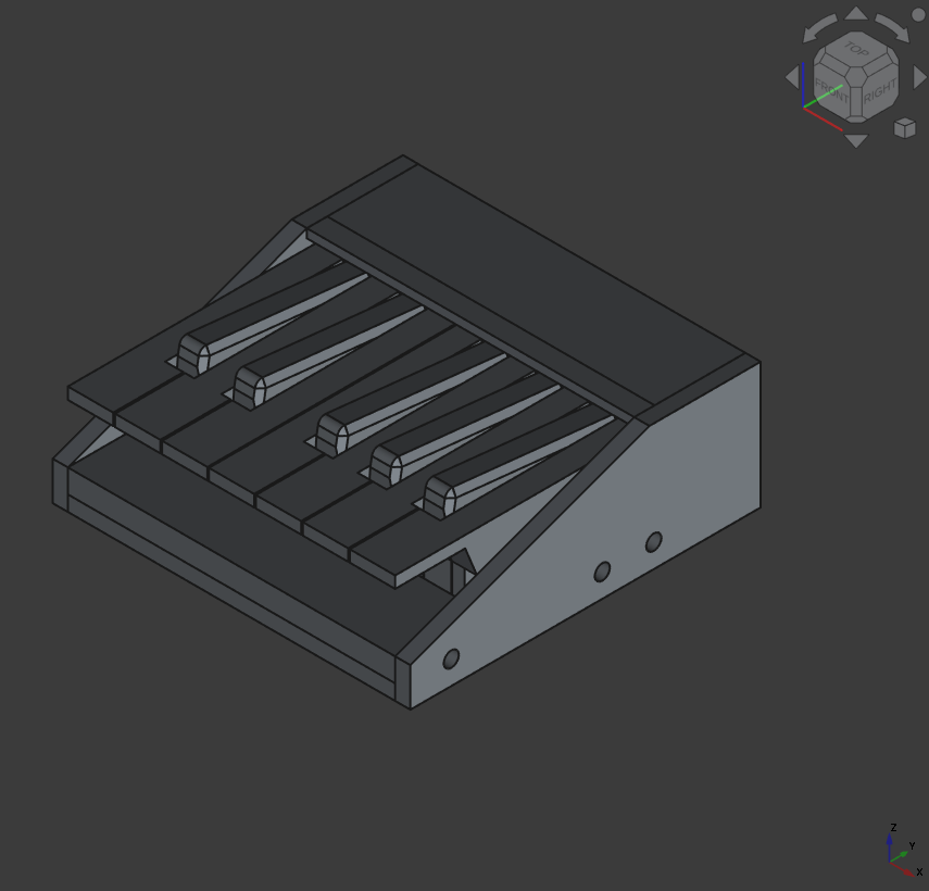
I started designing of the keys and housing and also tested the first assembly in the CAD-Week.
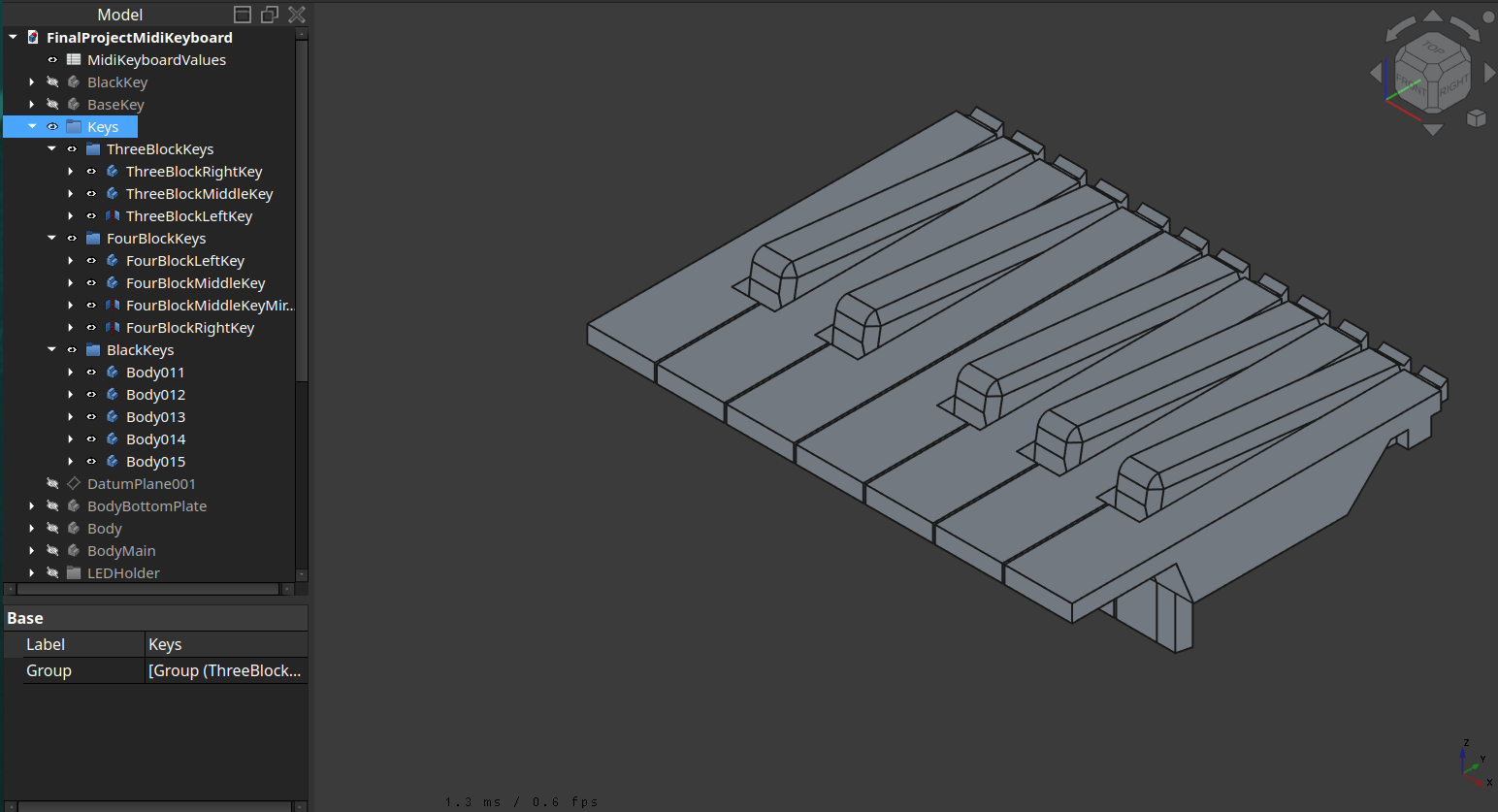
Keys
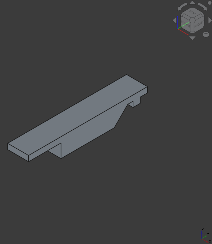
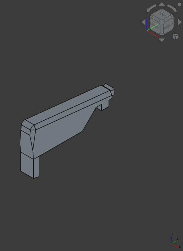
First I designed a base key which I used for the other keys to build upon.
I cut them by a specific calculation so the distance on the back is equal (almost ._.)
Housing
I also designed simultaneously the housing and for making better adjustment, I cut it up in 4 pieces:
 First Housing design
 Cut up in bottom plates, Led housing and key holder
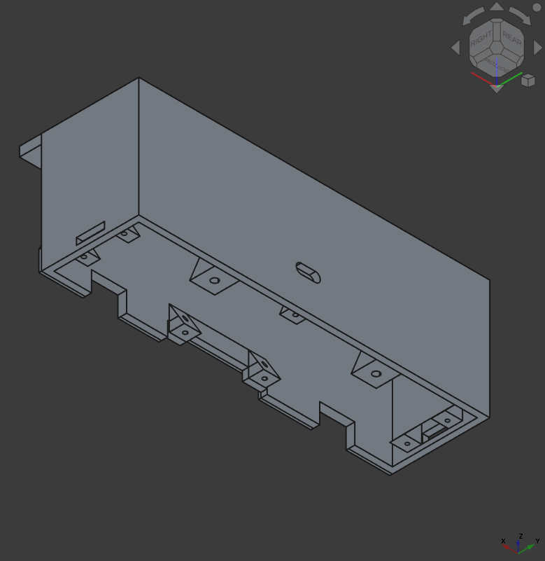
Key Holder
The I first extended the key holder design:
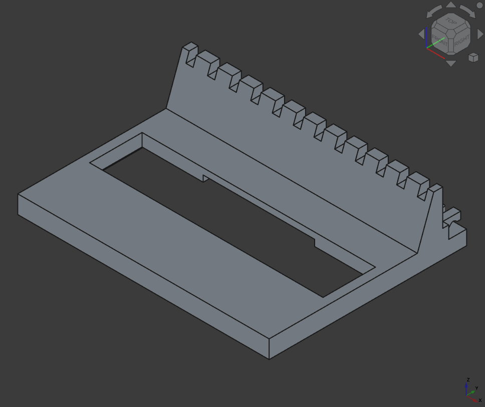 Here the harder part was the calculation for the right linear pattern I used for the key slots.
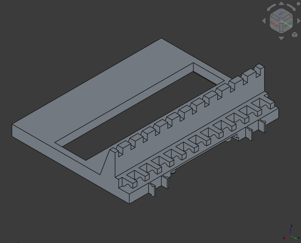 I also integrated snap-fits for the top modules and a b-spline structure for easier sliding in the rubber bands
 And then for a good system integration I added holes for the bottom plate, PCB and holes to but the magnets (slits on the side)
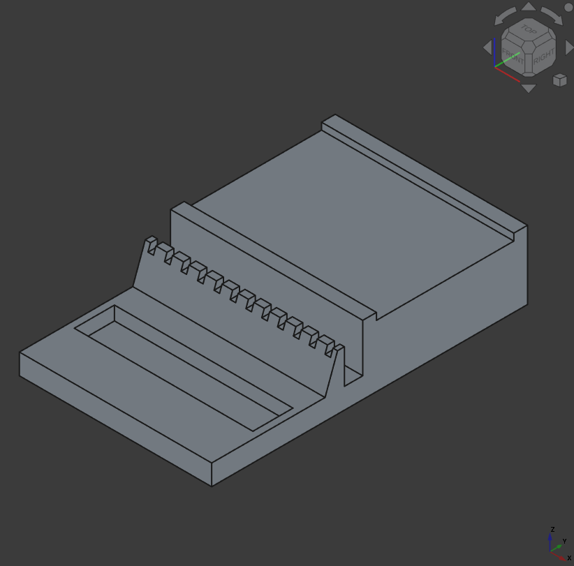
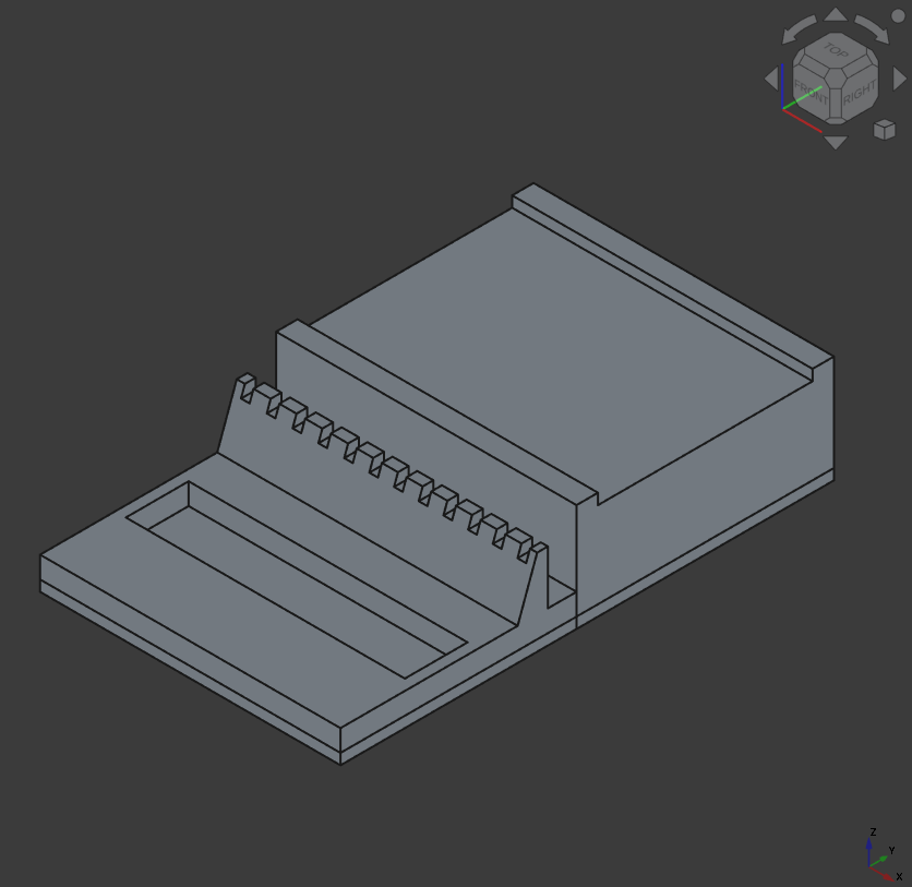
XIAO Body
Then I designed the first body for just the XIAO and the side connectors.
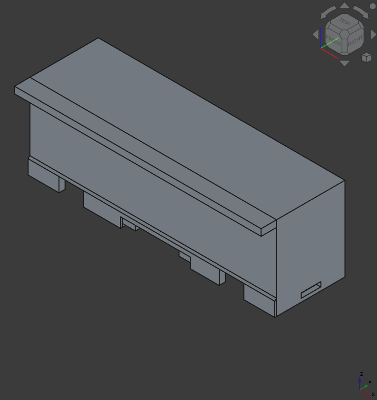
I made a little overhang for a better packaging (so you don’t see the rubber bands). Also note the slots on the bottom for the PCB and the snap-fits. And on the side for the modules.
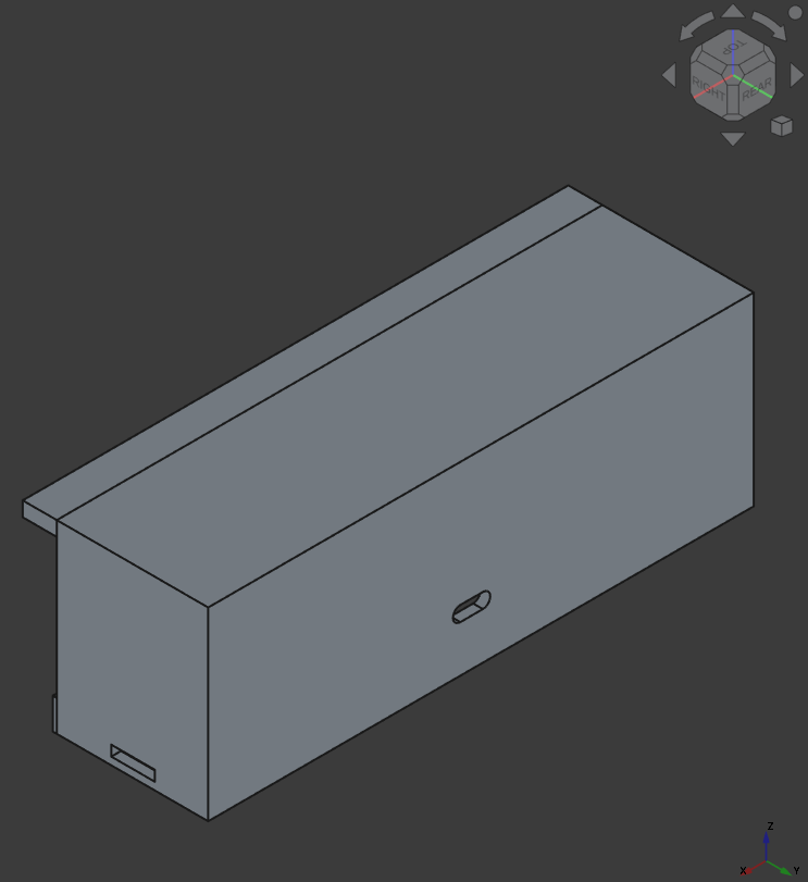
Also a slot for the USB-C connector, so that it lays inside the slot (see system integration).
And created inside the housing mounting holes for each PCB (the smaller ones) and for the bottom plate (the bigger ones).
Covers
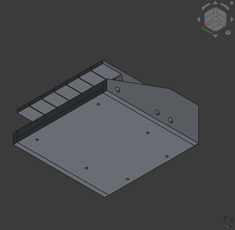
Next I designed a side and bottom plate to connect and cover up everything.
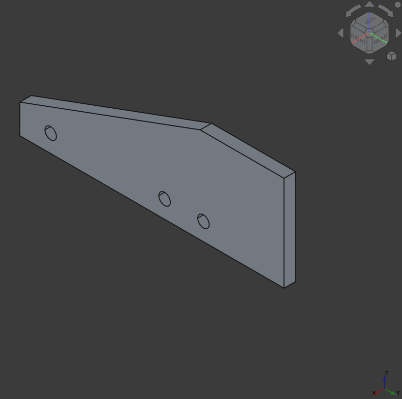 Side plate with holes for the magnets.
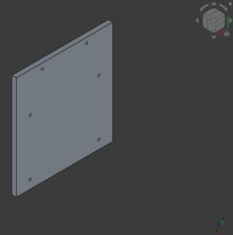 Bottom plate with holes for the screws
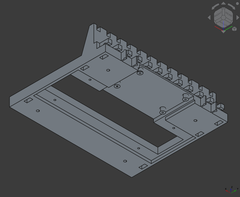
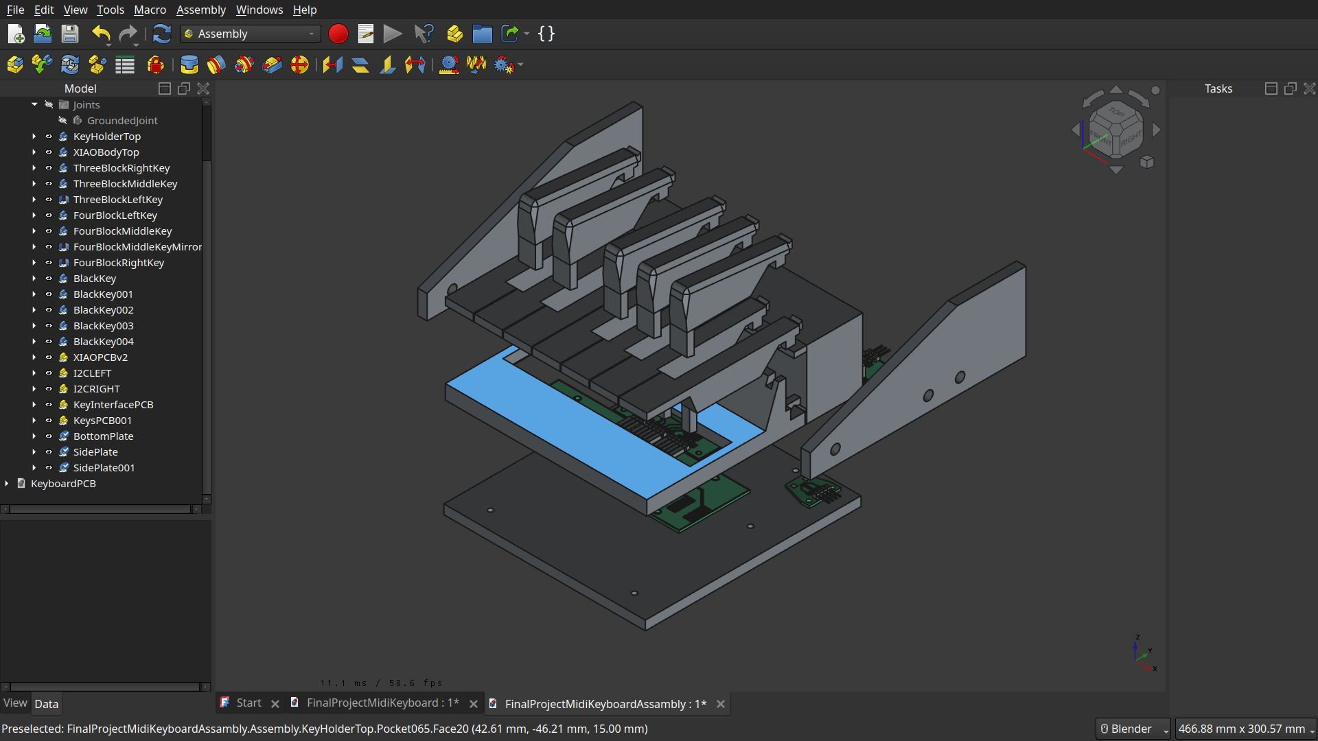
Assembly
Then I constantly worked with the assembly and tested everything there first.
Inside
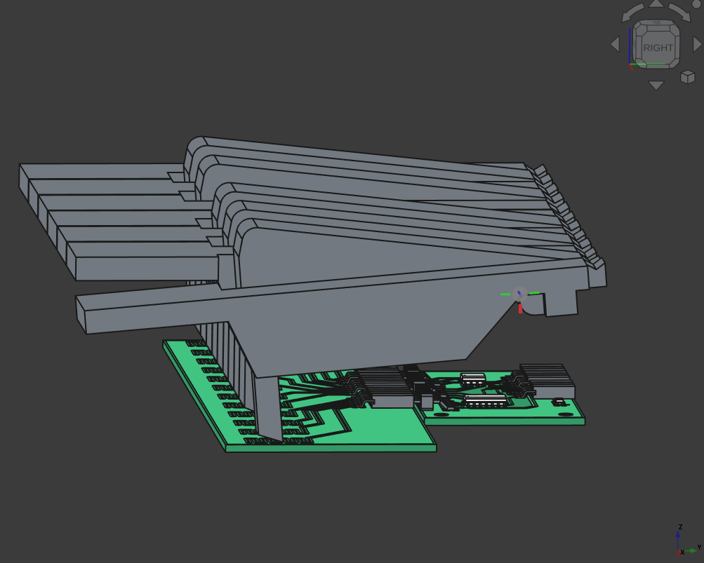
I tested the imported PCBs
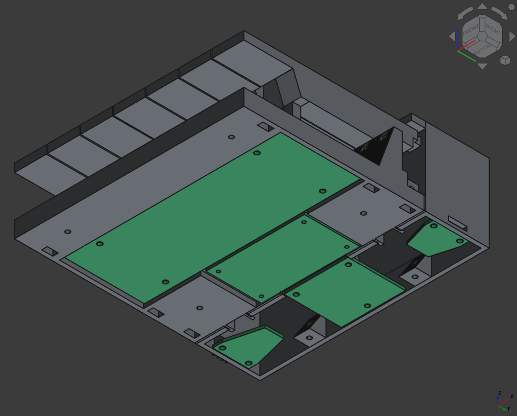
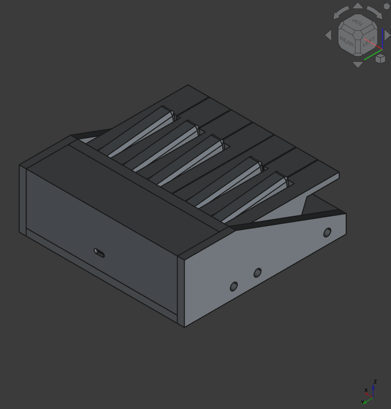
Assembled
Here the full assembly with the side plates.
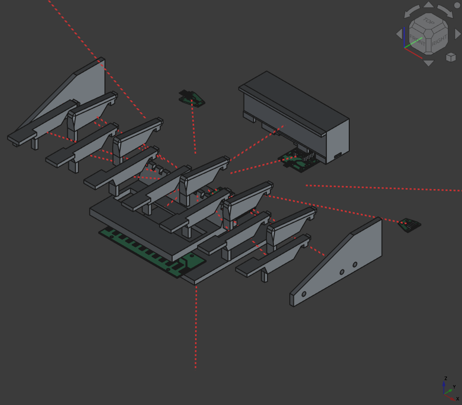
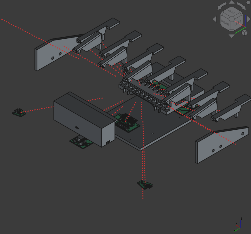
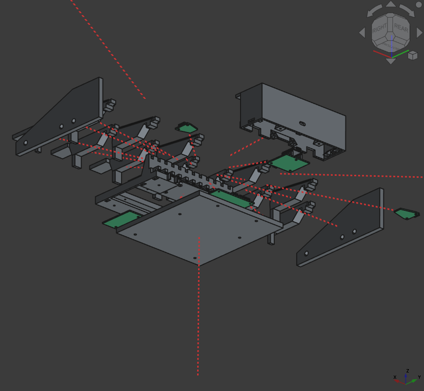
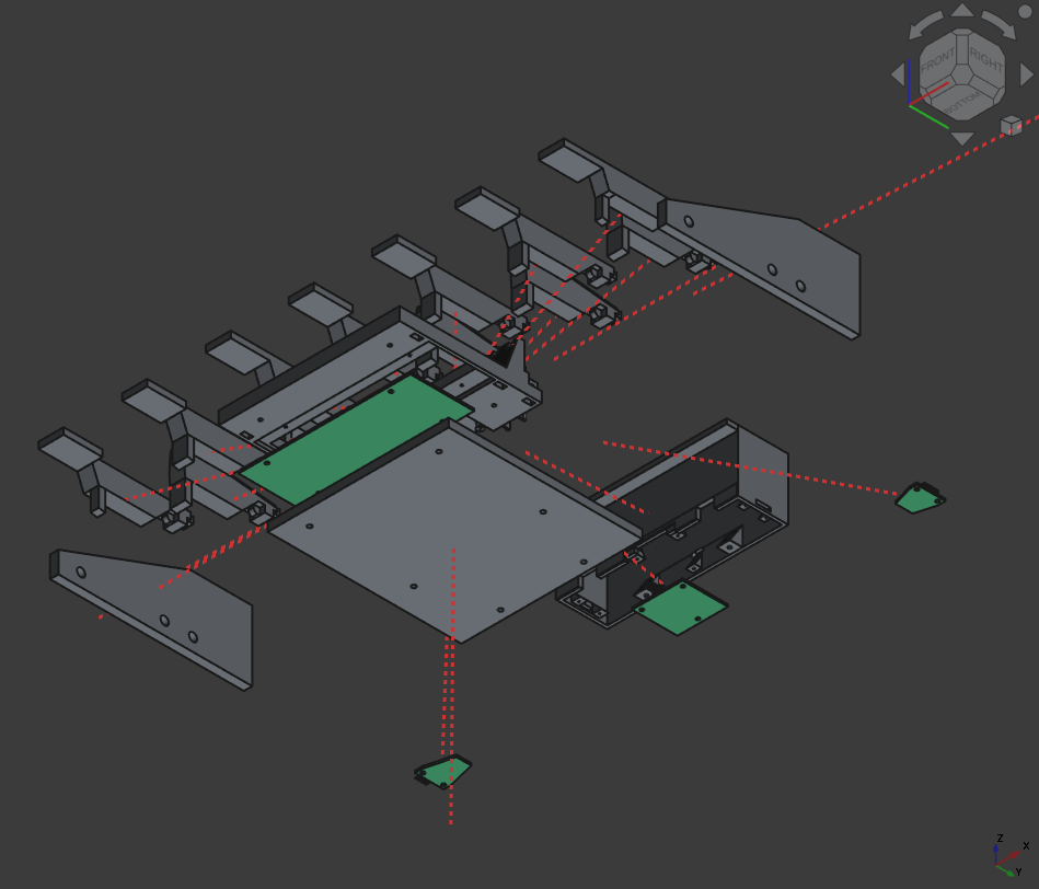
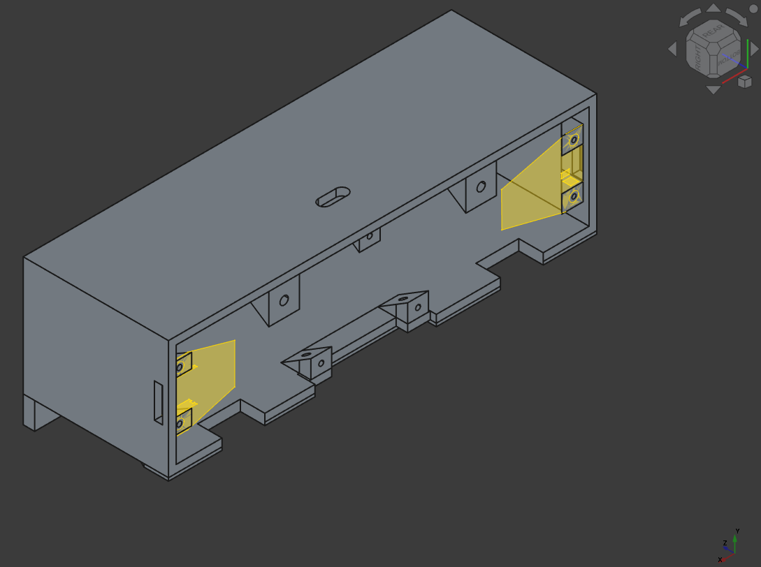
Exploded
And also here some exploded views:
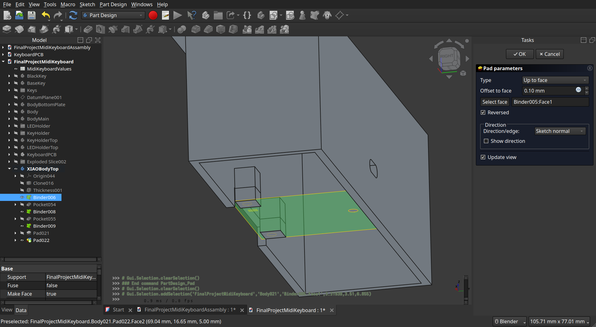
System Integration
To have a well integrated/packaged system I always tried to use the imported PCBs and the assembly as a reference to create the models.
 Here most of the time I used shape-binders from the assembly to create holes and attachment to the body on those shape-binders geometry.
This way (and with some tolerance) I could design very closely to the PCBs and could make a good and tight fit to them.
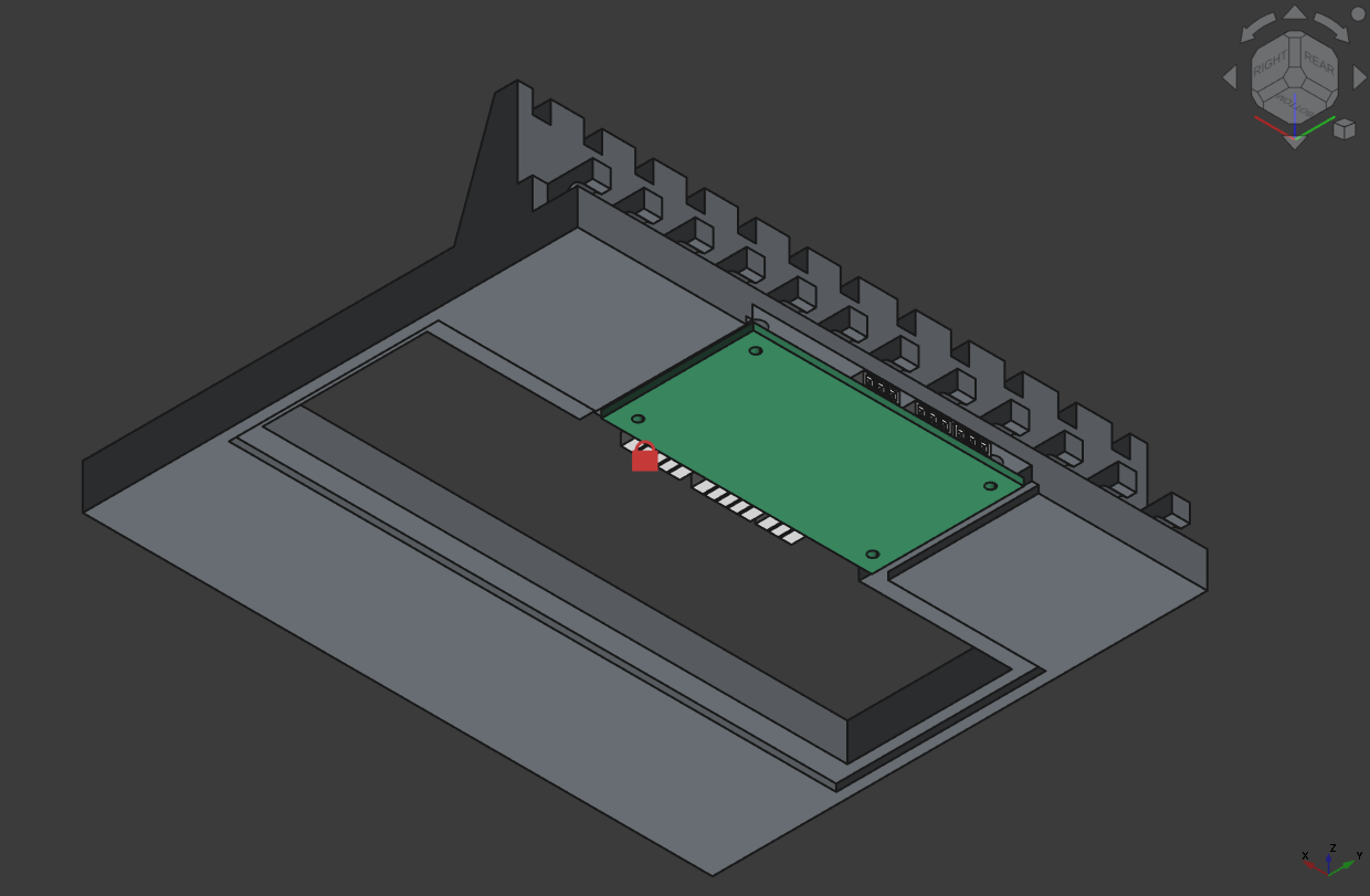
Here I checked the distance because we had only 25mm cable for the connector PCBs
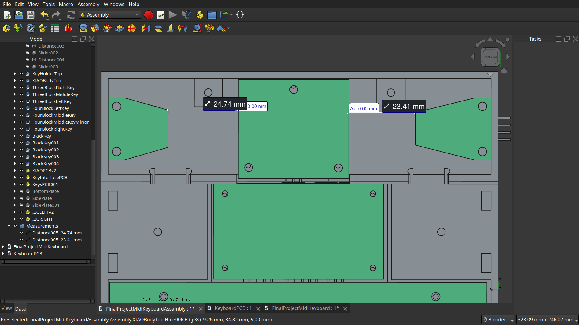
And here I used the assembly with a ‘Revolute’-Joint to test the keys on the PCBs:
 Here I tested the alignment of the individual keys so they hit the prepared traces.
 Here I tested the angle of the little cut when the key is pressed.
For the physical testing of the system integration, see here.