8. Electronics Production - Week 8
8.1. Assignments
Electronics Production
group assignment
characterize the design rules for your in-house PCB production process
individual assignment
make and test a microcontroller development board that you designed
extra credit: make it with another process
8.2. Group Assignment
8.2.1. General PCB-milling
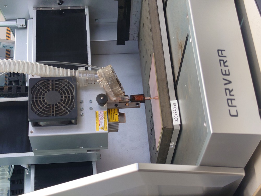
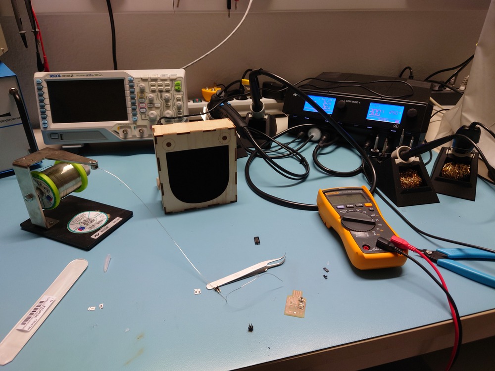
We used the Marcera Carvera for milling the PCB, which is very convenient because of the automatic tool changer.
8.2.1.1. Preparation
For preparation, we did the following steps:
(-1. HOME THE CARVERA)
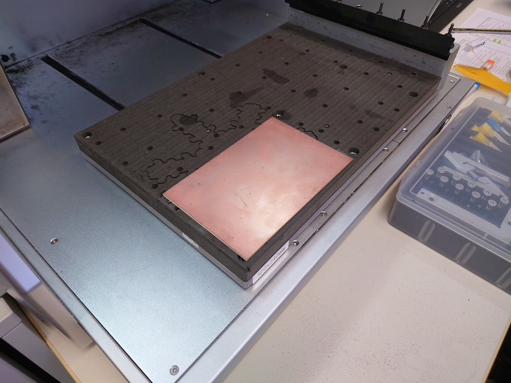
We milled our bed flat so that the PCB is exactly flat on the surface
We first check, if the board is straight (with a straight object, here a caliper):
if not, we just bend it, until its straight
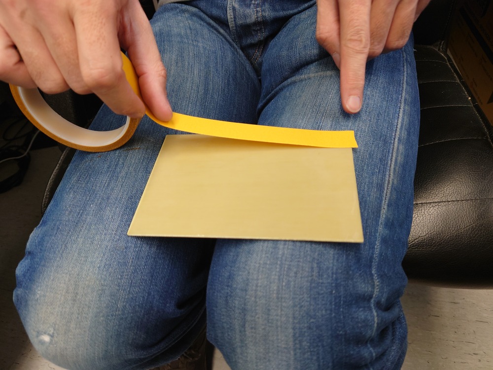
Next, we stuck double-sided tape onto our PCB and the PCB on our milling bed. Important here is:
The tape should have: thin adhesive, not to strong, no strings/structure strengthener in it and on the side
let edges of tape over PCB
look for dirt etc.
don’t need to tape everywhere
press down!
should not move
Another very important step is the exact Z-Zero point, which should be on top of the PCB with a high accuracy.
to deep -> mill might break (especially normal, thin mills, v-bit is fine)
to shallow -> path with not wide enough
Approaches:
Use the auto-z-probe of the carvera, but this is not very precise und thus unsuitable
Drop the tool, drive down and grab it again, but this approach also does not work that nice with de Carvera, because of the rubber stopper
Use a multi-meter, spin the mill and touch mill and board with the multi-meter and drive down, until it beeps
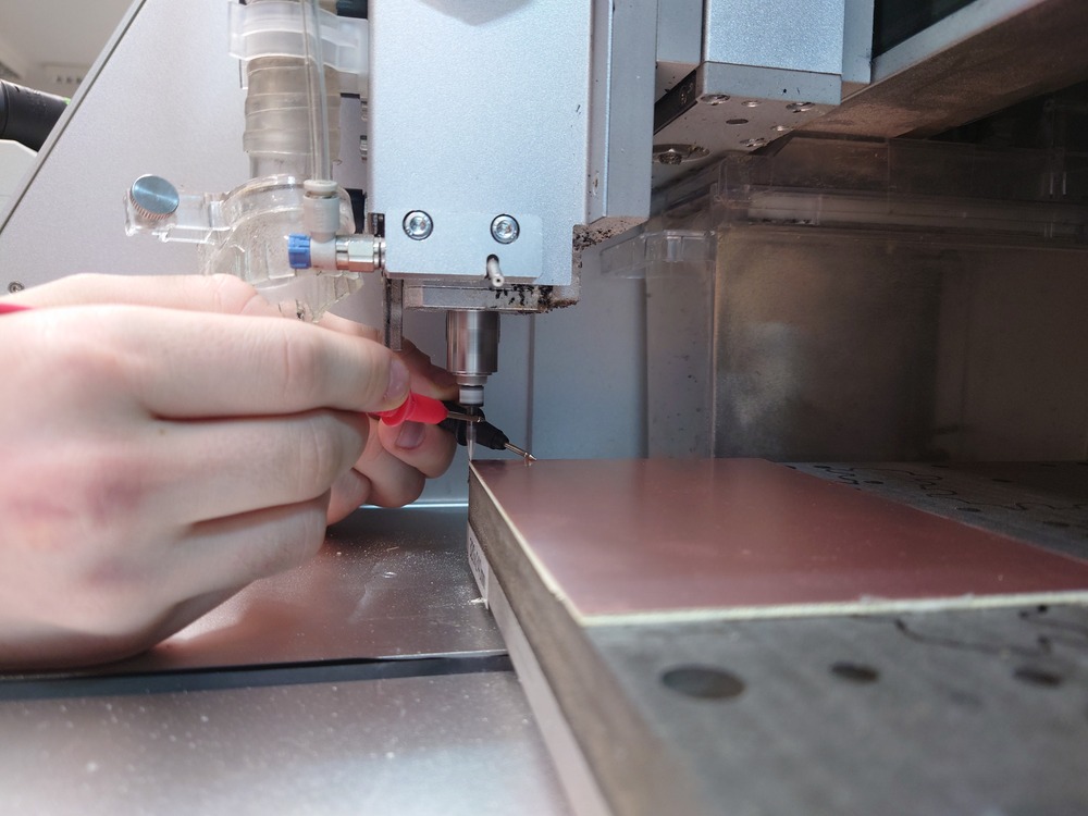
We have chosen the 3. Method, which resulted in a good z-zeroing.
Now just setting the x and y work origin and milling could start.
8.2.1.2. GCODE-Generation
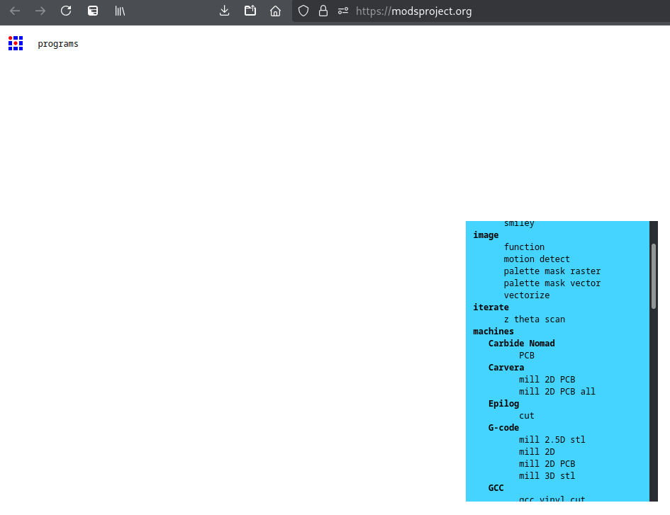
For generating the GCODE, we use the Fabmodules (Source-Code) with the already prepared Carvera-Program.
How It Works
The Fabmodules use a black and white PNG file and look for edges from white to black, meaning that the path to carve out should be white.
It just goes through the PNG line by line and calculates the distance to those black and white differences and saves the shortest one in a matrix. And this is done from every direction and reverse. This results in a big matrix where 0 means there is a trace and a bigger number means there is no trace.
Then to generate the path, it uses on one hand the tool diameter and the offset-number to generate the path.
Pretty cool and easy principle :D
Generation
So the workflow breaks down to those steps, when the pcb is designed in :
Generate the black and white PNG of the traces and exterior
more notes on those step is below, because its not trivial/easy (as I hoped)
Go to the Fabmodules and open the Carvera-Program (right-click->open program->carvera->mill 2D PCB) Also in the prepared program, an exterior can be chosen simultaneously to do the path-carving and cutout in one go. The ‘mill 2D PCB all’ program is used for removing all of the copper from the PCB.
On the left modules, ‘Select PNG file’ and upload on the top the pathes and on the bottom the exterior cutout.
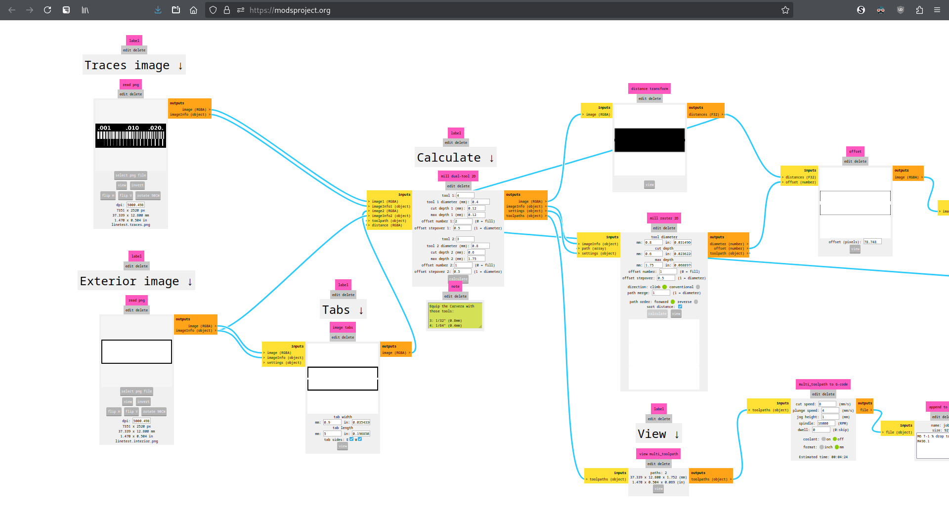
Next set your mill and PCB parameters on the middle ‘mill dual tool’-module (especially the tool diameter and cut-depth and max-depth) and machine-speeds on the ‘multi_toolpath to gcode’-module (maybe cut- and plunge-speed and spindel RPM).
we just changed:
first tool diameter: 0.2mm
cut depth: 0.3mm
cut max: 1.6mm
and reduced cut speed to 6mm/s and plunge-speed to 3mm/s
also in later setting we used for ‘offset-number’ 4, which resulted in better separated paths (from the rest-copper)
Then click ‘Calculate’ on the middle module to generate the gcode, you can then save the .nc file and look at the GCODE on a little preview (if it does not pop up, use ‘view multitool_path ‘ module)
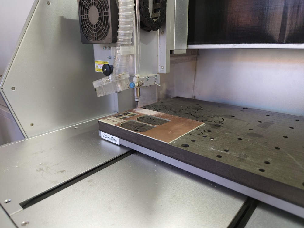
8.2.1.3. Milling
In Preparation we already setup the Carvera.
So we just need to upload the GCODE tho the machine (bottom-left ‘page’-icon -> upload), select the file (in the view, click select), last time check the g-code in the preview and then start the milling (bottom left play-button).
Then use a scraper or knife to cut the taps and carefully break out the board from the rest. To clean up the traces, use the knife/scraper or steel wool to remove the ridge.
8.2.2. Design-Rule
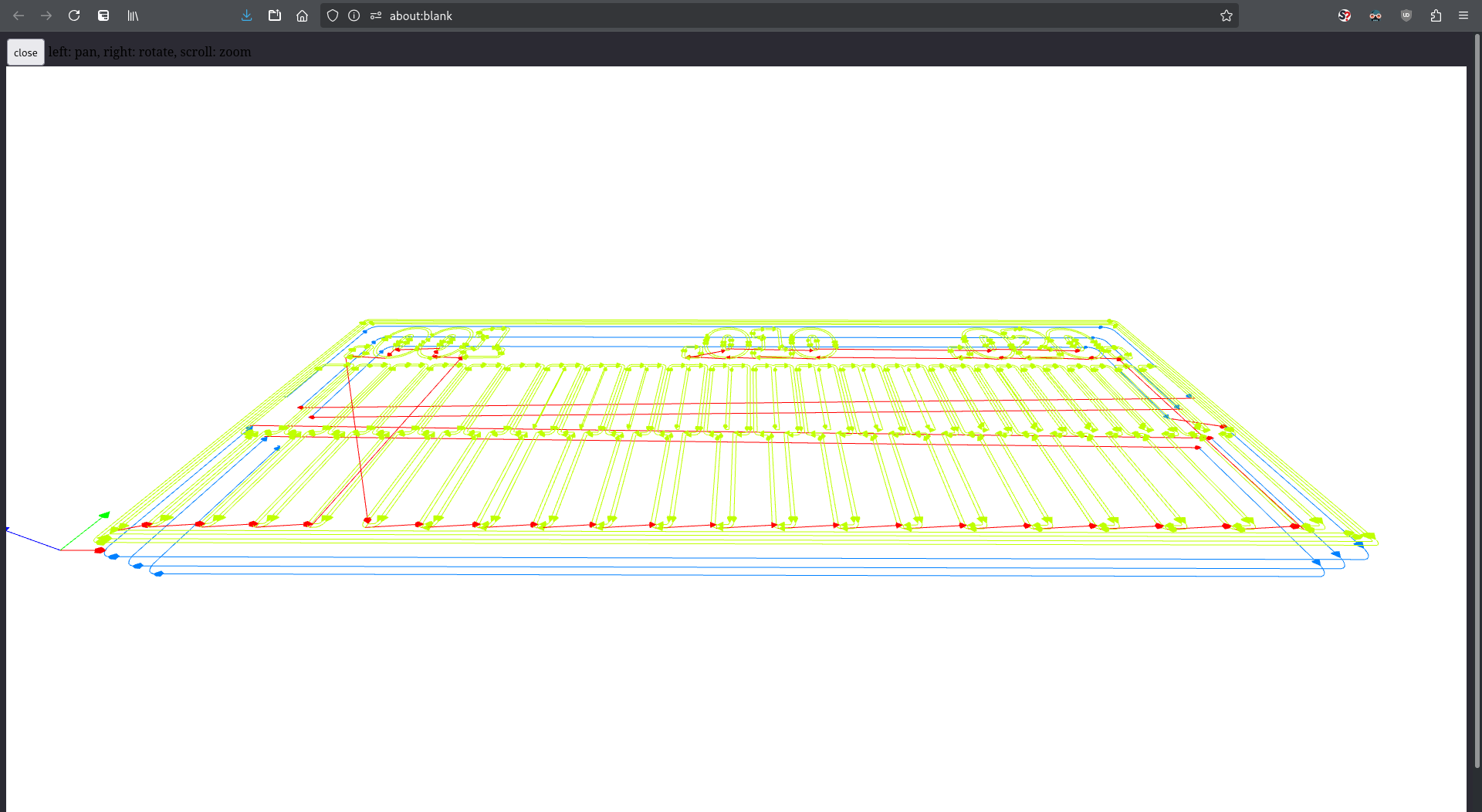
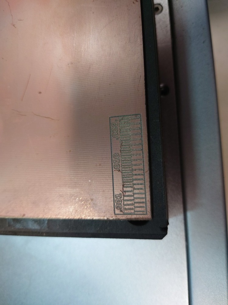
To determine the design-rules, we used Neil’s Traces-Test.
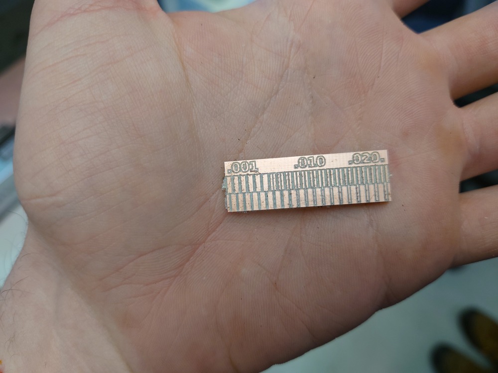
8.2.2.1. Outcomes
0.2mm vbit
track width ~ 0.254mm
clearance ~ 0.178mm
8.3. Individual Assignments
8.3.1. From KiCAD to PNG
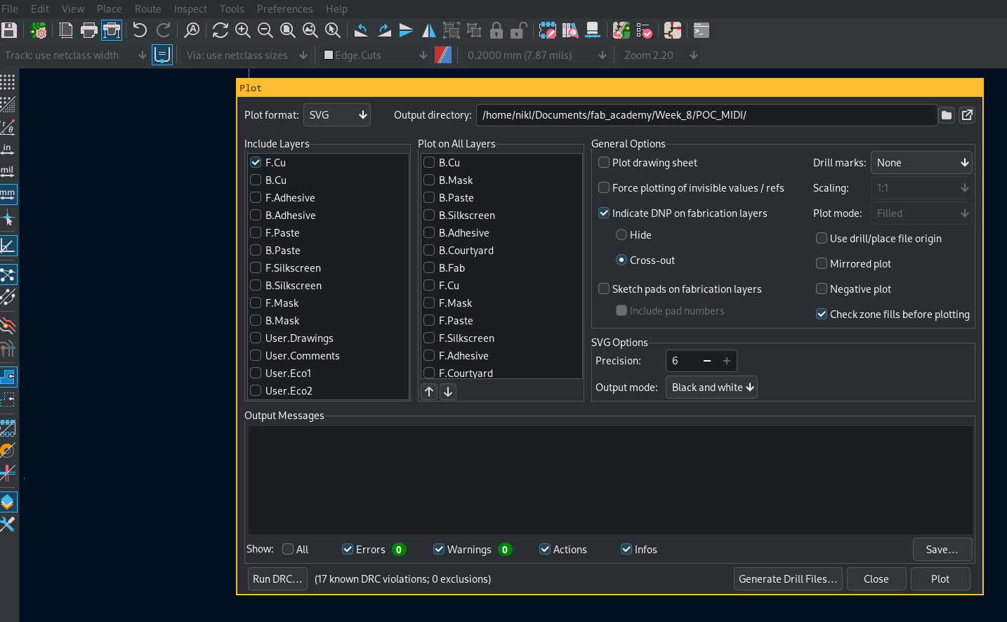
For exporting the paths routed in KiCAD, there are many options (GERBER, SVG, PDF,…) but did it following steps
‘Plot’ (the plot icon next to the printer) the traces and in the popup select ‘SVG’ in the top left dropdown and then select the layers to generate the paths (in my case only ‘Edge.Cuts’ and ‘F.CU’) and then ‘Plot’ in the bottom right.
Open the SVGs in Inkscape, open ‘Document Properties’ and click ‘Resize to content’
IMPORTANT, add a little margin (e.g. 1.5mm, also change from pixel to mm format, if not already) so that lines on the edges are properly recognizes in fab-modules
Select all and center it again (you need to group everything and ‘CTRL+SHIFT+A’, the ‘Align and Distribute’-Tab).
Maybe invert the colors for lines and filled pads (can be annoying, because traces are stroked paths and pads are not stroked but filled shapes -.-), but can also be done in the fab-modules
IMPORTANT for the exterior, the howl board and exterior need to be distinct shapes, NOT PATHs, so it should look like my examples below
Then, if the image and the paths should look right, open the ‘Export’-Tab (CTRL+SHIFT+E), and Export it as a PNG
IMPORTANT set the DPI to ~1000, so the PNG has a high enough resolution for the Fabmodules!!
Then for the milling process, see above
8.3.2. Test Programmer Boards
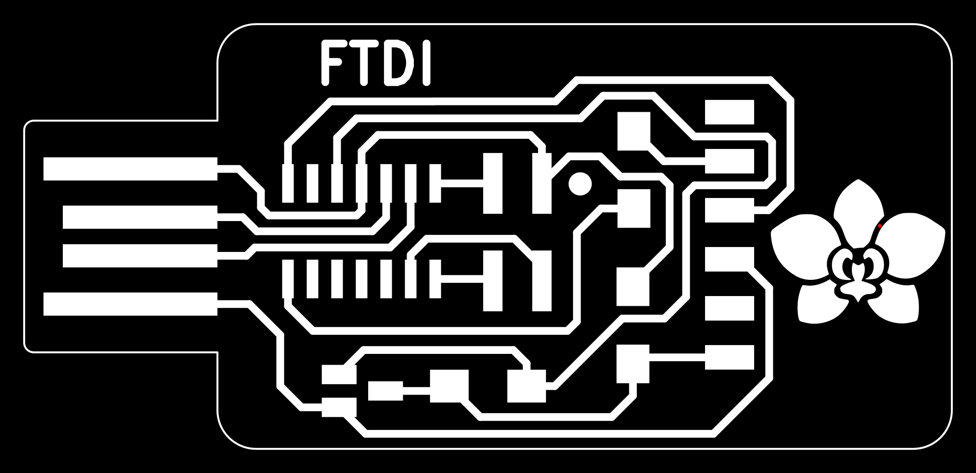
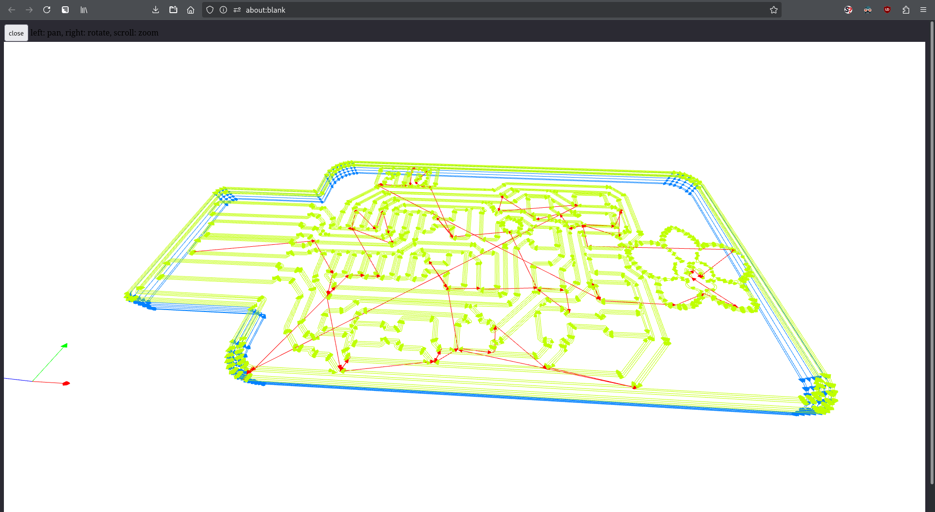
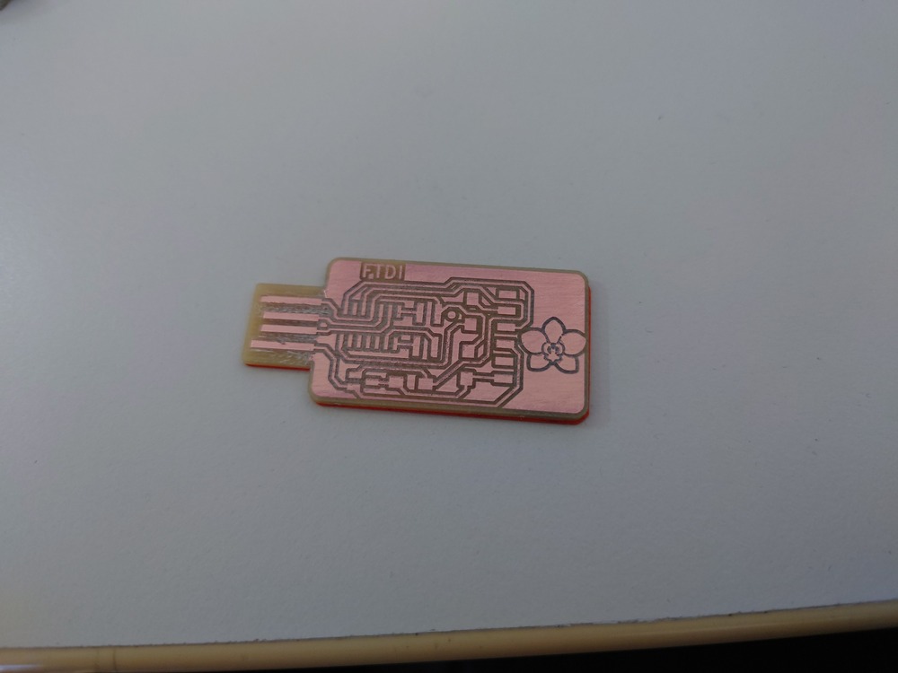
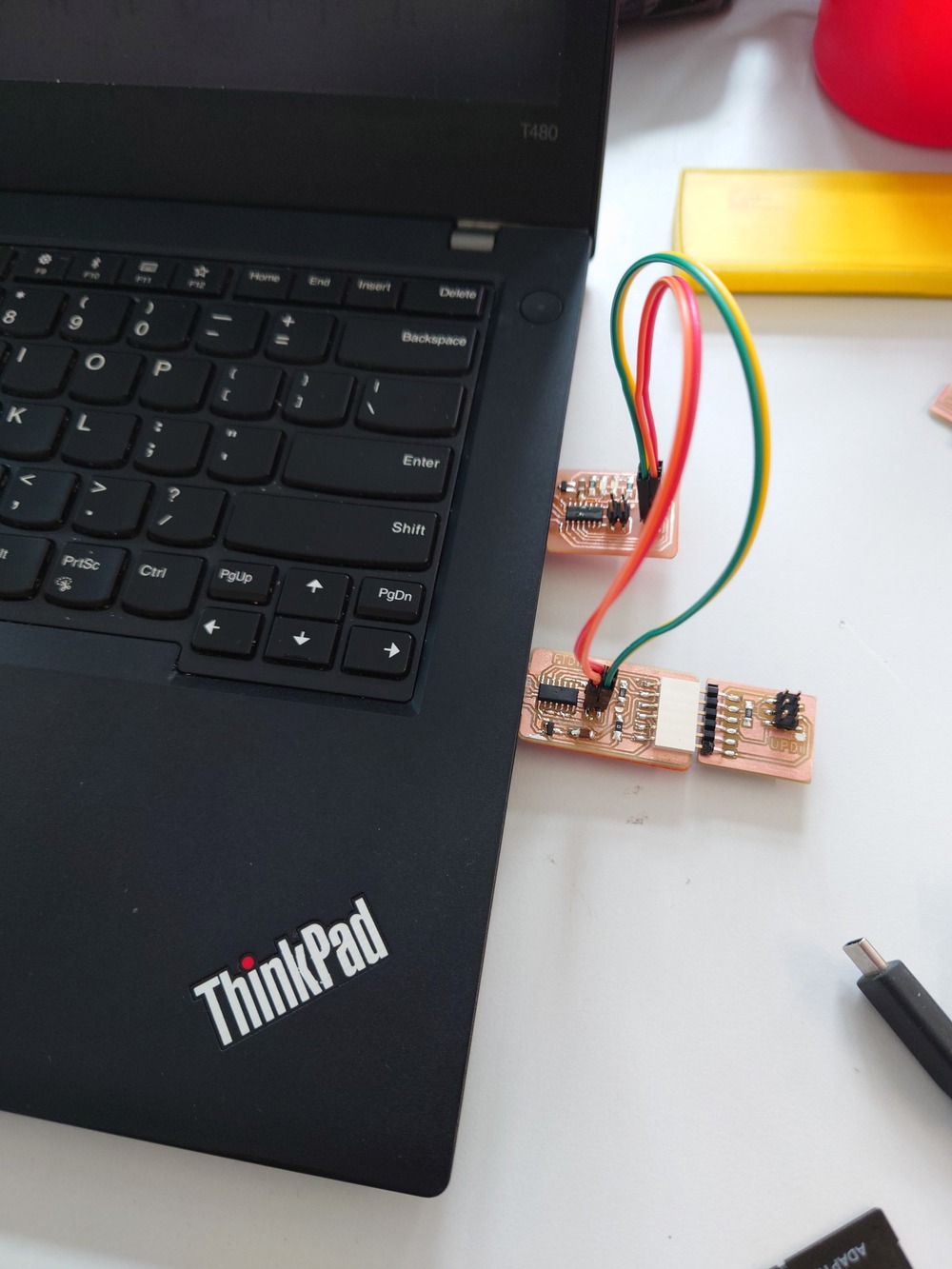
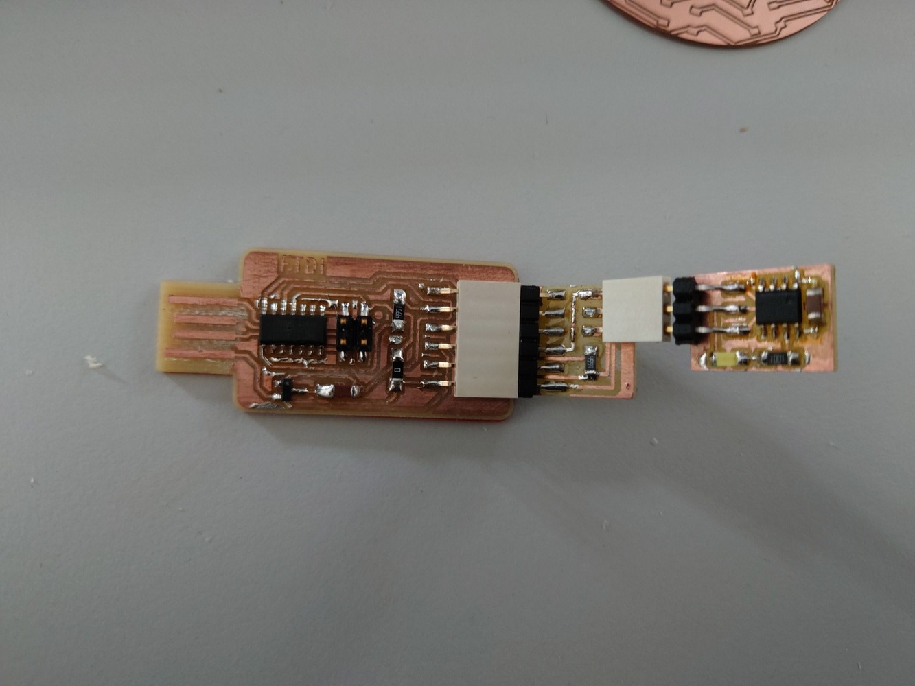
8.3.2.1. FTDI USB Bridge
For testing out above PNG generating method, I first used the USB-to-Serial Bridge from the lecture and adjusted the design-rules in KiCAD (in ‘Board Settings’ under ‘Design-Rules’). Also tried out tracing a bitmap to paths which flowered good.
PNG

GCODE
Milling
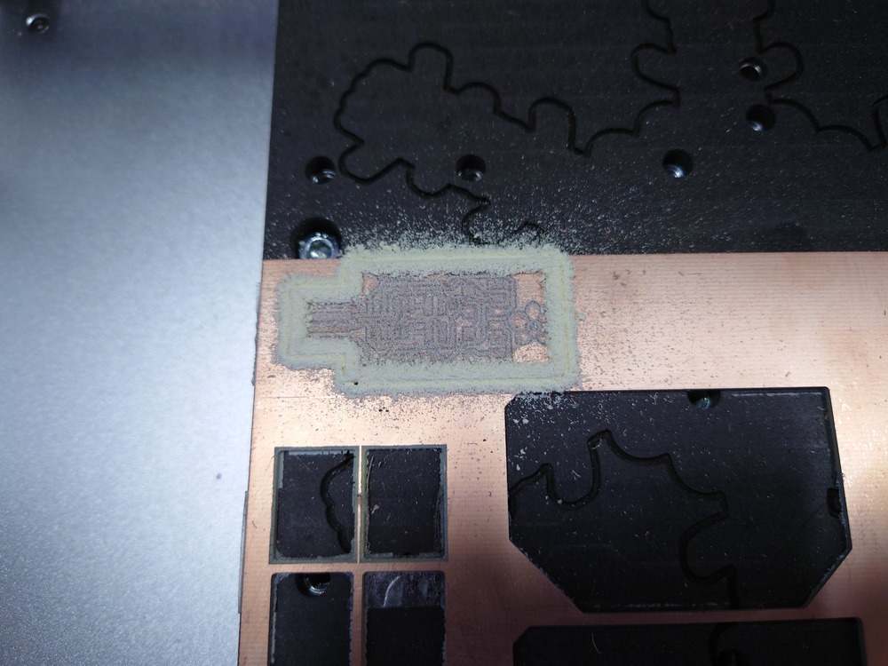
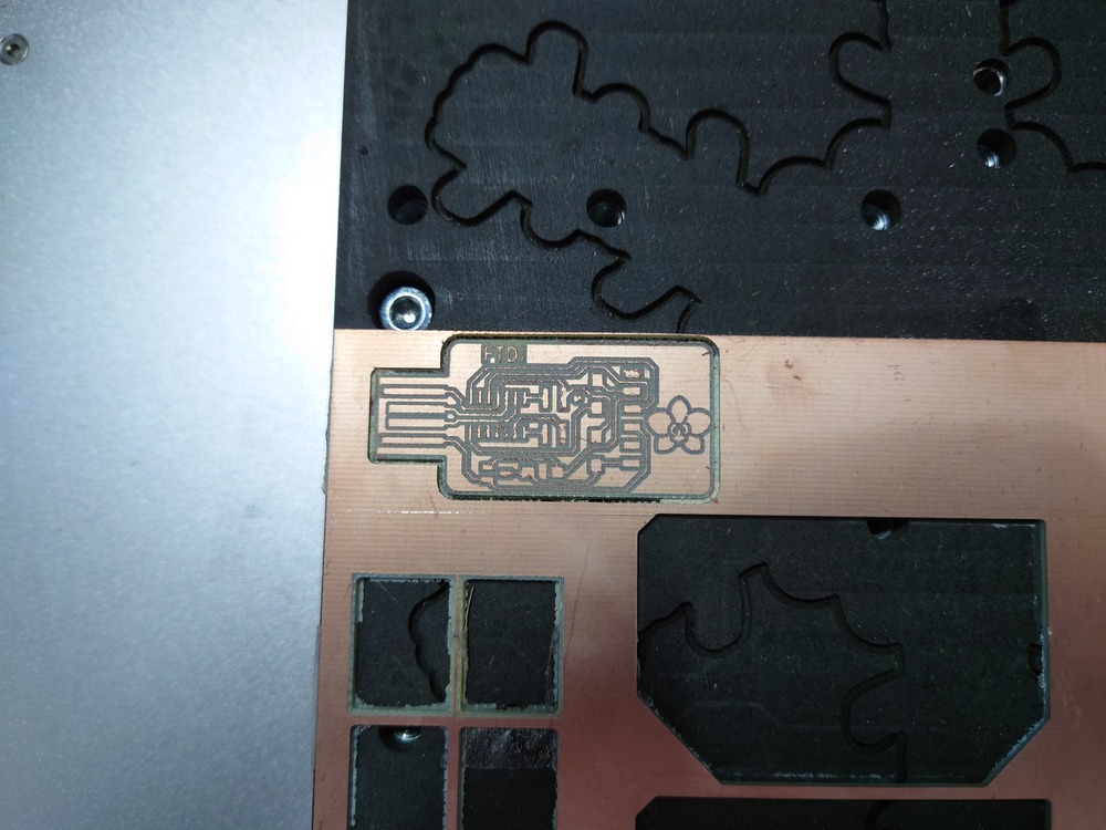
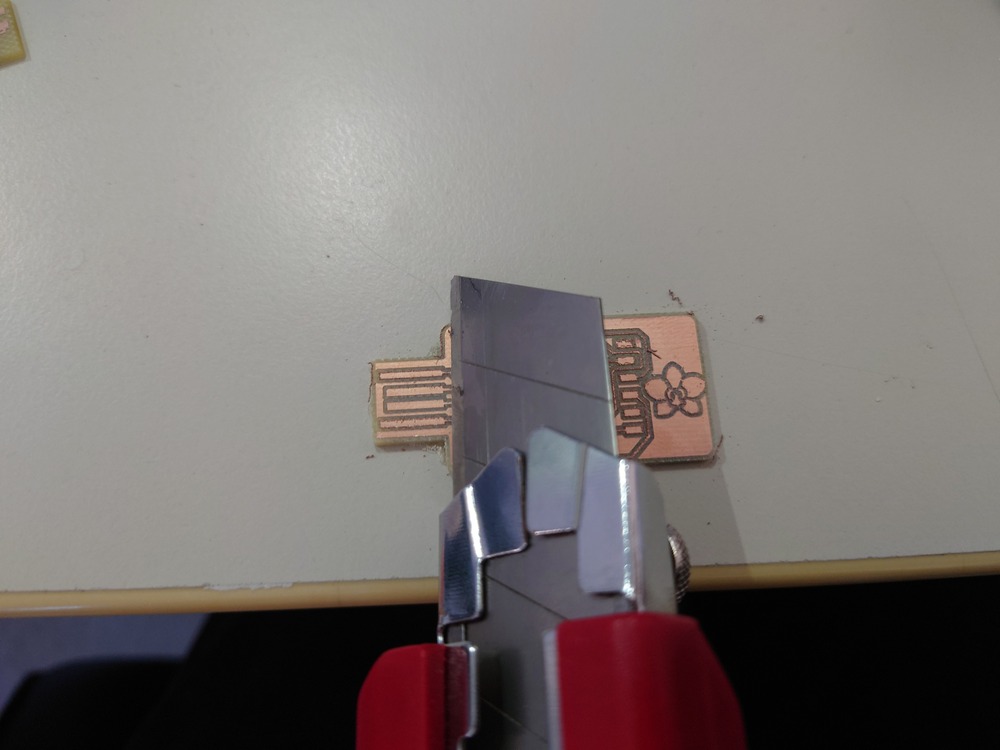
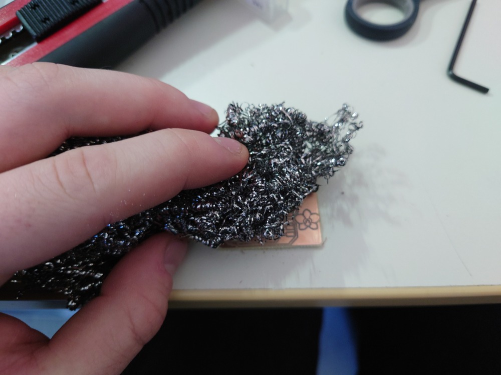
Here I also scratched away the milled traces in the USB connector.
Cutting
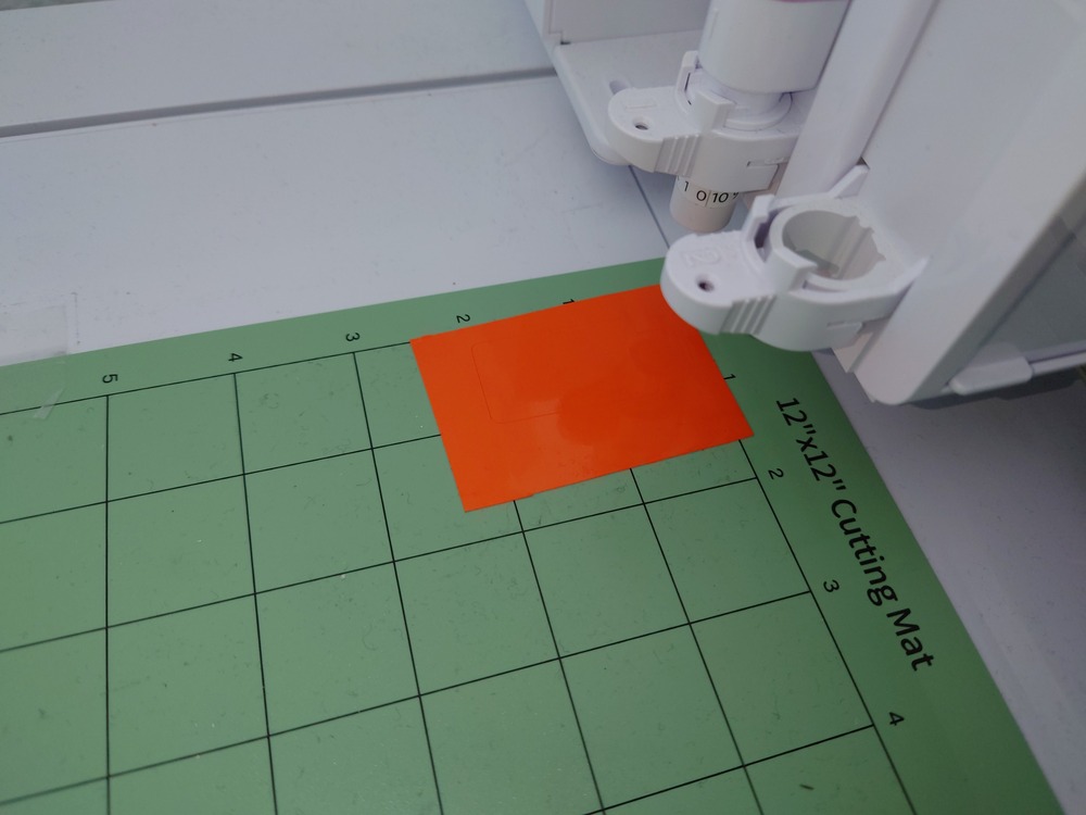
I also cut some vinyl for the back because the PCB is not thick enough for the USB slot.
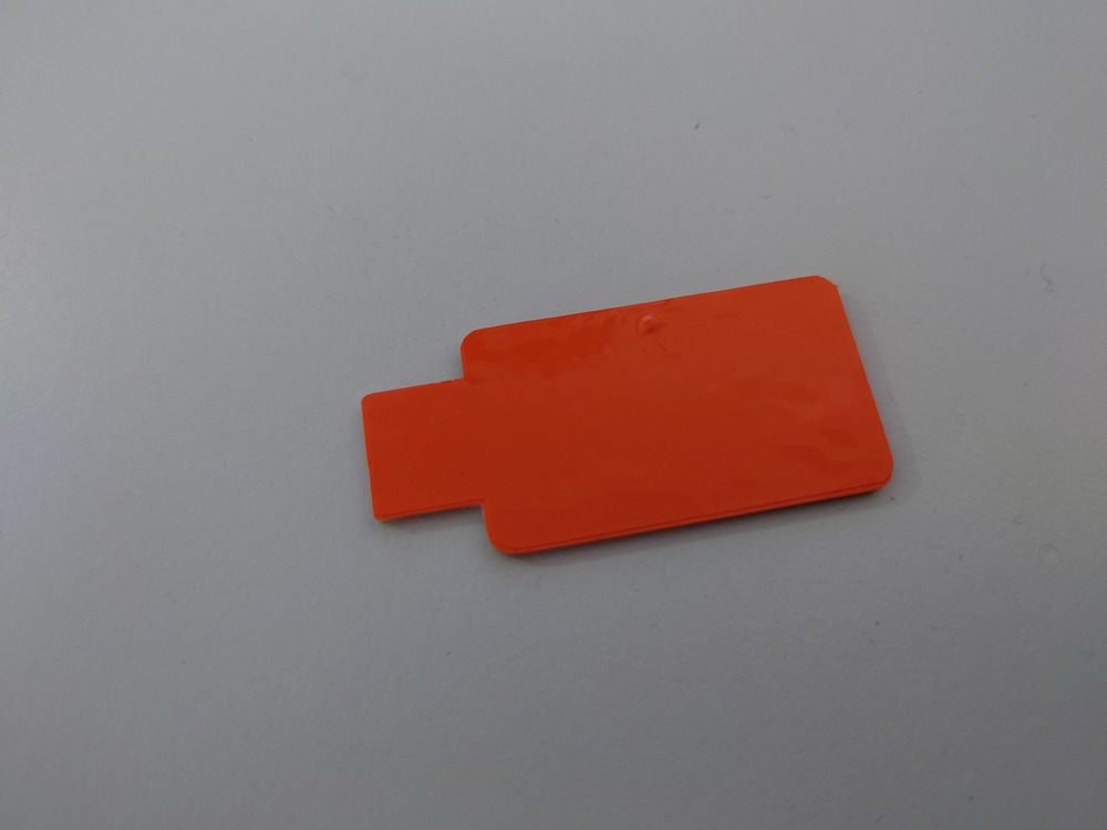
Result
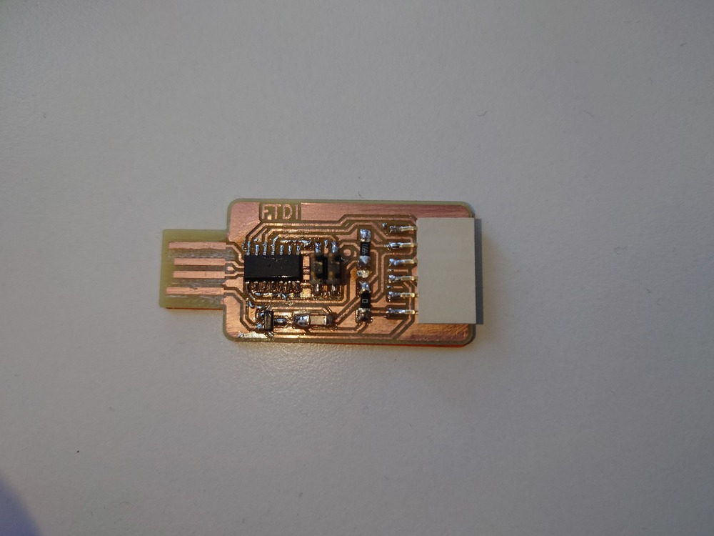
Soldered
On soldering I finally tried out the FLUX technique for soldering an MCU, which works as follows:
first, carefully fix the IC on one pin so that every leg is on the pads
next cover the legs in FLUX (I used a brush)
now use a bug enough soldering iron head and put a bit of solder on it
then slowly and with a reasonable temperature (I used 300°C) scrape with the wide side over the in FLUX covered legs (cover multiple pins at once) until every leg has enough solder
With a bit of practice works very nicely.
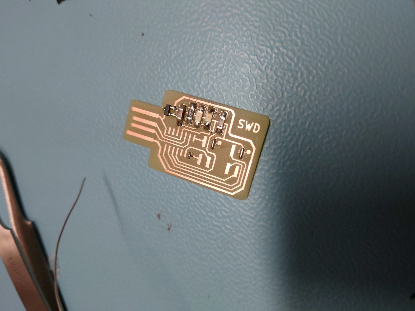
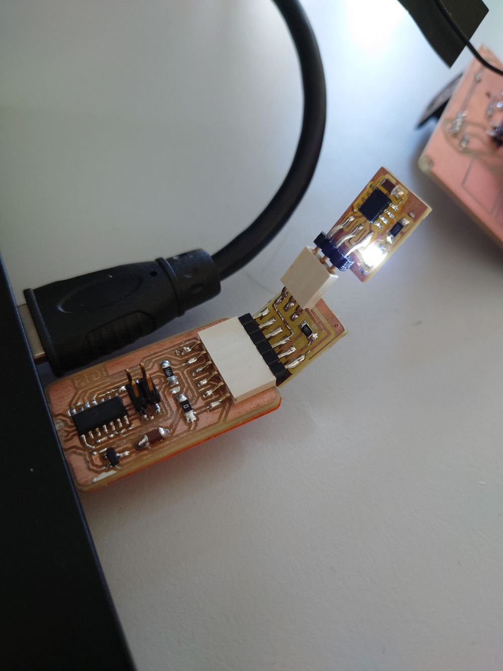
8.3.2.2. SWD Programmer
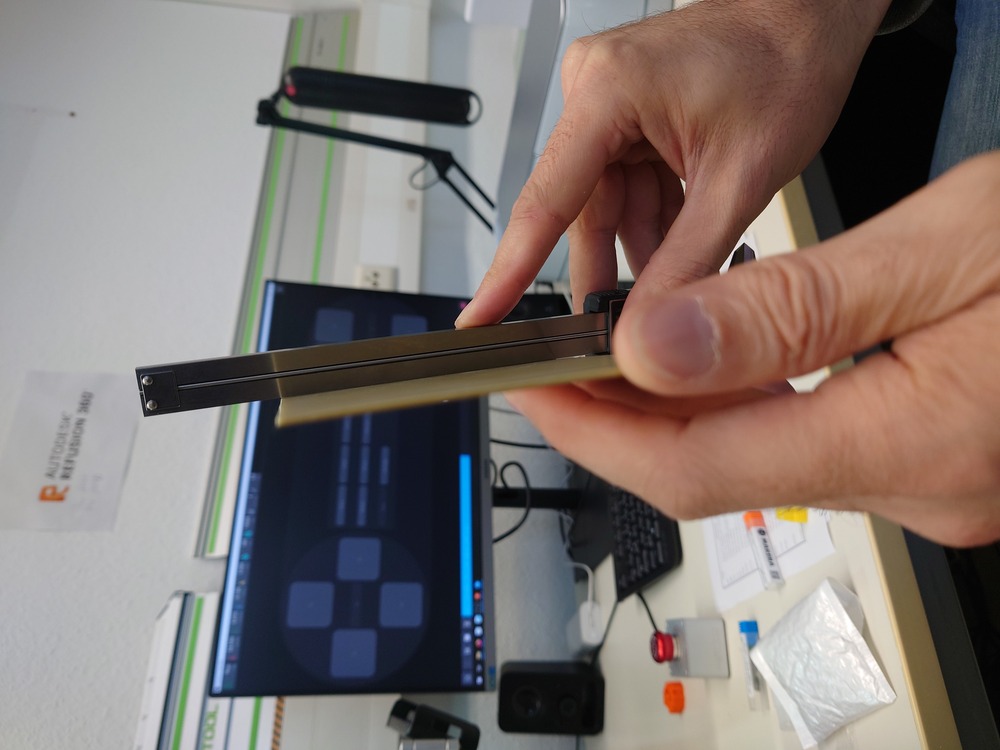
But the above board can’t be programmed, without an SWD programmer, which could also be handy for other boards, so I milled this USB SWD Programmer:
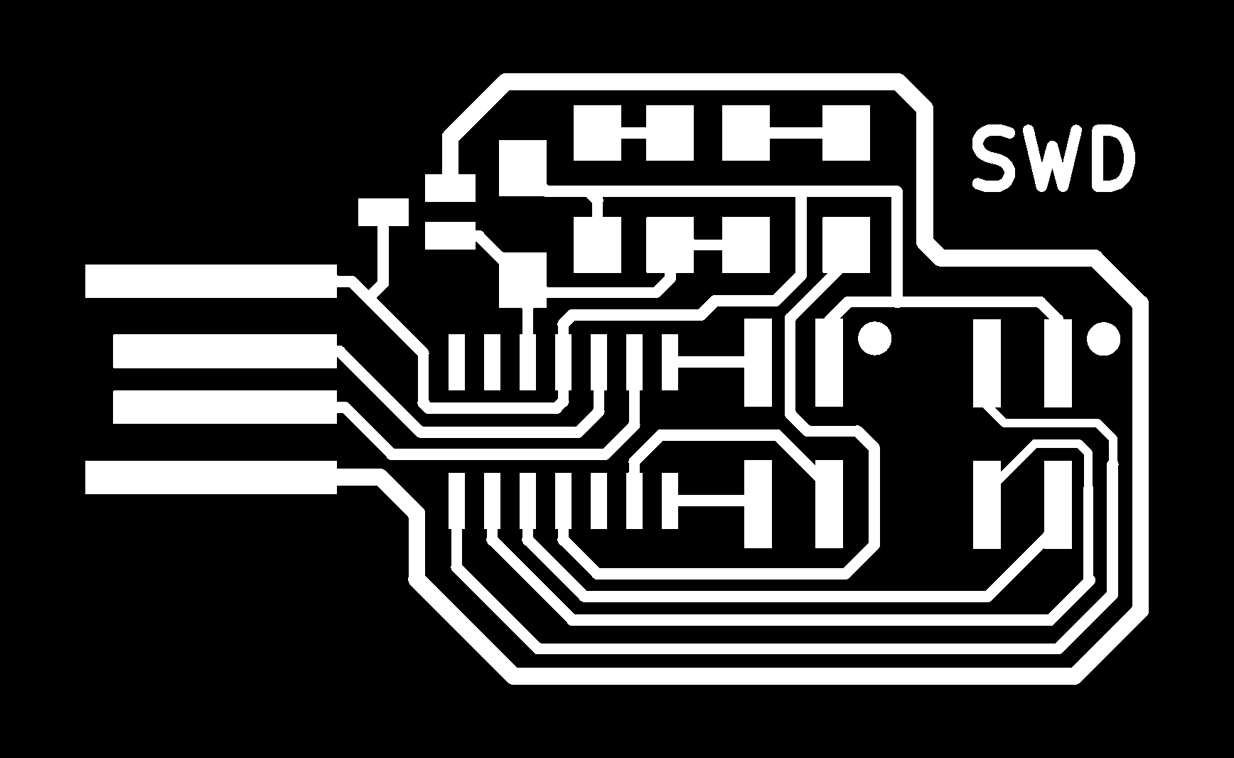

There I also tried out to mill away everything between the parts.
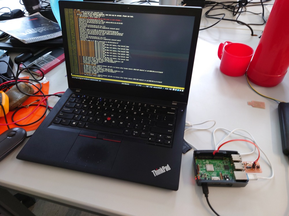
8.3.2.3. Programmer Recursion
Here I thought, I could flash this one directly via USB but I then found out, I also need a Programmer for this one…
NOOOOOOO -.-
But in Neil’s lecture about Embedded Programming, I found a litte article about using the Raspberry Pi for programming via OpenOSC (Github).
So I tried that out as described in the article. For accessing the pi, I used my own network setup, which made some parts a bit more complicated but I didn’t need an extra display, mouse and keyboard :D.
Hint
I used Archlinux for my PI, but I needed following packages:
$ pacman -S base-devel autoconf pkgconf gcc automake
And unfortunately for the configure-step, you need jimtcl, which we need to build from scratch…
And also to work with OpenOSC’s GPIO access, the device /dev/gpiomem needs to be accessible which is not present in the standard archlinux-aarch64 kernel because if the missing kernel-module/build parameter. But fortunately there is the linux-rpi kernel directly from RaspberryPi available:
$ pacman -S linux-rpi
For this to install, you need to uninstall the current kernel and also the uboot-firmware but it will still works!
Note
OpenOSC actually is already build and available via pacman but unfortunately it does not ork with the RaspberryPi config, because the build of the package was not configured with support for gpio pins.. So you need to build it yourself.
I only adjusted following steps of the provided config to work with my device:
# download the formware for the SWD flasher soldered above
wget https://academy.cba.mit.edu/classes/embedded_programming/SWD/free_dap_d11c_mini.bin
Then I followed the instructions from the article and it worked :D.
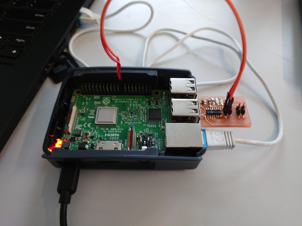
Then I could use the SWD programmer to flash the FTDI programmer with:
edbg -ebpv -t samd11 -f sam_ba_SAMD11C14A.bin
And to test it, I took a small ATTiny board with an LED and…
Blinks!!
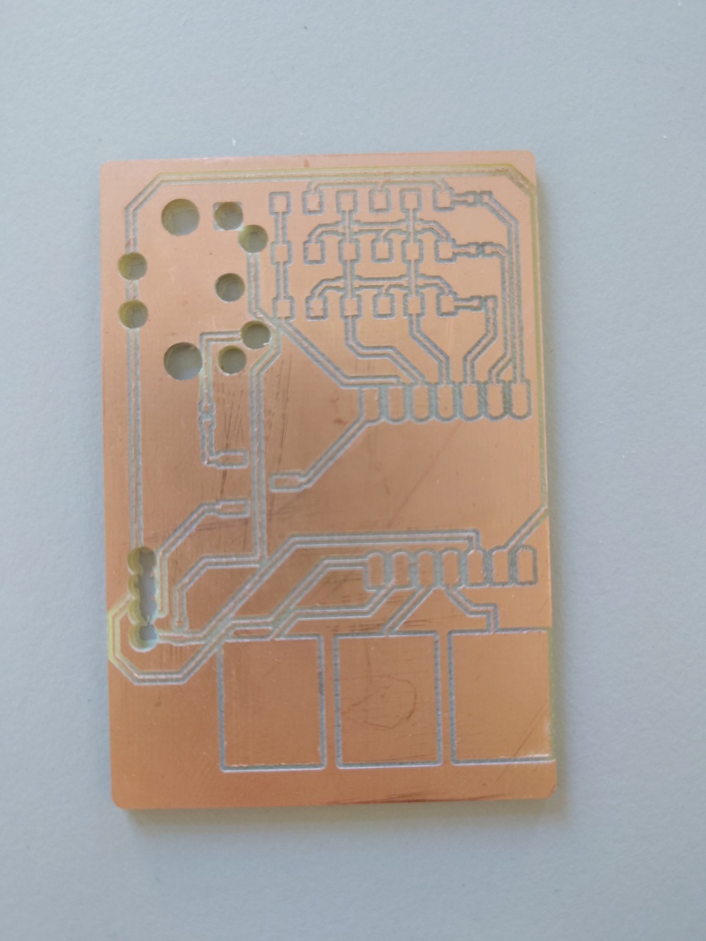
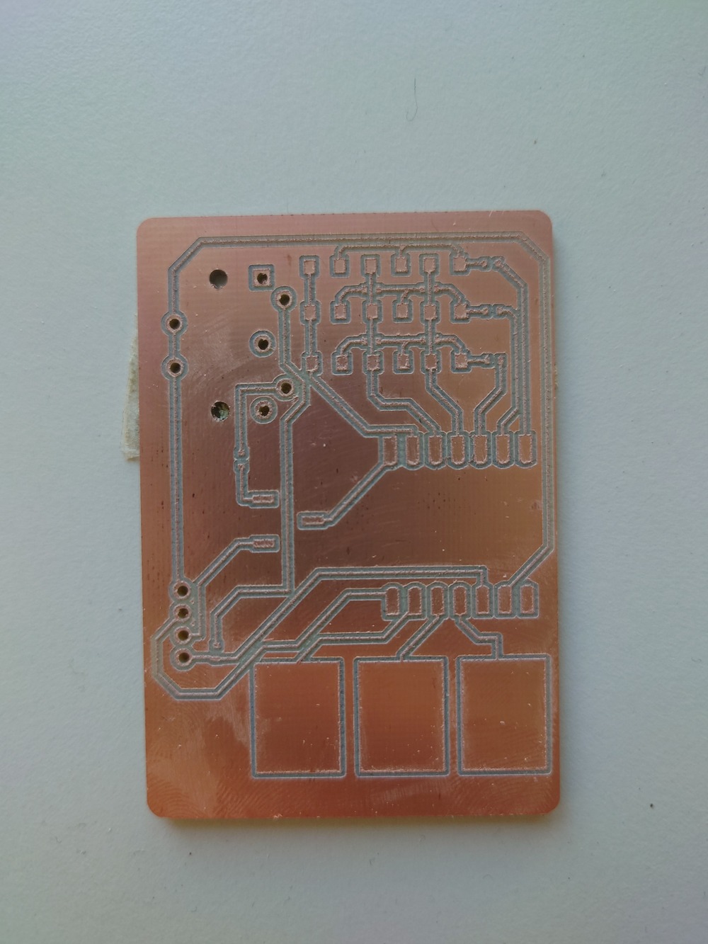
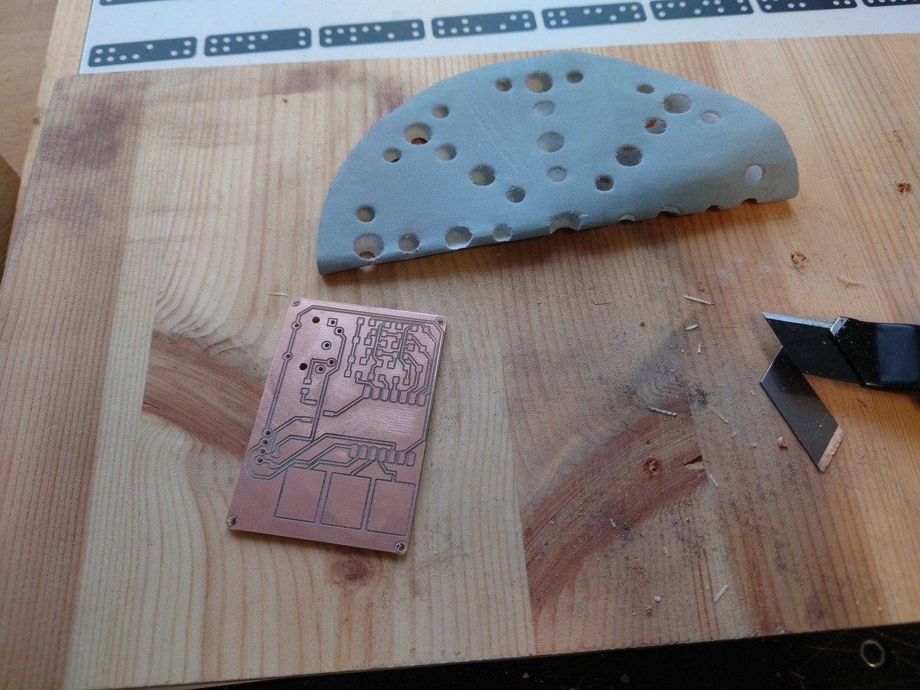
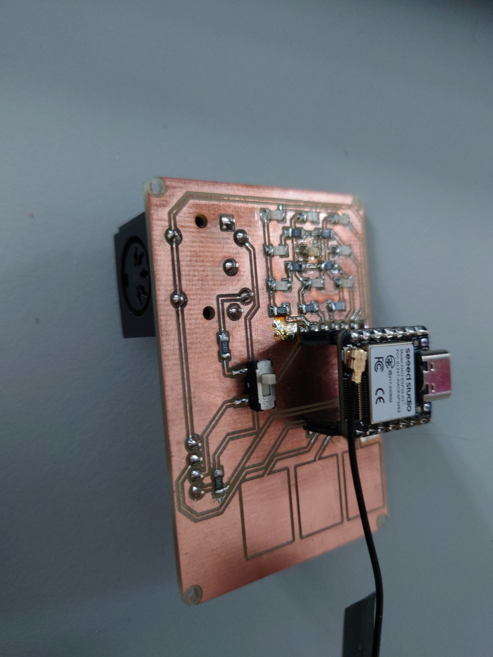
8.3.3. Own PCB
I improved my PCB from the Electronics Design Week, so I fixed the DRC and shortened the board a bit. The tricky part here was milling the hols…
8.3.3.1. PNG
First Images where not inverted, which resulted in way to big holes.
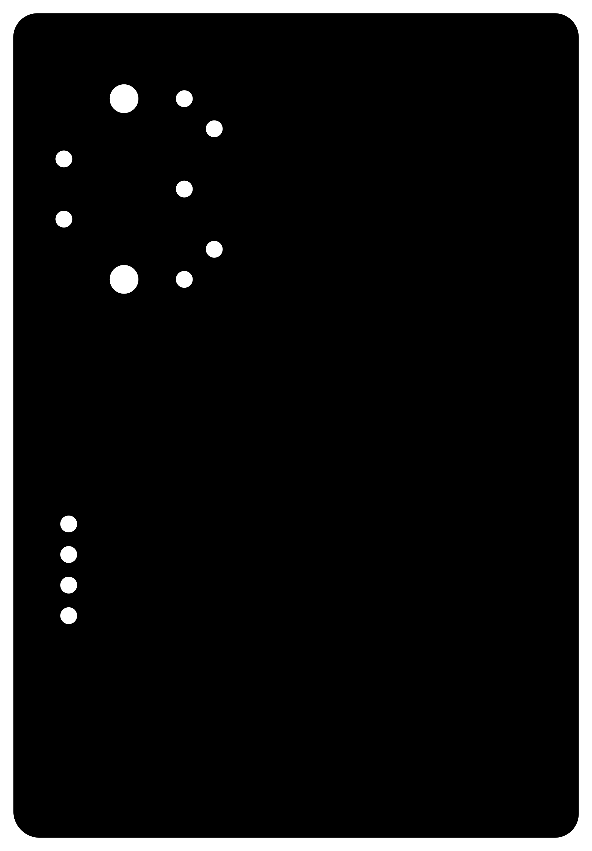
Then I inverted it but there was a weird line in the gcode preview, which was because the inverted version on the right side was not completely black:
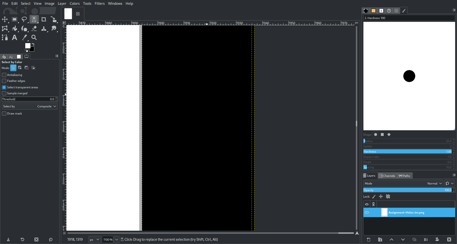
So I fixed it in GIMP and then the path was better.
8.3.3.2. GCODE
Here the weird line from the wrong png.
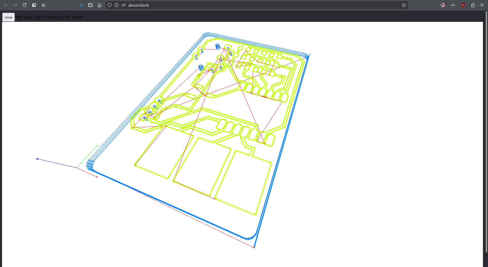
And here with the fixed version:

8.3.3.3. Milling
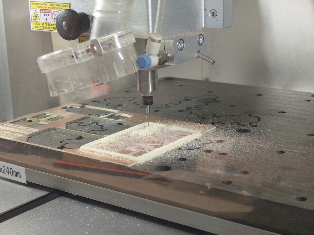
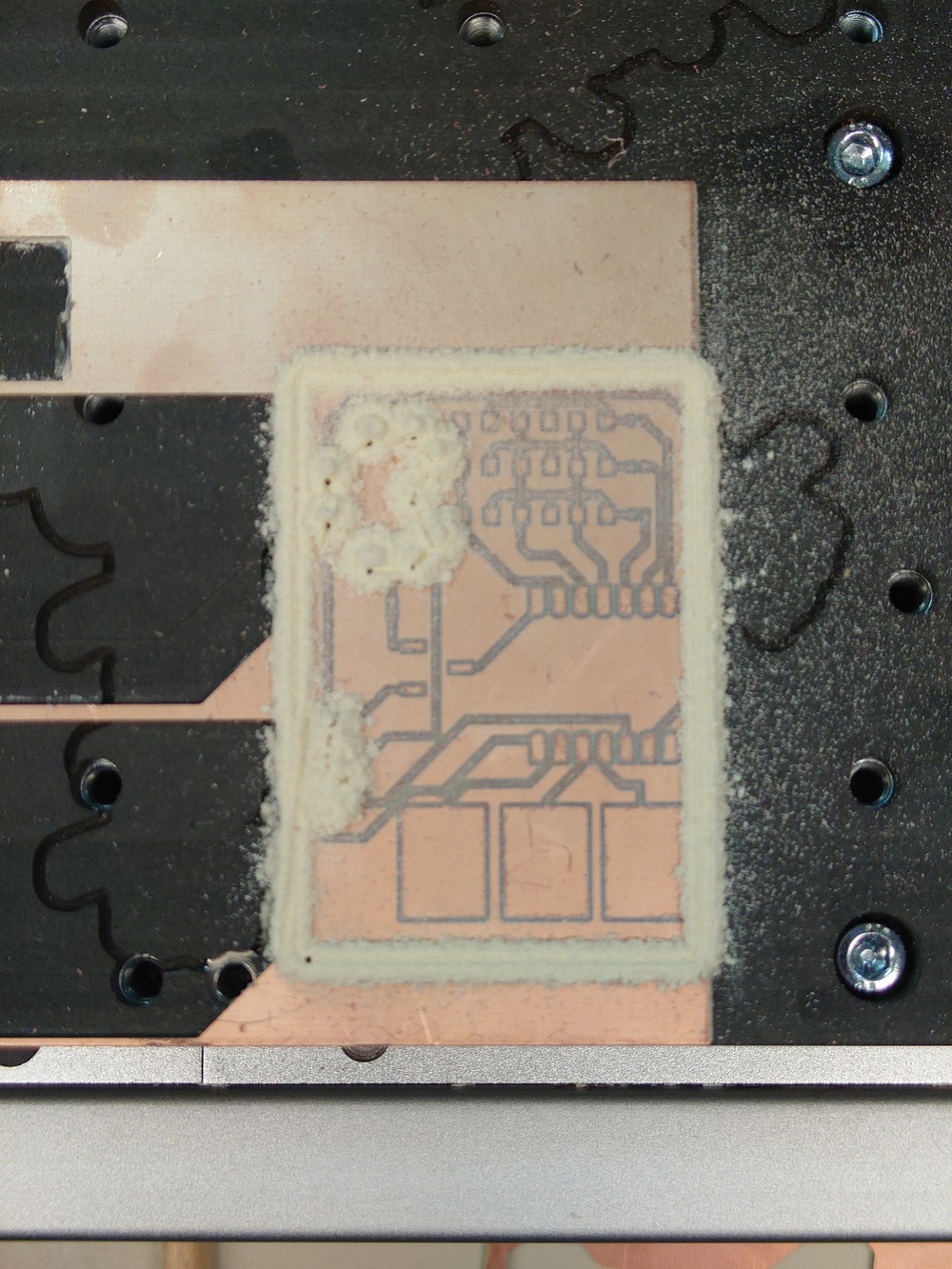
Here the version where I forgot the Inversion:
Here the holes are way to big…
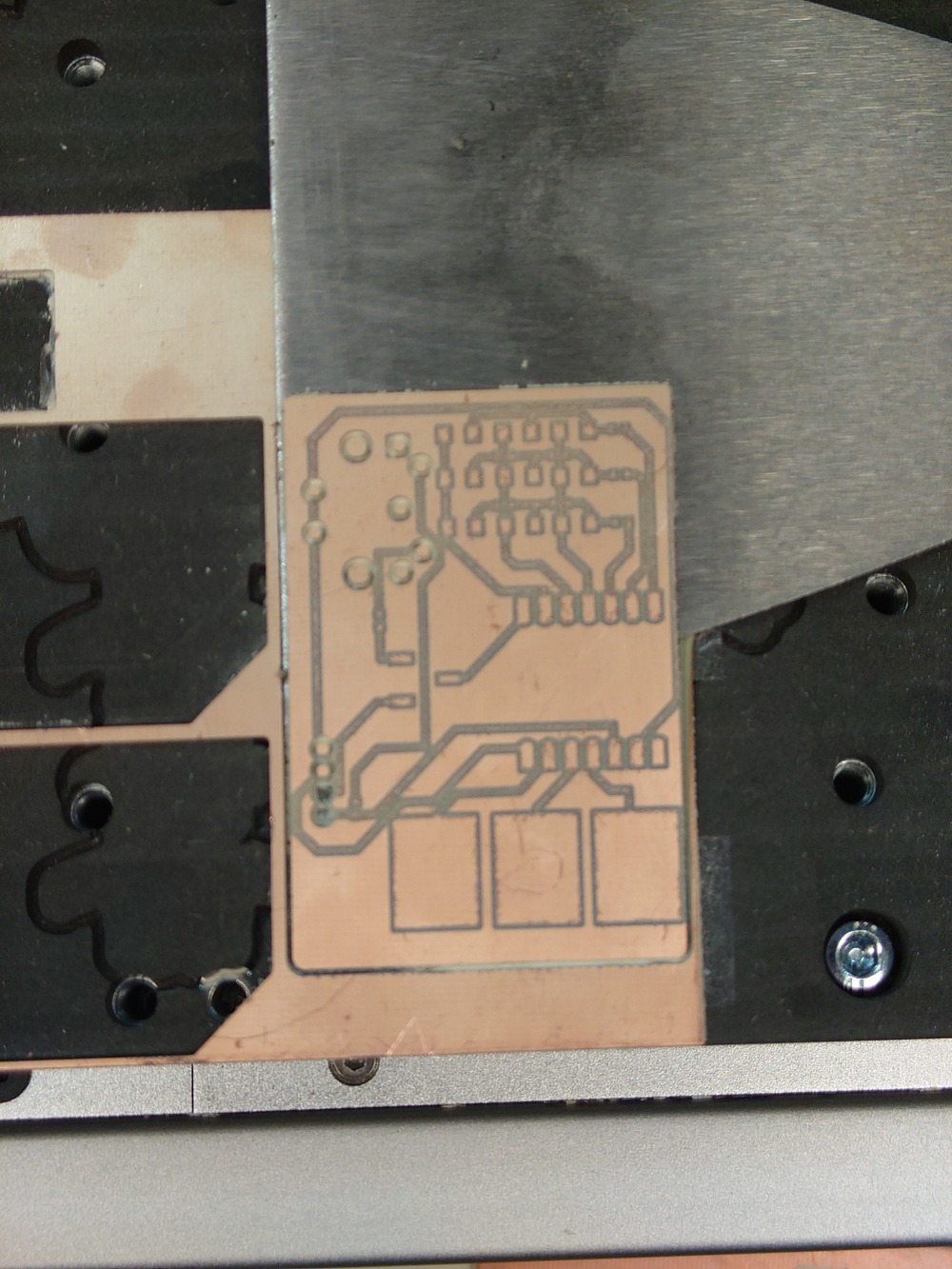
And here the version with inversion:
Better (I know, I didn’t clean it right)
8.3.3.4. Design Fail
After it to me was pointed out, that:
traces are most of the time way to big, I used 0.3mm but 0.4-0.6mm would be better
I used way to small 0-ohm resistors (and also I didn’t needed them at all -.-)
I should place SMD and through hole components on different sides
8.3.3.5. Redesign
So after above things where pointed out to me, I adjusted the design accordingly (changed the midi direction so I can mount it on the bottom, adjusted the resistor footprint and rerouted):
8.3.3.6. Construction
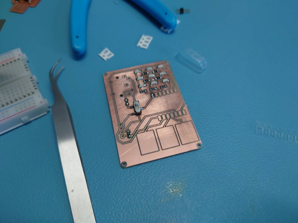
For easier soldering the legs onto the XIAO, I used this little technique ferdi recommended me:
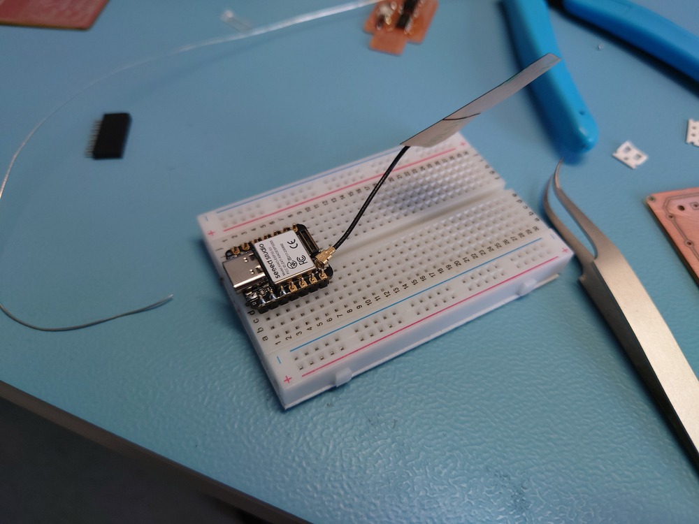 First stick the pins into a breadboard and solder on the MCU.
Then stick the header onto the foots and solder it on for a good alignment.
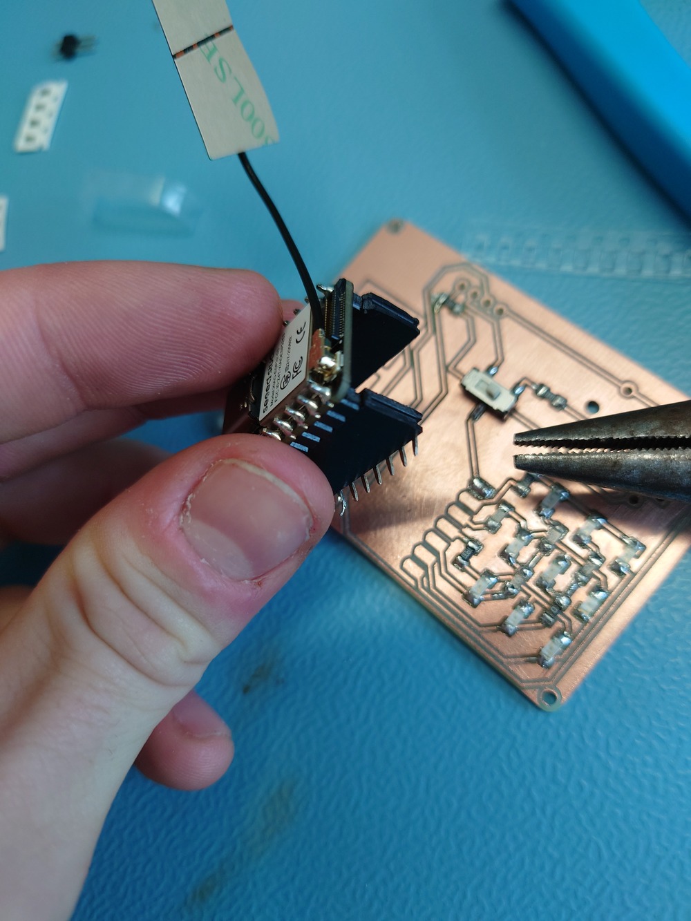
Note
Here I just used tongs to bend the THT header to be an SMD one xD.
I forgot to change the footprint -.-
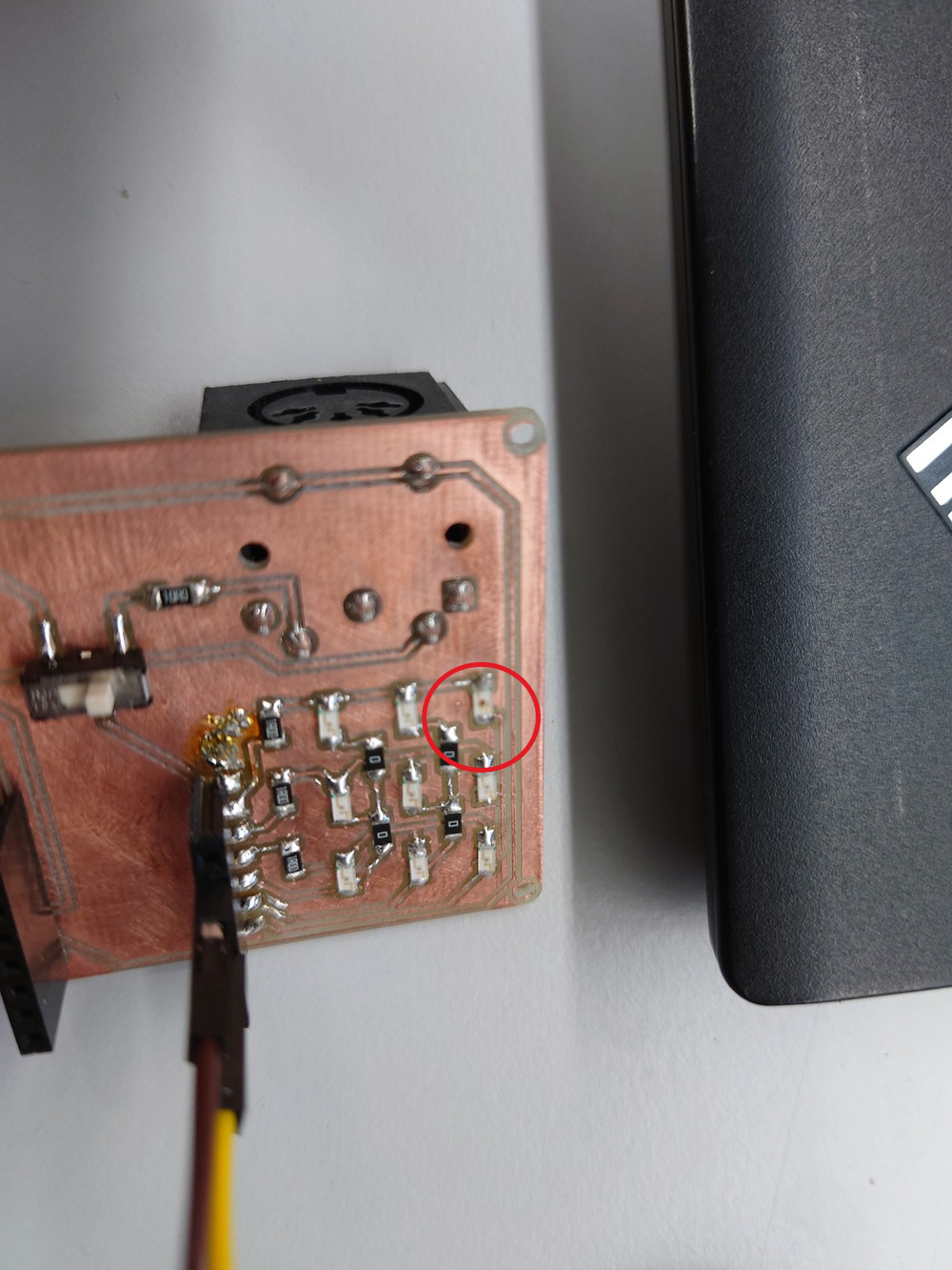
8.3.3.7. Testing
I first test with a laboratory PSU and a multi-meter:
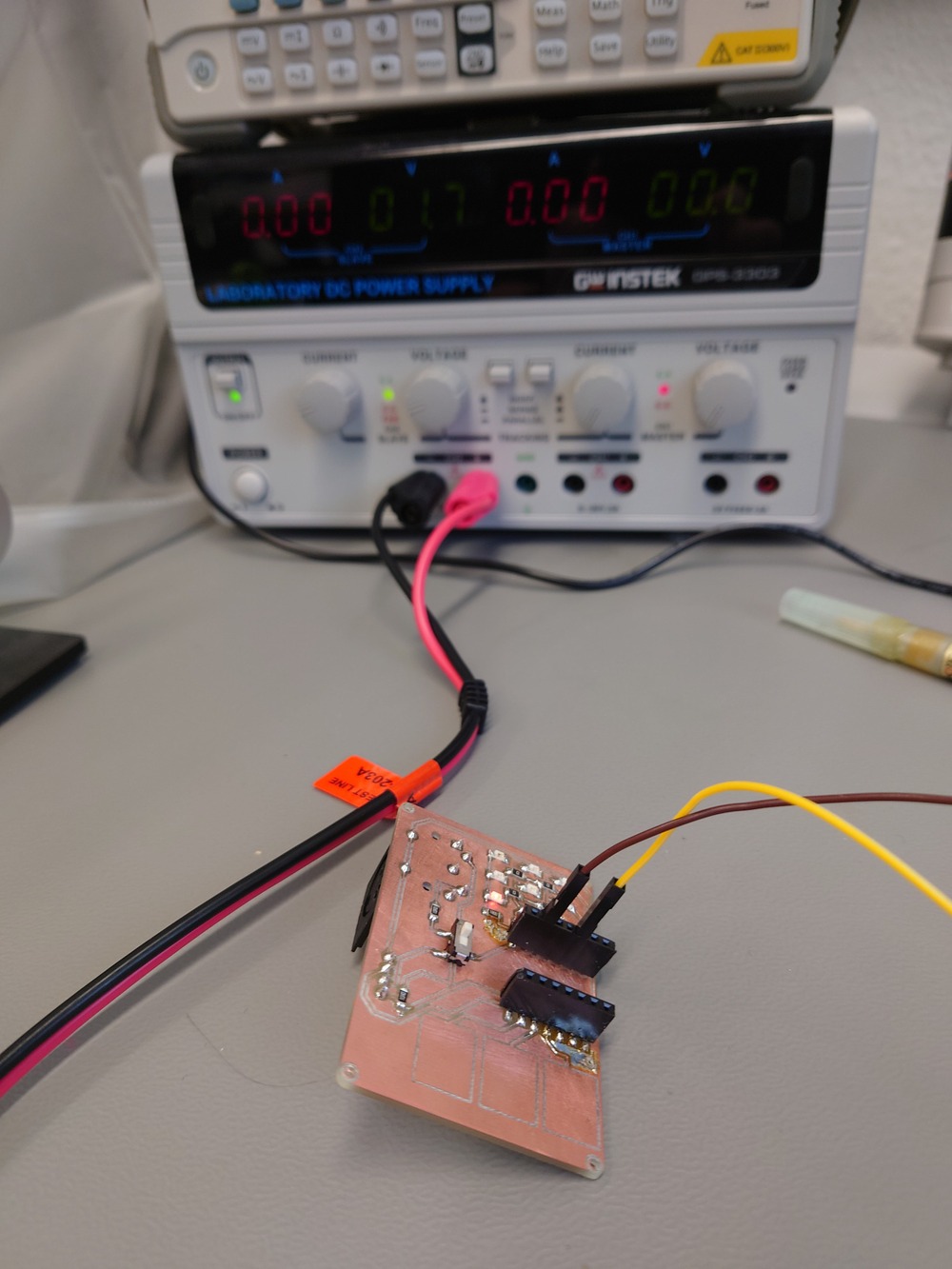
There unfortunately I killed one LED because I set allowed current to high and had the voltage a bit to high -.-
I changed it and everything worked fine without XIAO.
For testing with the XIAO I used just a basic LED Blink example and adjusted it for my matrix:
#include "driver/gpio.h"
#include "esp_log.h"
#include "freertos/task.h"

static const char *TAG = "example";

#define BLINK_GPIO 7
#define CONFIG_BLINK_PERIOD 1000 // in ms

static uint8_t s_led_state = 0;

static void blink_led(void) {
      /* Set the GPIO level according to the state (LOW or HIGH)*/
      for (int i = 1; i < 4; i++) {
               gpio_set_level(i, s_led_state);
  }
}

static void configure_led(void) {
      ESP_LOGI(TAG, "Example configured to blink GPIO LED!");
  for (int i = 1; i < BLINK_GPIO; i++) {
           gpio_reset_pin(i);
    /* Set the GPIO as a push/pull output */
    gpio_set_direction(i, GPIO_MODE_OUTPUT);
    if (i >= 4) {
             // for the matrix, set all negative pins to low
      gpio_set_level(i, 0);
    }
  }
}

void app_main(void) {

      /* Configure the peripheral according to the LED type */
      configure_led();

  while (1) {
    ESP_LOGI(TAG, "Turning the LED %s!", s_led_state == true ? "ON" : "OFF");
    blink_led();
    /* Toggle the LED state */
    s_led_state = !s_led_state;
    vTaskDelay(CONFIG_BLINK_PERIOD / portTICK_PERIOD_MS);
  }
}
And it also worked :D
I then did more about it in Input and Output devices.
8.4. Notes
8.4.1. KiCAD
U .. select entire tracks (may need to be pressed multiple times)
under/near chip small track width
good base track width:
0.4mm
0.6mm
thicker for power lanes
8.4.2. Fab modules
use chrome
offset-number -> rounds around traces
0 == fill/mill all away
think about tool thickness when milling
DRC Check in KiCAD!! (Design-Rule Check)
png dpi >= 500
8.4.3. Carvera
-> make folder for yourself on it (for gcode)
nc .. Numerical Control
PCB-milling z == 0 on top of the PCB
for centering/finding exect x,y zero
‘Edge-Finder’
PCB mill-shank is smaller then wood milling shank
don’t forget ring, if not on it already
check, if tool changer tool is deep in the holes (the plastic ring should be almost in)
adapter for probe if used another shank
always home!!
8.4.4. PCB Milling
RC1 vs RC4 important for design-rules
before milling the PCB, use a hair-ruler to check, it it is straight
most error is the PCB is not fixed enough or it it is not straight enough
PCB glewing very important (double-sided tapes)
thin adhesive, not to strong, no strings/structure strengthener in it
let edges of tape over PCB
look for dirt etc.
don’t need to tape everywhere
press down!
should not move
important -> make sure, baseboard is flat! (just mill it flat)
z-zero-ing needs to be perfect (easily brake mill)