Week 8
Hi! Welcome to yet another week at the Fab Academy, where we move from designing electronics to actually fabricating them. This is an essential step in the journey of digital fabrication, as it allows us to bring our circuit board designs to life.
During this week, we will be expolring different methods of PCB manufacturing, including milling and etching, while we gain hands-on experience with the tools and techniques required to make high quality printed circuit boards.
Types of PCBs
A PCB* Printed Circuit Board is the foundation of most electronic devices, providing mechanical support and electrical connections for various components. PCBs come in different types depending on their construction and flexibility:
-
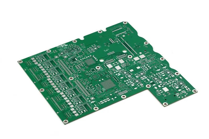
Rigid PCBs: Most common type, made from solid substrates like fiberglass.
-
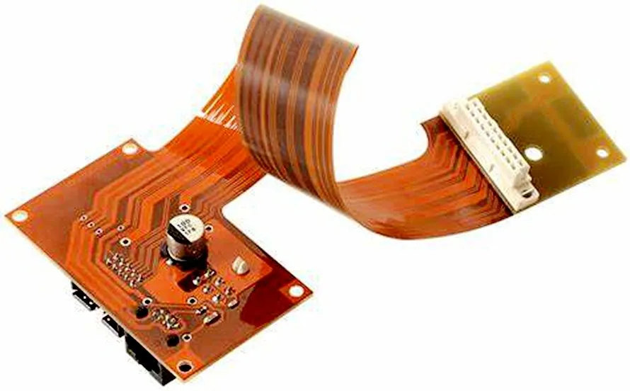
Flexible PCBs: Made from flexible plastic substrates, allowing them to bend and fit into compact spaces, making them ideal for wearable and compact electronics.
-
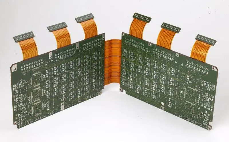
Rigid-Flex PCBs: A combination of both rigid and flexible materials, these PCBs provide structural integrity while maintaining flexibility in certain areas.
In addition to flexibility, PCBs are categorized based on the number of layers and their complexity:
-
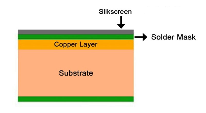
Single-Sided PCBs: The simplest type, with conductive tracks on only one side of the board.
-
Double-Sided PCBs: Have conductive layers on both sides, allowing for more complex circuits and component placement.

- Multilayer PCBs: Consist of multiple layers of conductive material, separated by insulating layers. These are used in high-performance applications like computers and communication devices.
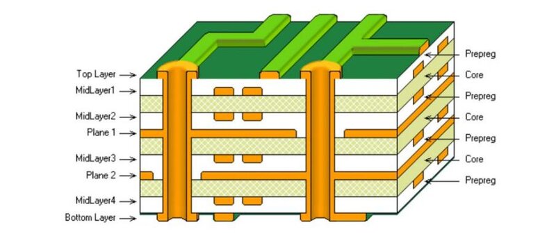
Design Rules & Electrical Connections
When designing a PCB, there are several important design rules to consider to ensure proper functionality and manufacturability:
-
Electrical Conductor Spacing (Clearance): The minimum distance between conductive traces to prevent short circuits.
-
Trace Width: The thickness of conductive paths, which must be sufficient to handle the expected current without overheating.
-
Via and Pad Size: Vias are small holes that connect different layers of a PCB, and pads are the areas where components are soldered. Proper sizing is crucial for good connectivity.
-
Grounding and Power Distribution: A well-planned ground plane and power routing help minimize noise and improve circuit stability.
The are two common fabrication techniques to manufacture a PCB: Etching and Milling.
Etching
This process involves removing unwanted copper from a copper-clad board using a chemical solution, typically ferric chloride or ammonium persulfate. The steps include:
- Printing the Circuit Design onto a special film or transferring it onto the copper board using toner transfer.
- Etching the Board by immersing it in an etching solution to remove the unprotected copper.
- Drilling Holes for through-hole components, if necessary.
- Cleaning and Finishing the PCB to remove any remaining chemical residues.
Etching is great for high precision traces but involves handling chemicals and requires proper disposal of hazardous waste ☢ . So lets check out another met
CNC Milling
Milling uses a computer-controlled milling machine to carvehod... out the PCB traces and pads from a copper-clad board. The process involves:
- Generating G-code from the PCB design file.
- Using a CNC Machine with an endmill or engraving bit to remove unwanted copper.
- Drilling Holes and Cutting the Board to its final shape.
Milling is cleaner and faster than etching and does not require chemicals, but it has limitations in terms of minimum trace width and resolution. We'll see more about this further on, stay with me!
Alternative Fabrication Techniques
-
Fiber Laser Engraving: Uses a high-powered laser to selectively remove copper, creating traces without using a milling bit. This method offers high precision and is ideal for fine-pitch components.
-
Vinyl Cutting for PCB Masking: A vinyl cutter can be used to create stencils for etch-resistant masks, which help define the circuit pattern before chemical etching. You can stick this circtuits on tridimensional surfaces!
Soldering
Soldering is the process of attaching electronic components to a PCB, ensuring reliable electrical connections. Check out our Group Documentation, where we include some tips our local instructor taught us ;)
So, essential tools:
- Soldering Iron: Heats and melts solder to join components.
- Solder Paste & Flux: Improve adhesion and conductivity.
- Tweezers & Magnifying Glass: Aid in precise component placement.
Reminders:
- Keep the soldering iron tip clean.
- Apply heat to both the pad and the component lead.
- Use the right amount of solder to avoid shorts or weak connections.
You can see how it's done in this video, old as time but still, surprisingly effective.
OK! Its time to make some dreams come true.
At our local lab we have a Roland MonoFab SRM-20 milling machine that comes with its own software in order to take instructions.
Esentially, the workflow of this process looks like this:

Preparing the File
I'll be using the board I created on Week 6 and an outline from a vector leaf I created.
Go to Kicad, and in the PCB editor and click on Print > Print > PDF and name the file and the folder you want to save it in.

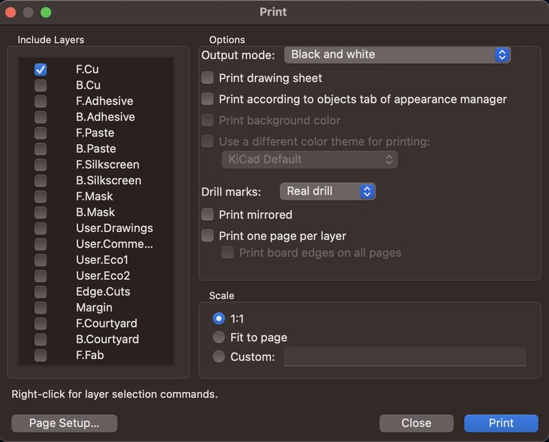
Here you can select what information you want to export. In our case we will be exporting only the Front Copper because I will be creating the outline on Illustrator.
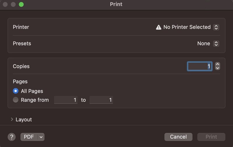
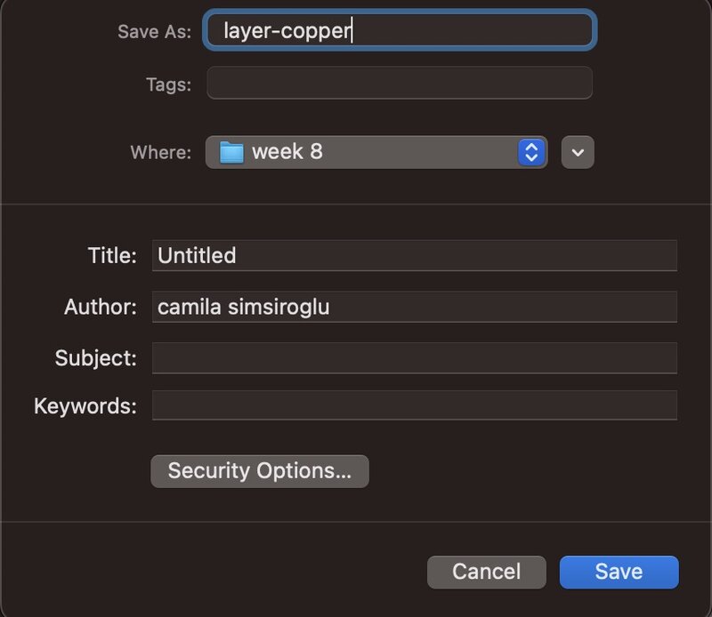
This will create a PDF file with the information you need to mill. Ideally, this is what we are aiming for:
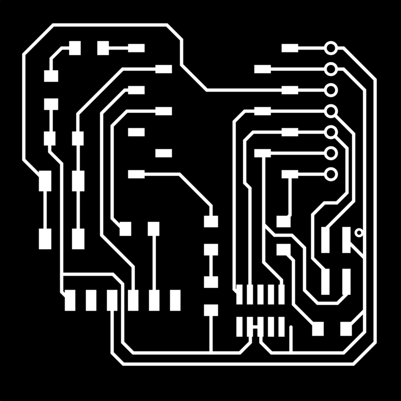


Open this in your favourite vector software, as I said, I'll be using Adobe Illustrator. Ok, the process was a little tricky on this software but here is how I made it work.
I started out with this vectorized image and added a colored background to makes things clearer.
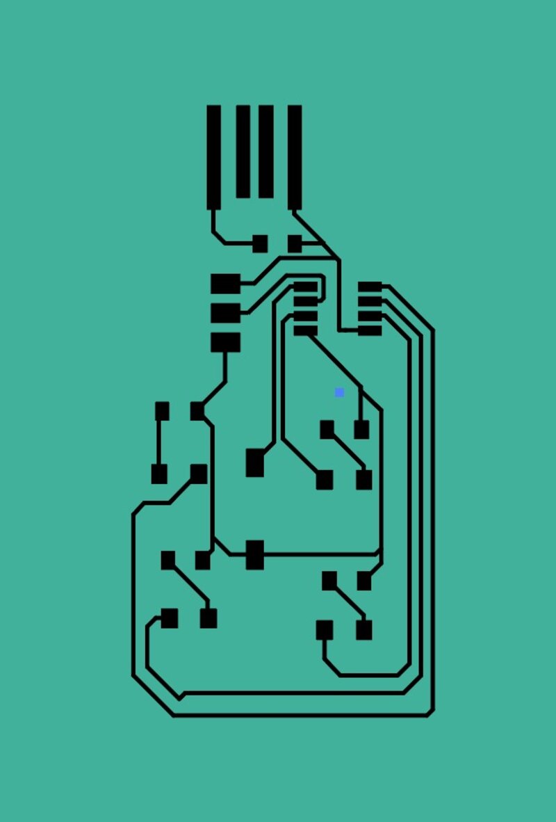
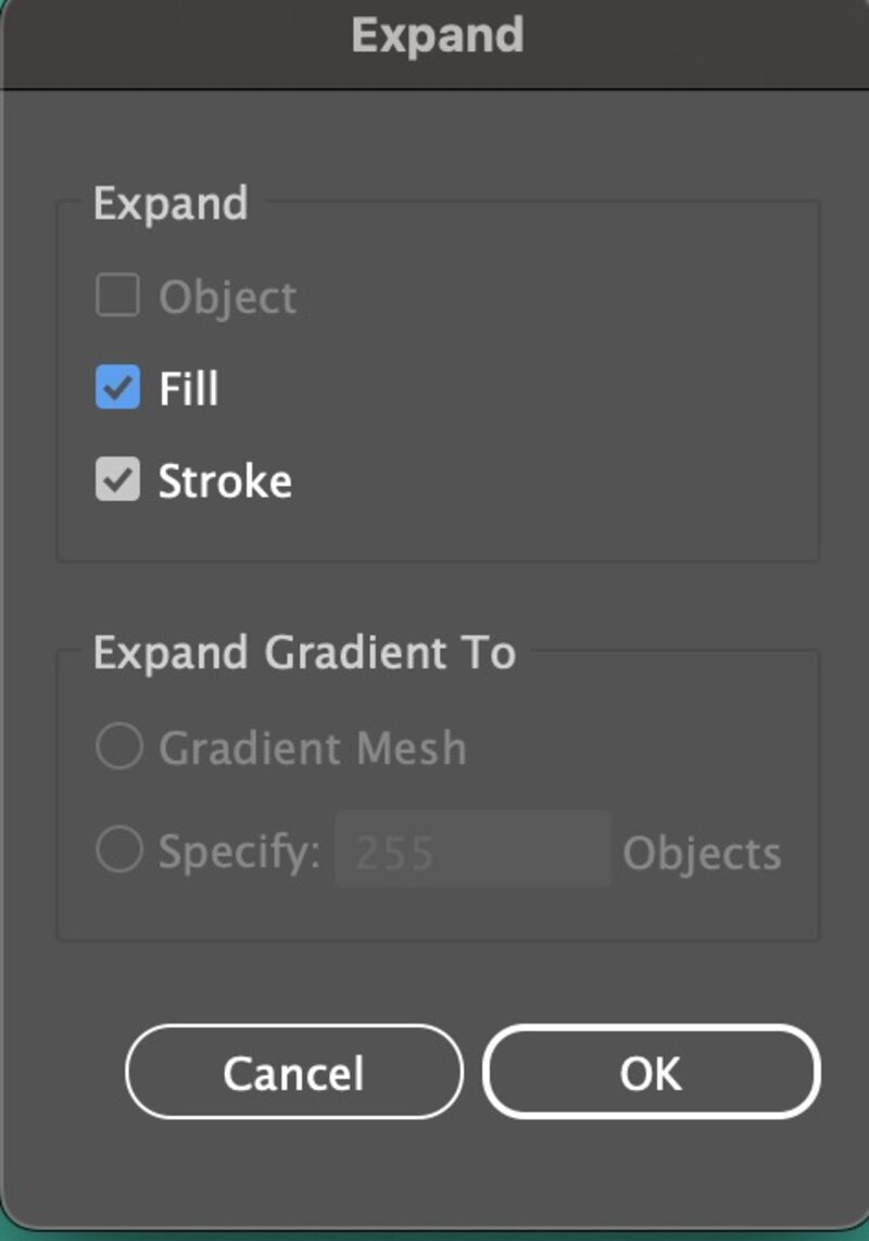
Then, I chose Object > Expand everything over everything.

Now go over to the Window tab and open the Pathfinder.
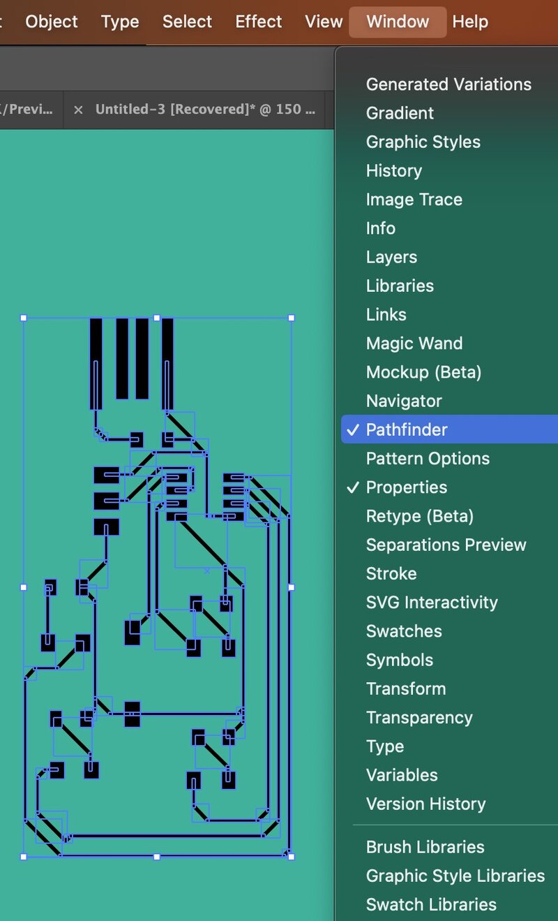
First, click on the second option of the Pathfinder. Then click on the Unite option of the Shape Mode.
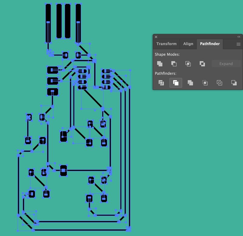
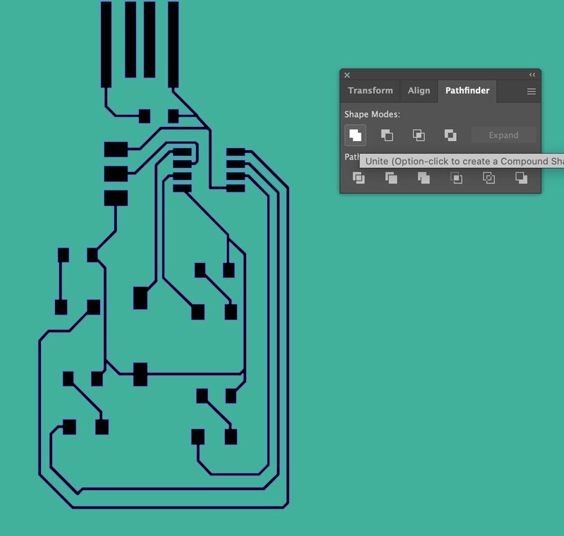
And Voilà :D You can now change the color of your outlines to get an inverted PNG that looks like this!
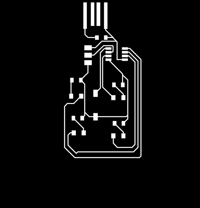
Here is the outline:

Cool! So... what's next? Oh yes! The mods! But wait. What is a "Mods"?
Mods is a browser-based, open-source tool that converts PCB designs into milling toolpaths. Much like a slicer for CNC machines or 3D printers. It customizes workflows, supports various machines (like the Roland SRM-20), and requires no installation.
Go to the website, right click > program > open program > select your machine (Roland, milling PCB).
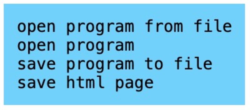
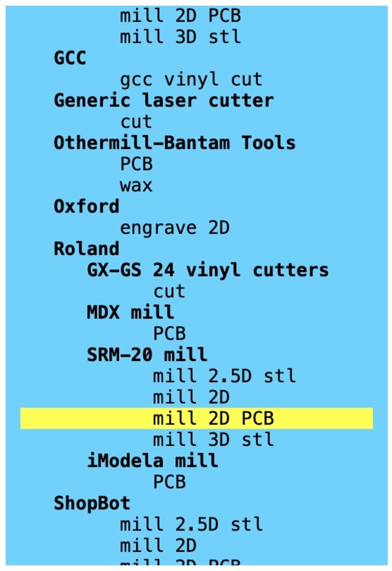
You should be looking at something like this:
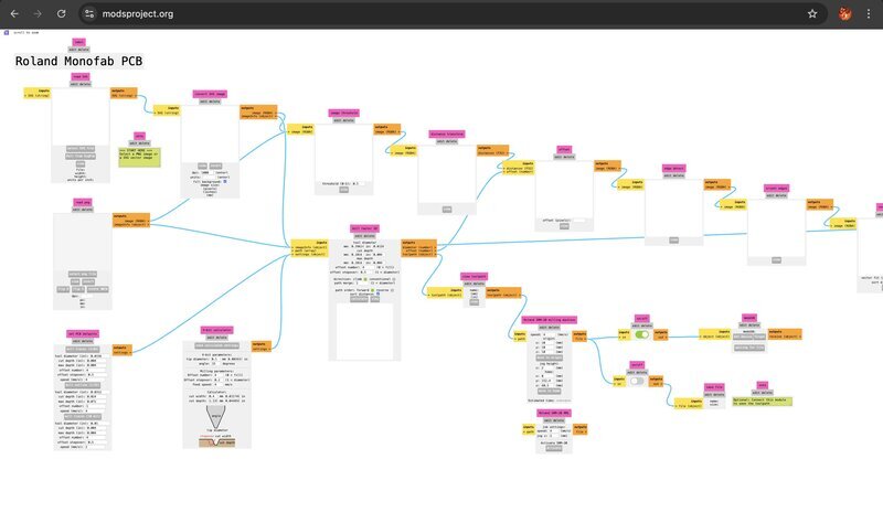
Now load your .png, I'll be starting with the traces. Remember to export it with 1000.dpi resolution. Go to set PCB defaults and click on Mill Traces, which is what we are going to to first (Mill Outline otherwise).
You should be looking at something like this:
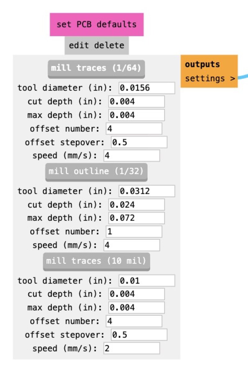
Now you should see some default settings here at mill raster:
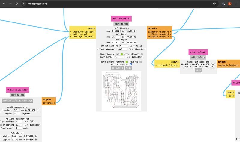
When you are tracing, set your cut depth and max depths to 0.15 mm (holy precision). When outlining, leave these settings on default.
Enable your edit delete outputs and set your milling machine speed to 2 and your X,Y and Z values to 0 (This goes aswell in the outline and drill options).
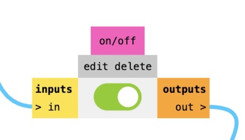
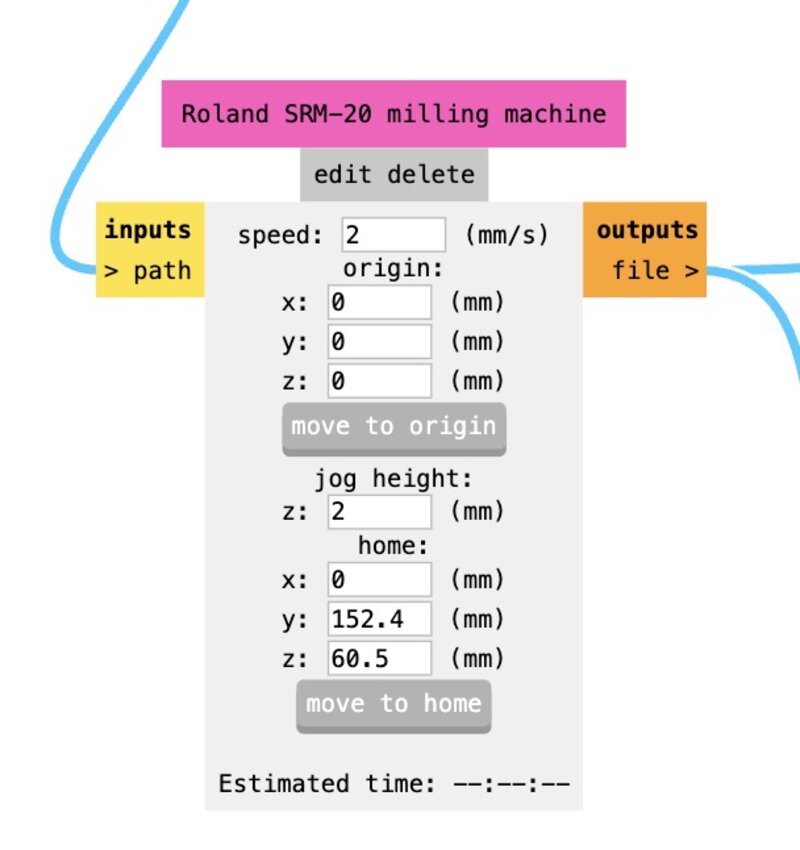
Now click on calculate and this will create a cut file for your SRM-20 MonoLab software.
Cutting
Head over to the Roland machine and use the Vpanel for SRM-20. First up, place your mill in the machine. At our lab we have 1/64 (tracing) and 1/32(outline and holes) in size.
Pick your weapon (tracing first) and insert it in the clamping collect. Inside the Roland you'll find an Allen tool to adjust your mill. Leave a 3-5mm distance above the plate.
Place your copper board on the cutting base and fix it by using some double-side tape on the bottom of your board. Make sure there are no wrinkles.
This is how the software looks like.
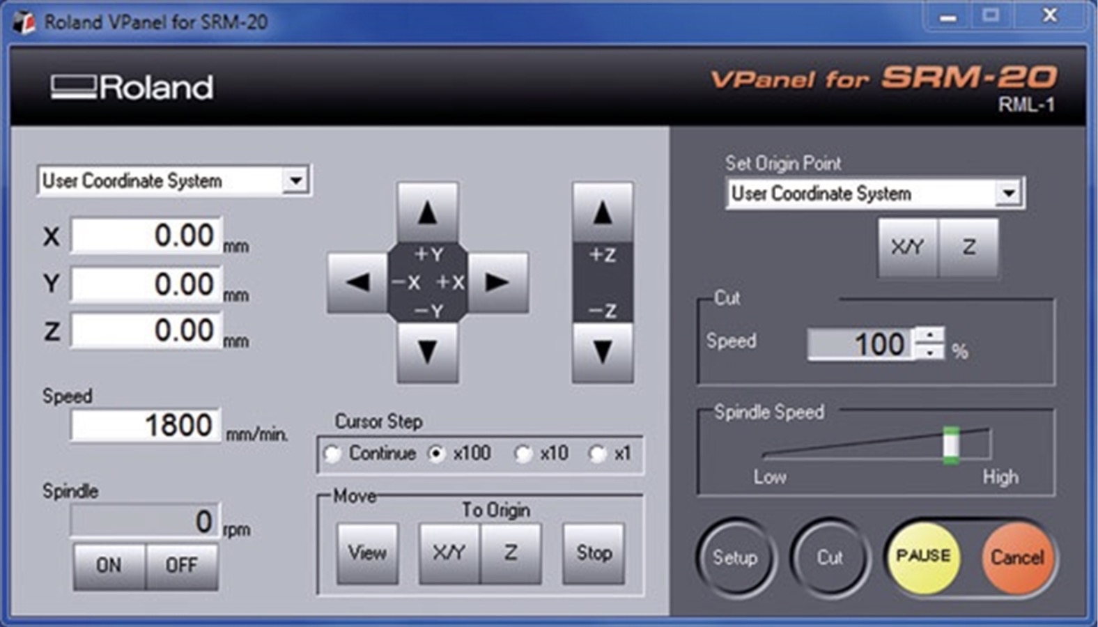
Move the X and Y position to the bottom left of your copper board.
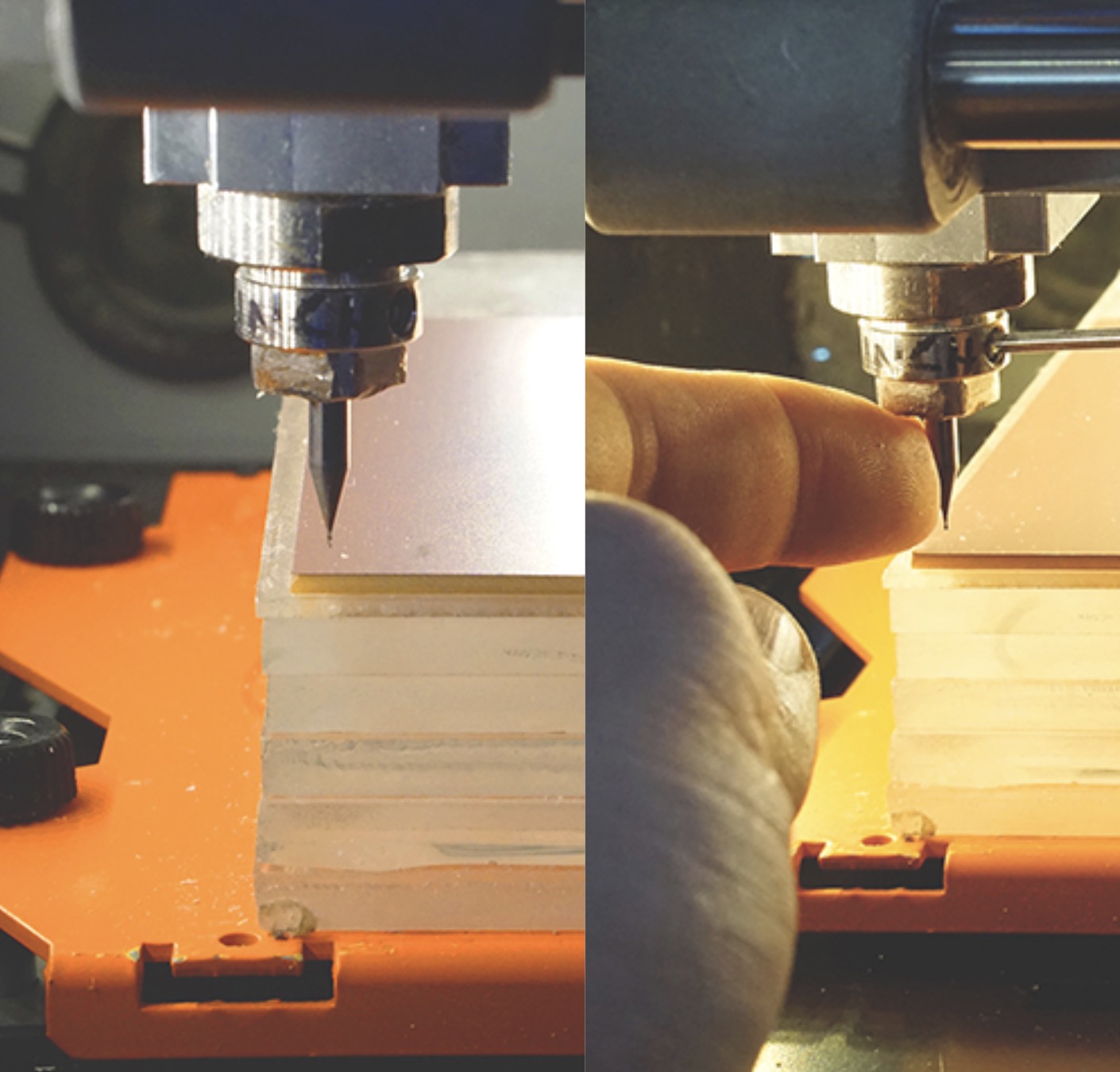
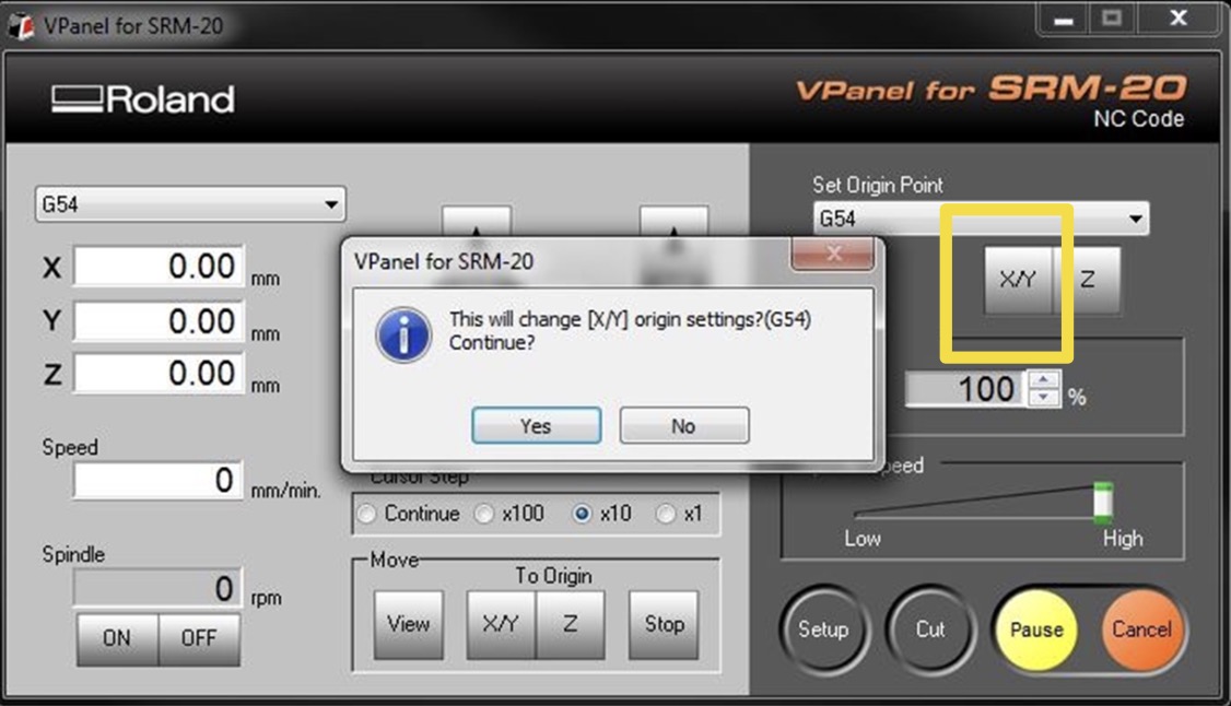
Set this coordinates as your X and Y origin.
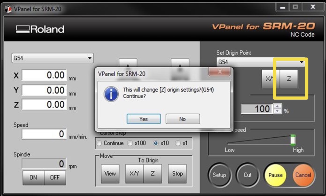
Now release the clamping screw and manually guide the endmill down to the place. Then retighten the screw and set it as the origin of your Z.
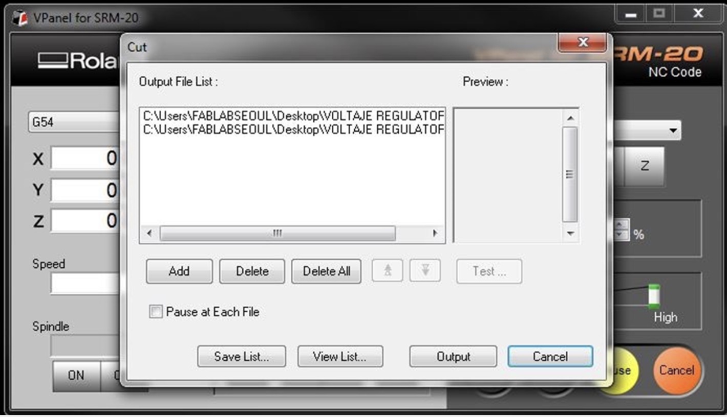
Load your files by clicking on Cut, and then select Output to the have the Roland rolling. Ha!
This is how my board came out!
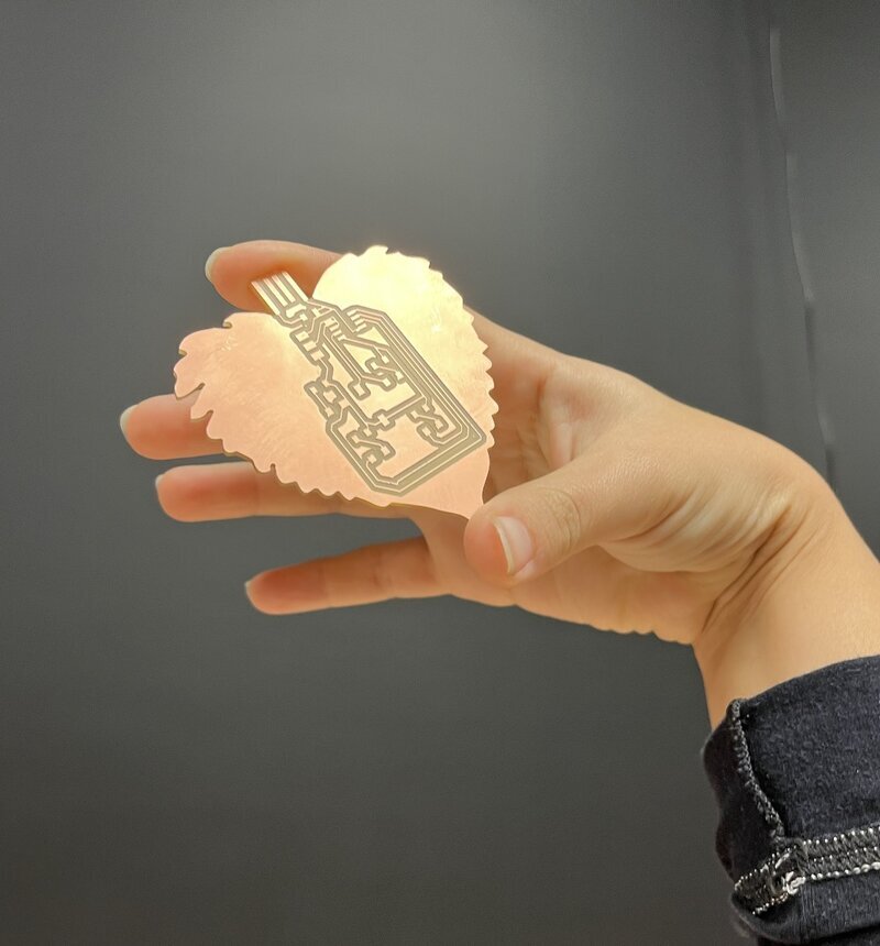
Yipiiii!!....? Actually, no time to celebrate. I had mistakes that forced me to make a new design. Clearence wasn't big enough and the mill could not go through certain places. Also, the outline shape wouldn't allow the USB to go plug in properly.
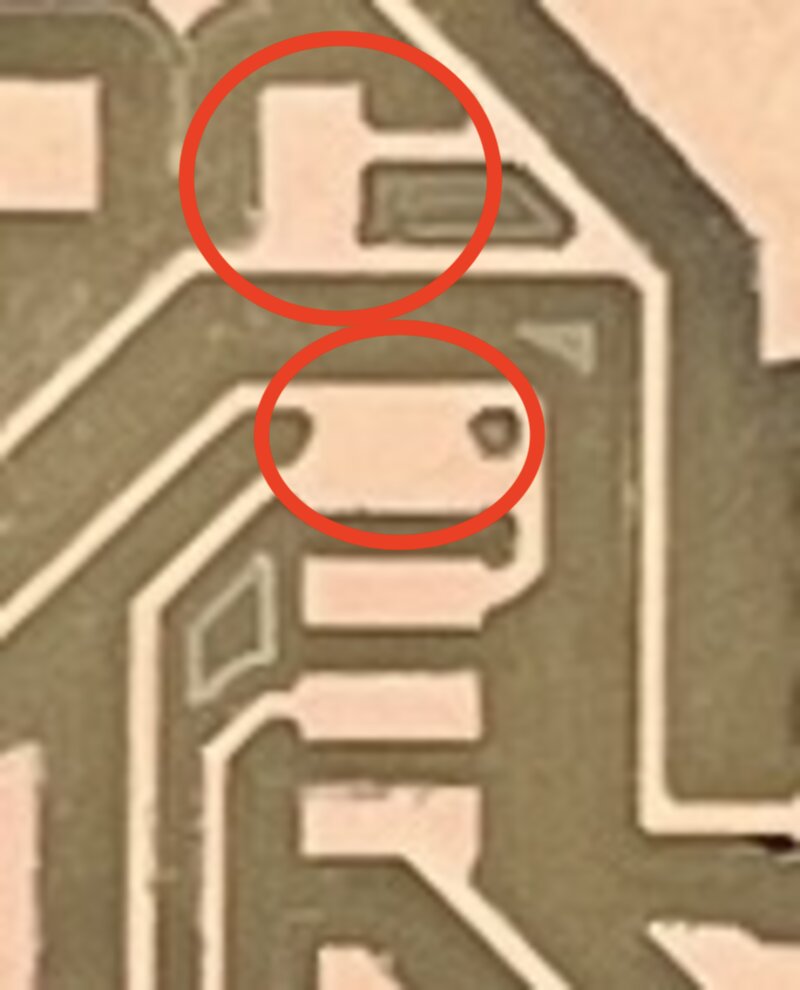
... (╯°□°)╯︵ ┻━┻
Back to the drawing board.
What went wrong, and how can I learn from this?
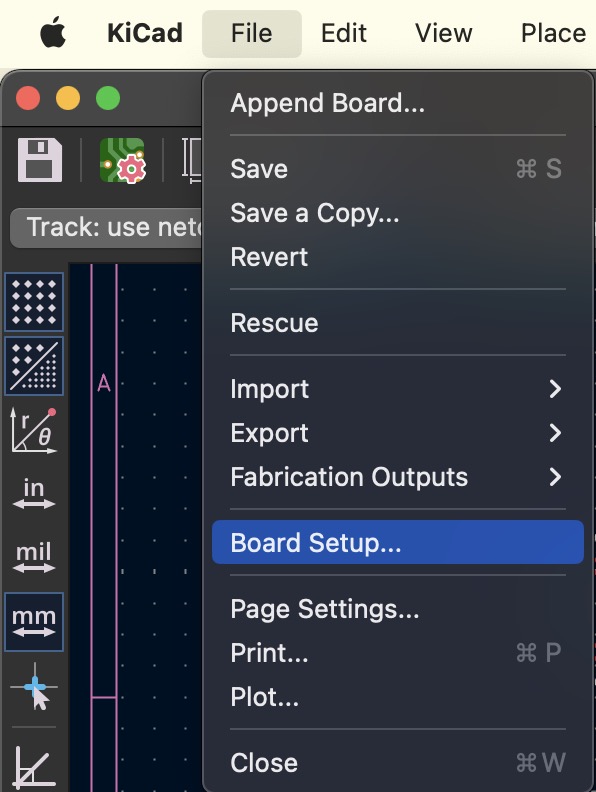
For starters, I mentioned clearence. In PCB design, clearence refers to the minimum spacing between conductive elements* (e.g., traces, pads, vias to prevent short circuits and ensure proper insulation. To set this on KiCad, go to your PCB Editor > File > Board Setup > Net Classes.
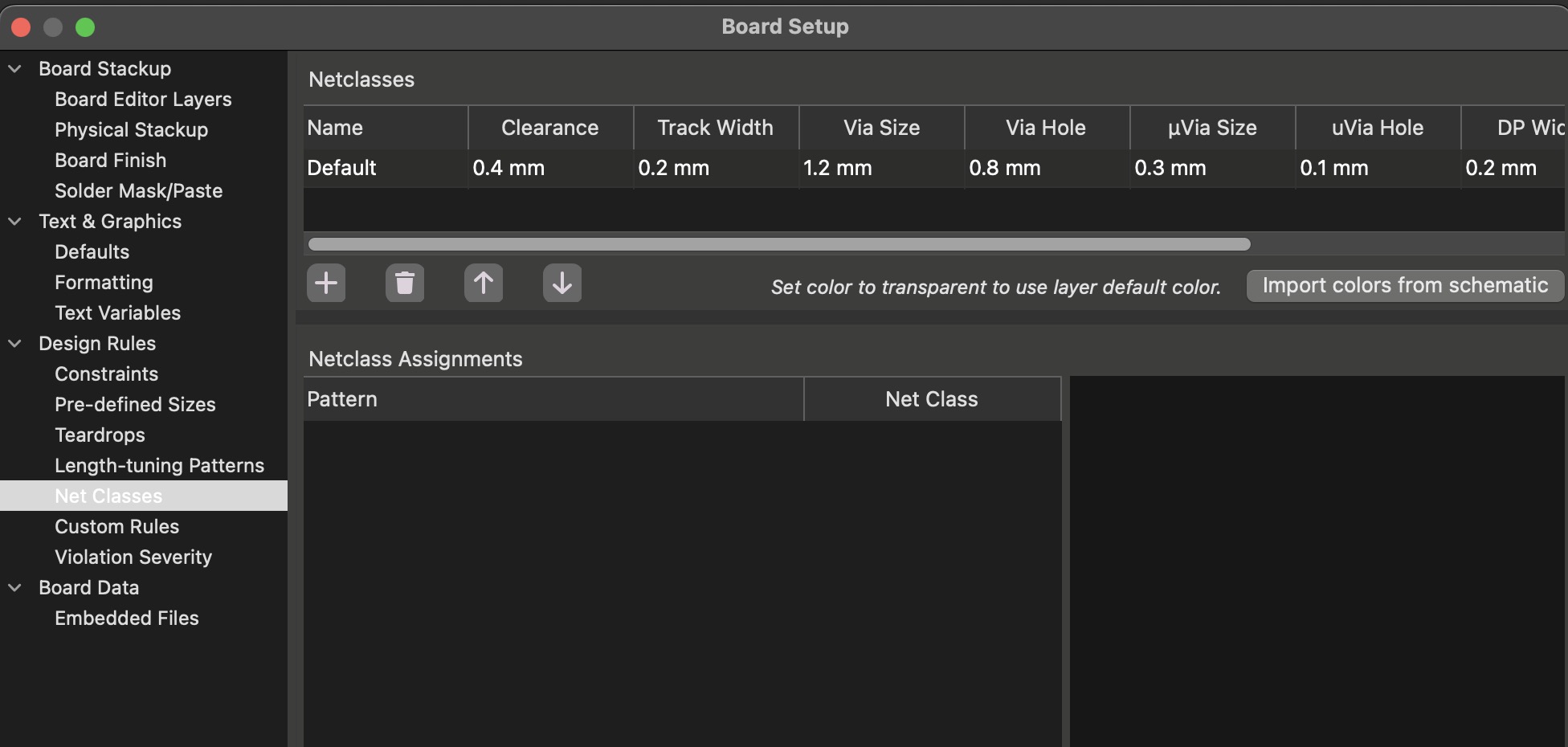
I chose 0.4mm because since I’m using a 1/64-inch (≈0.4mm) end mill for traces, setting this clearence ensures that the milling tool can accurately carve out the spaces between traces without unintended overlaps or cutting errors.
With this setup, production should go smoothly.
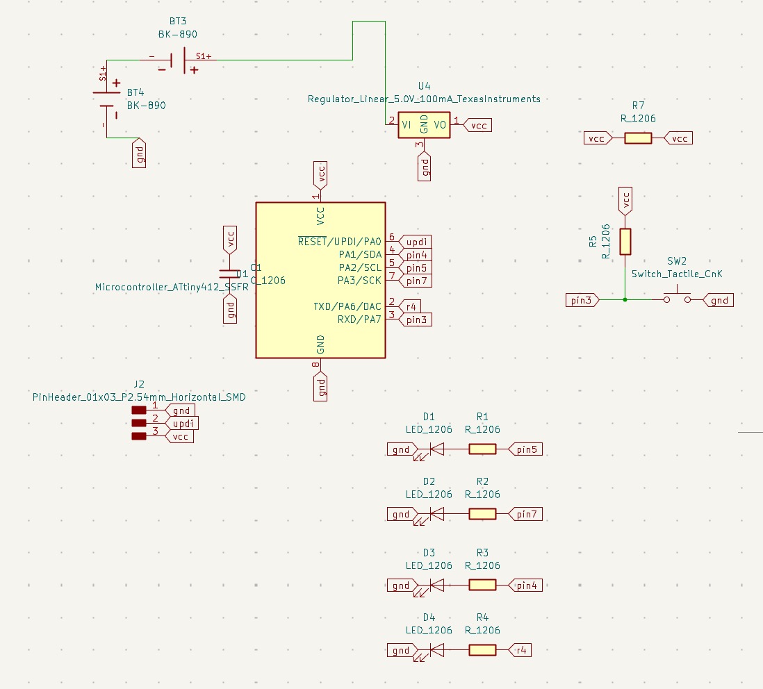
This time, I’m designing a portable version of my board while keeping the same components: 4 LEDs, 4 resistors, 1 capacitor, an ATtiny412, a UPDI for programming, and a switch button. However, instead of a standard power supply, I’ll be using two 3V button batteries.
To make this work, I need a transistor to regulate the voltage from 6V down to 5V, ensuring it’s within the ATtiny412’s operating range. Also, I’ll include two coin cell holder I found in the lab to secure the batteries in place.
This is how my schematic turned out.
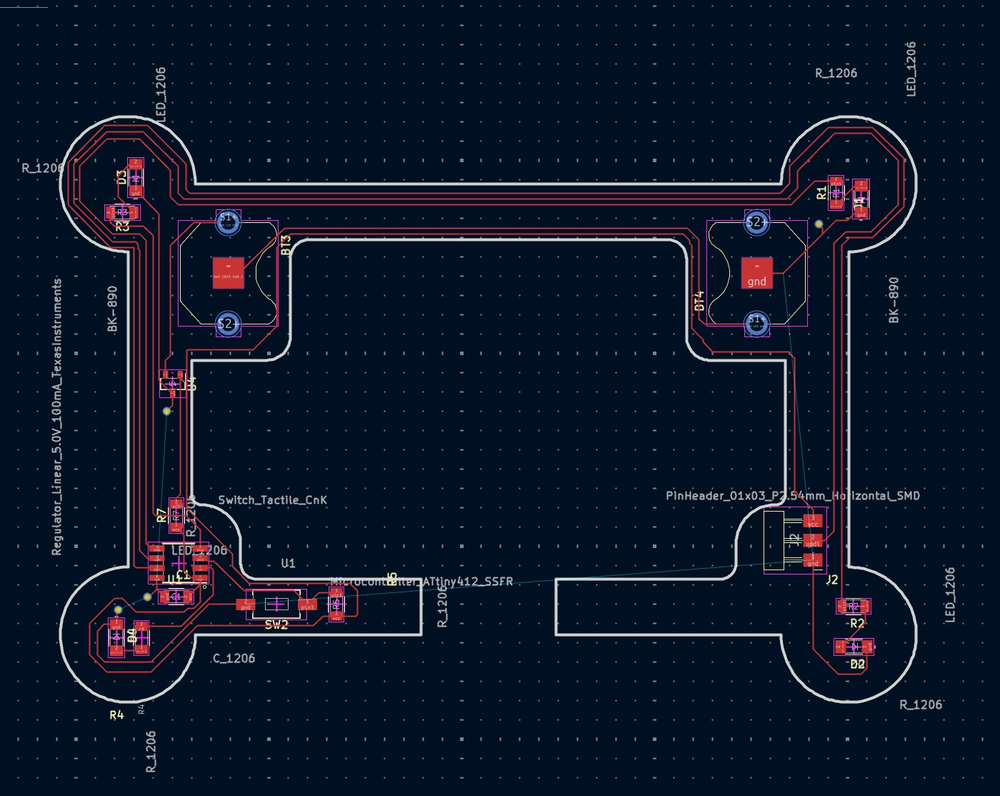
As promissed during week 6, I picked a funny shape for the outline, forcing my connections -or wiring- to get a little weird.
The goal is to assemble the PCB into a resin sculpture, so I exported the 3D model from KiCad into Blender to see how it would turn out.
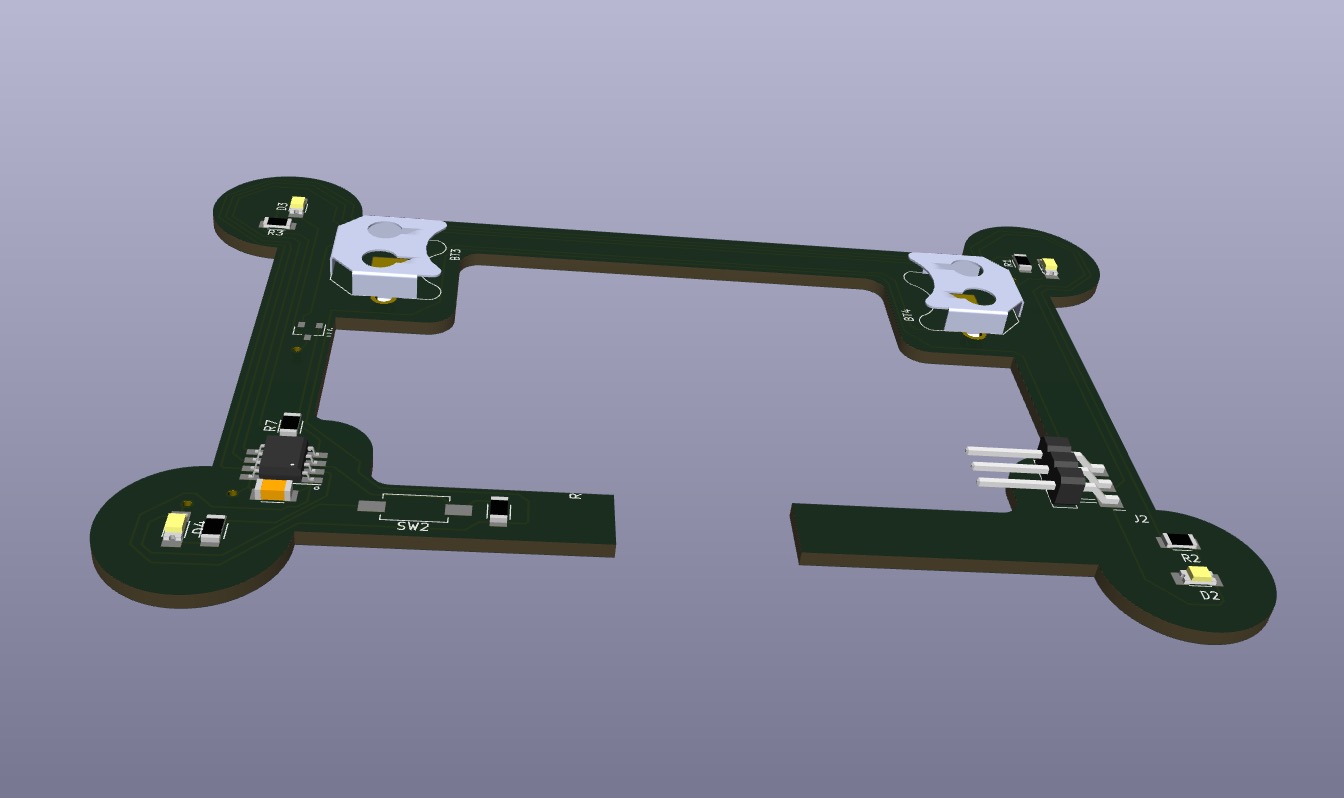
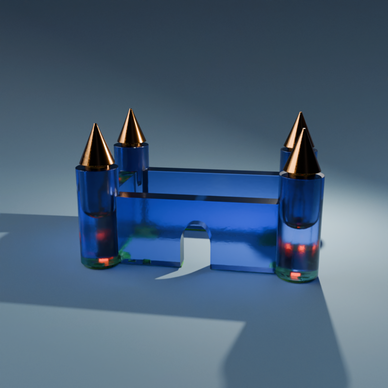
Beautiful (๑>ᴗ<๑).
You can see how this project progressed as I continue it throught week 9 and see its results week 10.