Electronics Design
Group assignment
For the group assignment for electronics design. The task involves using test equipment to analyze a microcontroller circuit board. This includes using a multimeter and an oscilloscope.
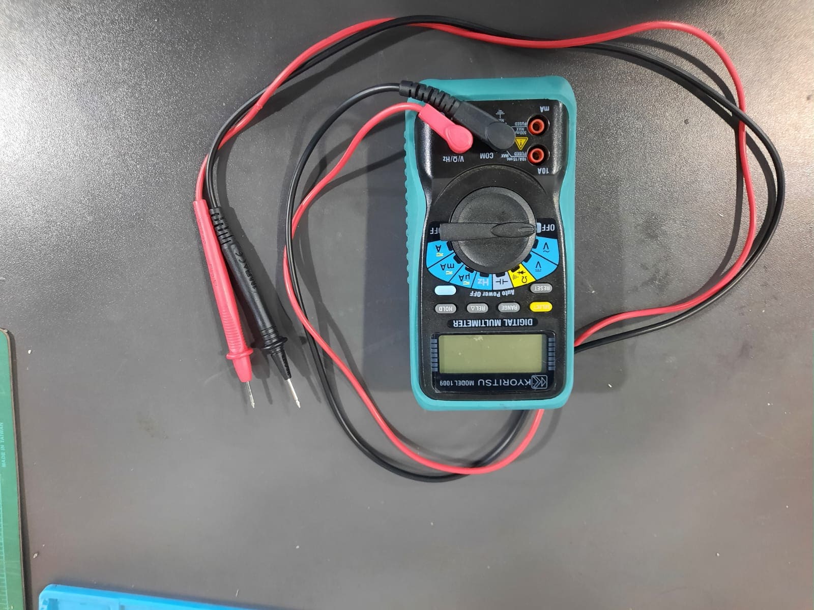
A multimeter is a versatile tool that measures various electrical properties like voltage, current, and resistance. It features a display, a function selection dial for choosing measurement modes, a range selection dial for adjusting accuracy, and probes for connecting to circuits.
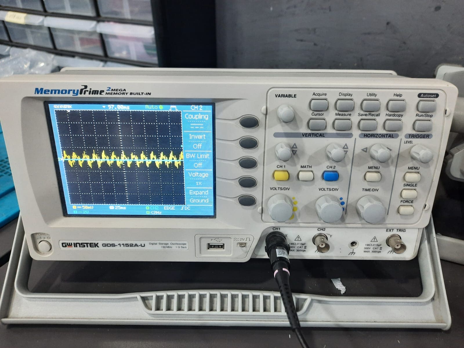
An oscilloscope is another key tool used to analyze and visualize electronic signals. It has a display, multiple channels for viewing various signals simultaneously, bandwidth limitations for the highest frequency it can capture, a sampling rate that determines how often it measures the signal, and controls for adjusting the scale and position of waveforms on the display.
The assignment requires using the multimeter to measure voltage levels at different points on the circuit board, including the sensor. The oscilloscope will then be used to observe how the sensor's voltage output changes.
Compared to the multimeter, the oscilloscope offers a more detailed and real-time visualization of voltage changes. It's also faster at capturing rapid voltage fluctuations.
The assignment goes on to use the oscilloscope to observe the signal going to the LED when the microcontroller board is programmed to make it blink on and off.
Finally, we used the oscilloscope to observe the voltage modulation and the PWM signal when they program the LED to fade on and off using PWM (Pulse Width Modulation).
Individual assignment
This individual project marks my initiation into the realm of electronics design, commencing with the establishment of KiCad and advancing through sequential stages of schematic design, PCB layout, fabrication, and testing. This documentation provides a comprehensive account of the systematic approach undertaken to develop and prototype a bespoke PCB.
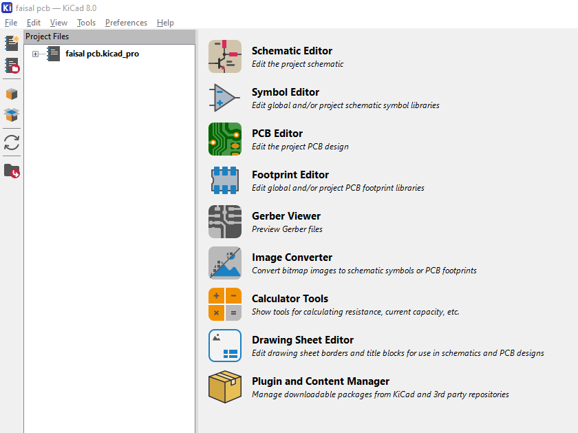
I started by downloading and installing KiCad, an open-source suite for electronics design automation. Furthermore, I added the Fab library to my KiCad setup, granting access to a diverse array of component footprints essential for my project.
Initiating the Project:To commence the design process, I created a new project within KiCad.
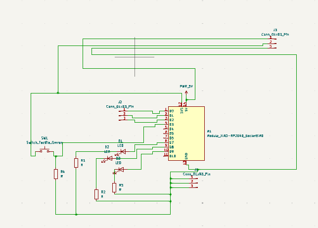
Schematic Design:Component Insertion: Utilizing the component library, I incorporated all essential components onto the schematic diagram.
I configured the connections between components to create the intended circuitry.
Moving from schematic design to PCB Editor, I began translating the schematic into a physical layout.
Components and connections were imported from the schematic into the PCB layout.
Strategically arranging components on the PCB layout allowed for optimized space utilization and maintained signal integrity.
Establishing electrical connections between components was achieved by routing traces while adhering to design constraints.
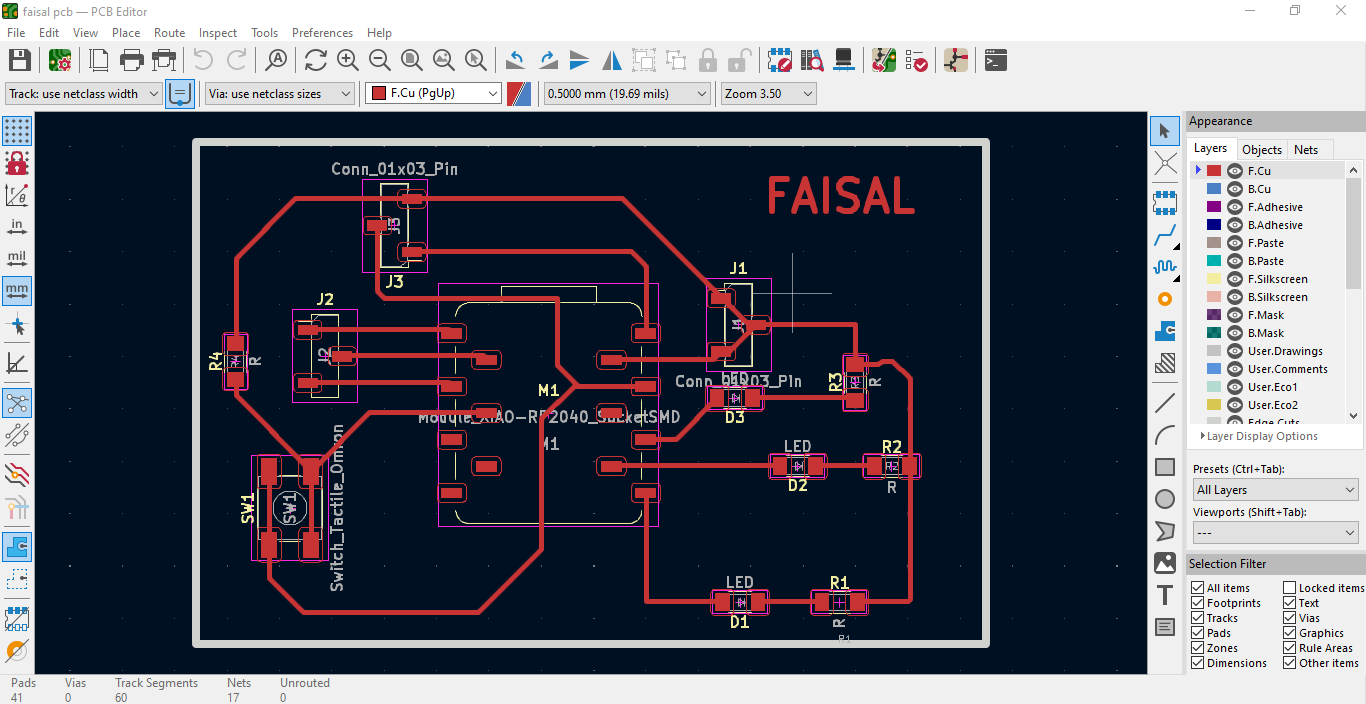
Board Constraints Definition:I've established precise constraints for the PCB layout to guarantee both manufacturability and functionality:
Minimum Track Separation: Enforced at a minimum of 0.4mm to mitigate signal interference effectively.
Minimum Track Width: Tracks have been configured to be no less than 0.45mm wide to sufficiently accommodate current demands.
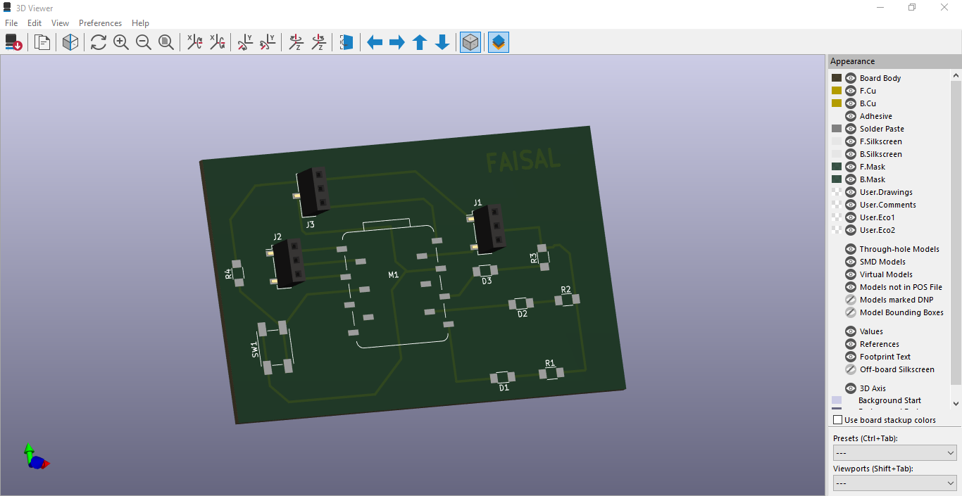
I meticulously verified the PCB layout to identify any errors or omissions. Moreover, I employed the 3D visualization tool to confirm the positioning of components and guarantee adequate clearance.
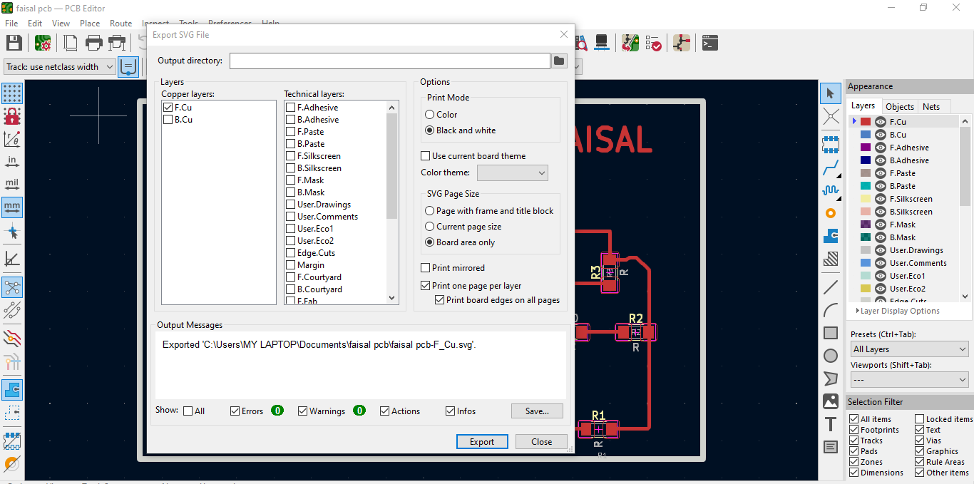
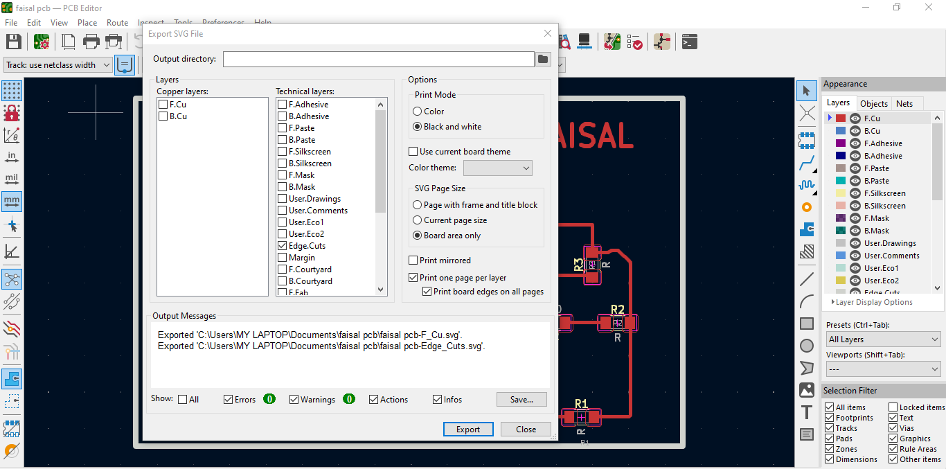
Exporting PCB Files:To facilitate further processing, I exported SVG files encompassing traces, drills, and outlines from KiCad.
First I export the traces layer as shown
Then I export the file for the outlines as shown
Creating Toolpaths
For further steps how to set the design n Mods project and downlod it to the machine see Electronics production week.
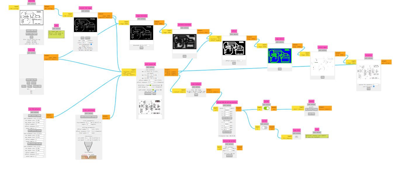
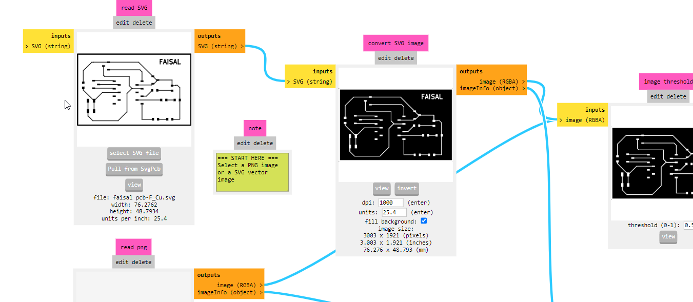
I created toolpaths using Mods software to ensure precise PCB milling.
I began the process of PCB fabrication by milling the board using the toolpaths generated, meticulously ensuring that each step adhered to the design specifications with precision.
The completed PCB underwent thorough testing to verify its performance and reliability and ofcourse after I solder the component
Button and LED Toggle Code for Seeed XIAO RP2040 in Arduino IDE
Overview
This documentation provides a detailed explanation of a simple Arduino program that toggles three LEDs on and off using a button. The code is designed to run on the Seeed XIAO RP2040 microcontroller. When the button is pressed, all three LEDs change their state from ON to OFF or vice versa.
Components Required
- Seeed XIAO RP2040
- 3 LEDs
- 3 Current-limiting resistors (220 ohms recommended)
- 1 Push button
- PCB and soldering tools
Pin Configuration
- Button: Connected to digital pin 4 (
buttonPin). - LED 1: Connected to digital pin 7 (
ledPin1). - LED 2: Connected to digital pin 8 (
ledPin2). - LED 3: Connected to digital pin 9 (
ledPin3).
Circuit Diagram
Connect the components as shown in the following table:
| Component | XIAO RP2040 Pin |
|---|---|
| Button | D4 (digital pin 4) |
| LED 1 | D7 (digital pin 7) |
| LED 2 | D8 (digital pin 8) |
| LED 3 | D9 (digital pin 9) |
The button should be connected between the digital pin 4 and ground. Each LED should be connected to its respective pin with a current-limiting resistor between the pin and the LED anode. The cathode of each LED should be connected to ground.
Soldering Instructions
Prepare the PCB: Place the Seeed XIAO RP2040, LEDs, resistors, and push button on the PCB according to the pin configuration table.
Solder the Components: Carefully solder each component to the PCB. Ensure that the connections are secure and that there are no short circuits.
Check Connections: Use a multimeter to verify that all connections are correctly made and that there are no shorts.
Code Explanation
Variable Definitions:
buttonPin: Pin number for the button.ledPin1,ledPin2,ledPin3: Pin numbers for the LEDs.buttonState: Current state of the button.lastButtonState: Previous state of the button.
Setup Function:
- Initializes LED pins as OUTPUT.
- Initializes the button pin as INPUT.
Loop Function:
- Reads the current state of the button.
- Checks if the button was pressed (transition from HIGH to LOW).
- Toggles the state of the LEDs when the button is pressed.
- Updates the last button state.
- Adds a delay to debounce the button and avoid multiple toggles on a single press.
Code
cpp// Define the pins for buttons and LEDs
const int buttonPin = 4;
const int ledPin1 = 7;
const int ledPin2 = 8;
const int ledPin3 = 9;
// Variables to store the state of buttons
int buttonState = 0;
int lastButtonState = 0;
void setup() {
// Initialize the LED pins as outputs
pinMode(ledPin1, OUTPUT);
pinMode(ledPin2, OUTPUT);
pinMode(ledPin3, OUTPUT);
// Initialize the button pin as input
pinMode(buttonPin, INPUT);
}
void loop() {
// Read the state of the button
buttonState = digitalRead(buttonPin);
// Check if the button is pressed (active LOW)
if (buttonState == LOW && lastButtonState == HIGH) {
// Toggle the LEDs
digitalWrite(ledPin1, !digitalRead(ledPin1)); // Toggle LED 1
digitalWrite(ledPin2, !digitalRead(ledPin2)); // Toggle LED 2
digitalWrite(ledPin3, !digitalRead(ledPin3)); // Toggle LED 3
}
// Save the current button state for the next loop iteration
lastButtonState = buttonState;
// Add a small delay to debounce the button
delay(50);
}
Steps to Upload the Code
Install the Arduino IDE:
- Download and install the Arduino IDE from the official Arduino website.
Add Seeed XIAO RP2040 Board:
- Open the Arduino IDE.
- Go to
File > Preferences. - In the "Additional Board Manager URLs" field, add the following URL:ruby
https://github.com/earlephilhower/arduino-pico/releases/download/global/package_rp2040_index.json - Click
OK. - Go to
Tools > Board > Board Manager. - Search for "Raspberry Pi Pico" and install it.
- After installation, go to
Tools > Boardand selectSeeed XIAO RP2040.
Select the Board and Port:
- Go to
Tools > Boardand selectSeeed XIAO RP2040. - Go to
Tools > Portand select the appropriate port for your XIAO RP2040.
- Go to
Upload the Code:
- Copy and paste the provided code into the Arduino IDE.
- Click the
Uploadbutton to upload the code to the XIAO RP2040.
Usage
Once the code is uploaded, pressing the button will toggle the state of the three LEDs. Each press will switch the LEDs from their current state (ON/OFF) to the opposite state.
Troubleshooting
- Ensure all connections are secure.
- Verify that the correct board and port are selected in the Arduino IDE.
- Check the button and LED wiring for proper connections.
- Make sure the current-limiting resistors are in place to prevent damage to the LEDs.
This simple project provides a foundation for understanding basic input and output operations on the Seeed XIAO RP2040 and can be expanded for more complex applications.