8. Electronics design
Group Assignment
This week our instructor OniK taught us a lot about electronics.
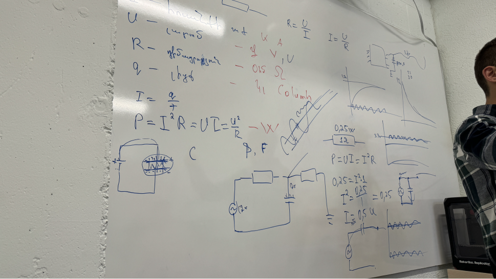
And I finally learned about protocols and different types of pinmods.
PWM - The process of power control by pulsating switching on and off energy consumers. It us only one pin and devices (out or in) understand this signal in one period time how long it high or low .
UART(Universal asynchronous receiver/transmitter)- It has minimum 3 contacts RX ,TX and GND. The transmitting line is TXD (Transmitted Data), and the RXD (Received Data) port is receiving. To decrypt the signal, the device uses pre-set bitrates, which fragment the signal into 0 and 1 per unit of time; therefore, to properly work, you need to correctly determine the bitrate (4800, 9600, 19200, 38400, 57600, 115200, 230400, 460800, 921600). Bitrate also affects the data transfer speed.
I²C (Inter-Integrated Circuit) - Uses two bidirectional communication lines (SDA and SCL). I2C is synchronous, consists of two lines: data (SDA) and clock (SCL). There is a manager (primary) and a managed (secondary). The initiator of the exchange is always the primary; no exchange is possible between two secondary. In total, there can be up to 127 devices on one two-wire bus. To decrypt the signal, the device uses the bitrates seted by the main device sing scl (clock) pin.
SPI (Serial Peripheral Interface)- has 4 pins SPI is a synchronous interface in which any transmission is synchronized to a common clock signal generated by the main device (processor). The receiving (secondary) peripheral synchronizes the receipt of the bit sequence with the clock signal. Multiple chips can be connected to one serial peripheral interface of a chip main. The main selects the secondary to transmit by activating the chip select signal on the secondary chip.
- MOSI - main output, secondary input. Serves to transfer data from the main device to the secondary.
- MISO - main input, secondary output Used to transmit data from the main device.
- SCL - is a sequential Serial Clock. Serves to transmit a clock signal to secondary devices.
- CS or SS - chip selection, secondary selection
 This week we also created logic analyzer using Arduino and read the I²C signal from my microcontroller to the LCD display.
This group activity turned out to be very productive as I began to understand how electronics work and how current turns into zeros and ones.
Individual assignment
This week we will finally learn how to design an PCB. And use EDA programs, specifically KiCad. So first of all I did a little research on the components and how they work. Then I started designing in KiCad.
PCB Design
I already installed KiCAD in previous classes, but this week I also installed the FAB Academy library.
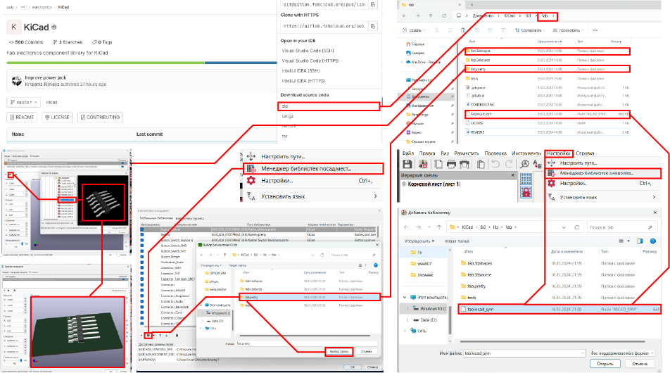
After installation I started designing my PCB.
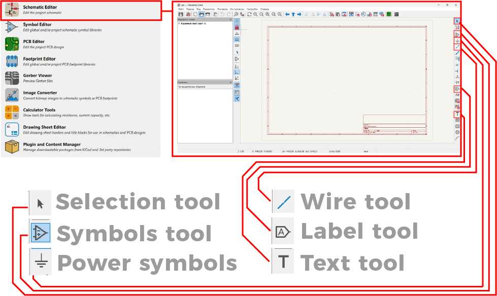
Tools that I used
Circuit Diagram
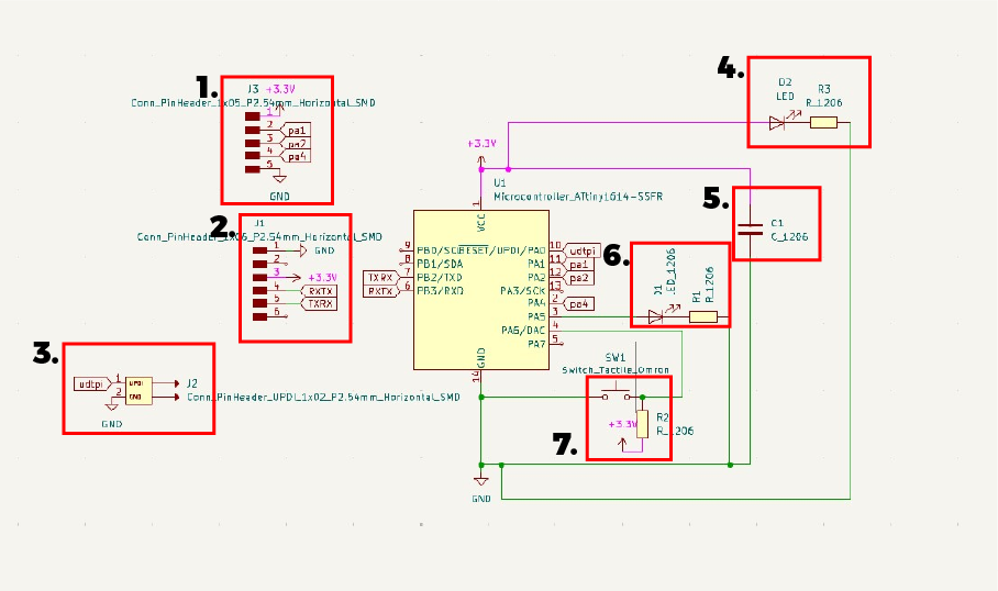
So this is my circuit diagram and I want to tell why I designed it like this.
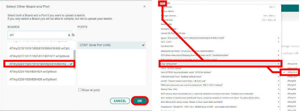
So i used ATtiny 1614 because it is the most easiest to use.
- Some free pins that I will use in the future.
- The connector on which the RX TX and GND is connected for the UART protocol, which I will use in the future.
- Connector with updi and gnd for further programming.
- Led with resistor connected directly to the power source and the gnd to indicate .
- The decoupling capacitor on the board should be located as close as possible to the chip.
- Built-in LED with its own resistor to check the functionality of the board.
PCB Editor
So after I’ve created the circuit, I click on this icon and start editing the board.

This stage was not easy because there were many intersecting paths, I went through it many times, but could not solve this problem.
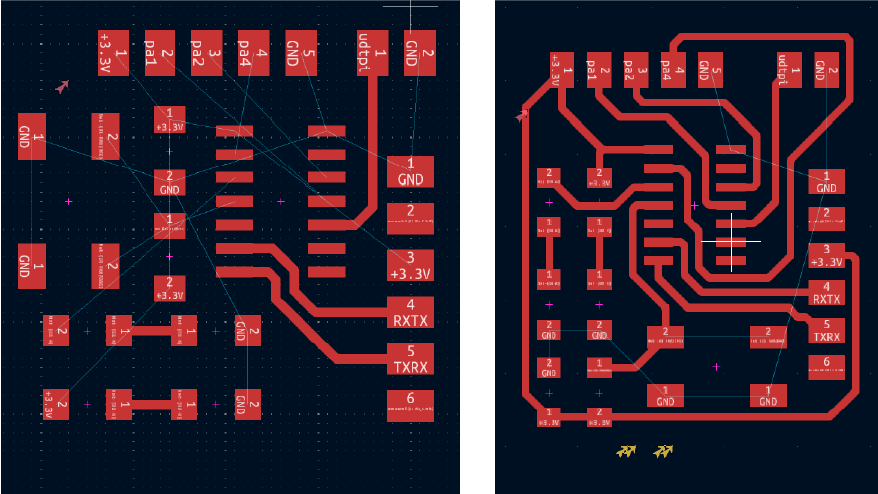
I finally solved the problem I thought I made a general grounding, but this was not enough, since some places were isolated from each other.
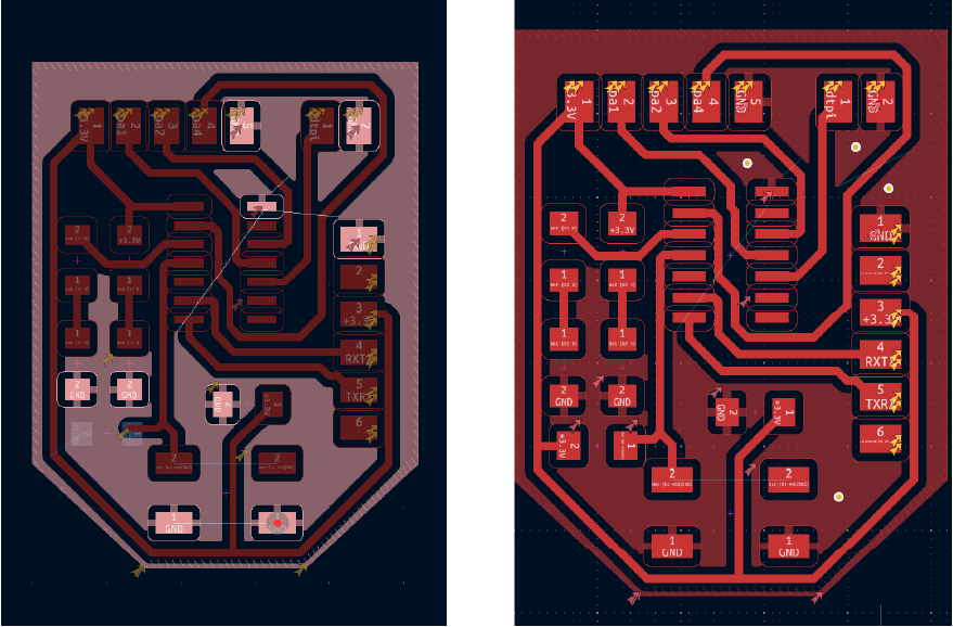
And so I decided to make holes and connect them with the back side.
Export
After that I exported it to SVG.

I exported the paths separately and the outer contours and holes together.
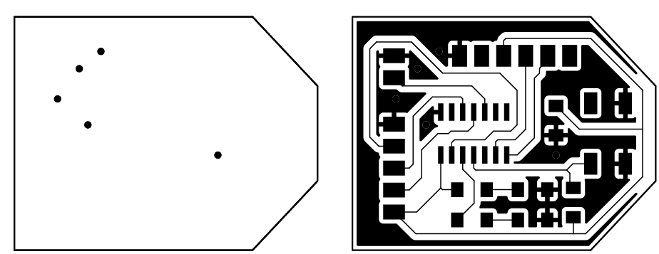
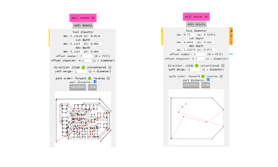
Then i generated g code in mods.
PCB Production
Unfortunately, I forgot to take photos and screenshots of PCB production, but you can see my Production week.
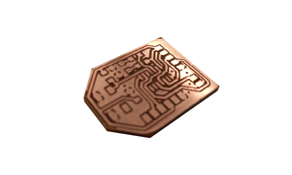
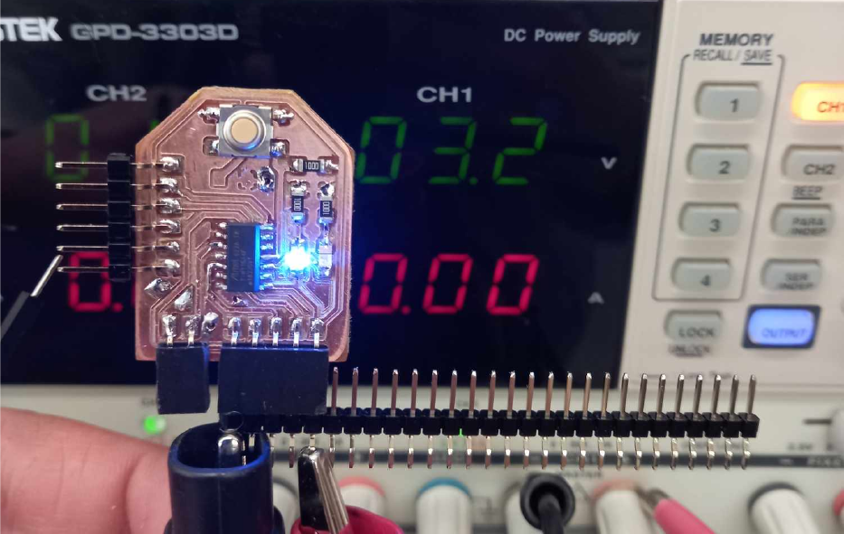
So, after I milled on Roland, did the soldering and then checked for shorts, everything was fine, I also checked the 3.3V power supply. so everything was ok .
Programing
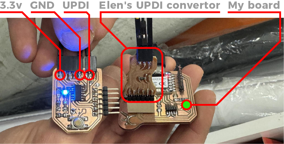
and so I used the Elen’s UPDI convertor to transform my board into a programmer. Thanks Ellen for this. And so this is how I did that.
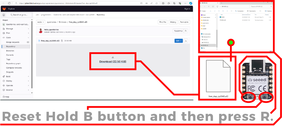
First i reseted my RP2040 microcontroller and loaded the uf2 file into it.
Then i upload ATtiny library and install MegaTinyCore.
URL | http://drazzy.com/package_drazzy.com_index.json

And selected the right board.
Then I used a simple Arduino Blink example to test my board.
/*
  Blink
*/

// the setup function runs once when you press reset or power the board
void setup() {
  // initialize digital pin LED_BUILTIN as an output.
  pinMode(1, OUTPUT);
}

// the loop function runs over and over again forever
void loop() {
  digitalWrite(1, HIGH);  // turn the LED on (HIGH is the voltage level)
  delay(1000);                      // wait for a second
  digitalWrite(1, LOW);   // turn the LED off by making the voltage LOW
  delay(1000);                      // wait for a second
}

-
Source files
Click for downloading
KIKAD
Traces and Cutout SVGs