Week 4: Electronic Production
This week, we learned how to do the PSB milling. We started by generating a toolpaths, then preparing the Roland SRM-20, and after the milling was done, soldering the finished board. This was the first week when I had multiple things go wrong (at least 3 unsuccessfully milled board), but I also learned a lot, and now I make PCBs quite often.
Group Assignment
The page describing the group assignment for this week (characterize the design rules for your in-house PCB production process) can be found here.
Preparing the files
From the electronic design week (I did the FabAcademy in the original order when the electronic design week was before the electronic production week), we got the Gerber files, ideally all layers in the single file, and optionally some drill files.
To create the toolpaths for the Roland machine, we will use the CopperCAM software which is installed on the computer next to the PCB milling machine.
When I want to make a PCB, I like to follow the Fablab Wiki page, where everything is clearly explained, just to make sure I don’t miss anything. Here, I will outline important steps and add some bits that I found interesting / useful.
1. Import the Gerber file to CopperCAM -> make sure that the edge cut is highlighted
2. In the File -> Dimensions, margin should be 1 mm, and Z thickness a little more than your board. Then go to File -> Origin, and change it to 0 and 0 (usually Y is something like 0.05 for some reason, not sure why)
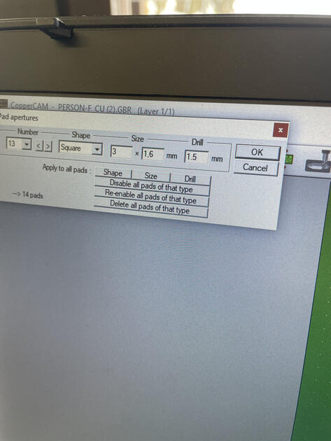
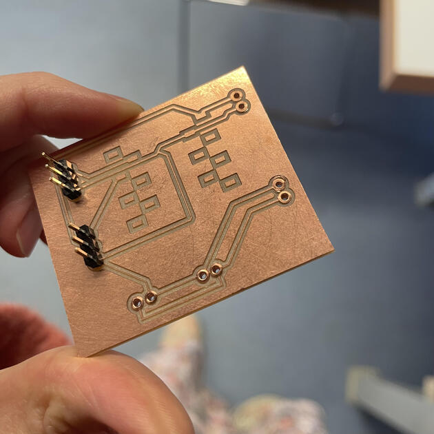
3. I usually don’t use drill files, but rather select the pad where I would like to have a hole. Then right click on it and edit it (or all identical). This will give me some options (Figure 4), one of them being “drill”. I like using rivets, so I usually make the holes bigger than rivers (for example for the 1.4 mm rivets I make the holes 1.5 mm).
There is a function using drill bit, but I made holes with 1/64 end mill in this assignment.

|
|
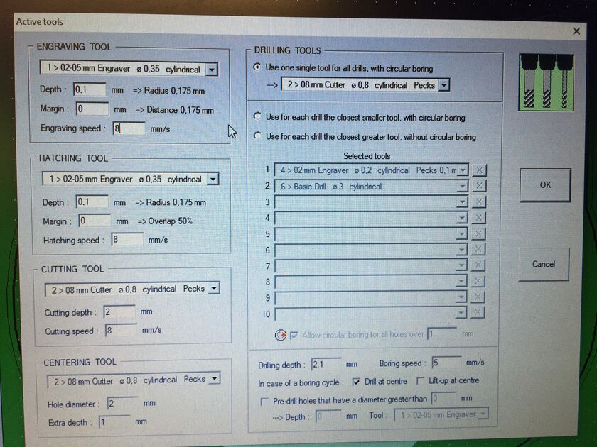
4. The next thing is to set up the tools we use. I just go with the defaults, e.g. what is written in the Wiki. There are three types on tools
- Engraving (for making the paths)
- Cutting (for cutting out the board, edge cuts)
- Drilling (for headpins or pins, min 0.8 mm diameter)
I usually only use two, one for engraving (Tool 1) and one for Drilling and Cutting (Tool 2).
5. Sometimes when I have a text in my design, at this point I right-click at one of the elements of text, and press “Engrave tacks as centerlines”. Some parts of the text might not work (for example the tilt in the letter “t” never works for me). I guess it’s ok, but then don’t forget to disable it before next step, or otherwise there will be contours around it.
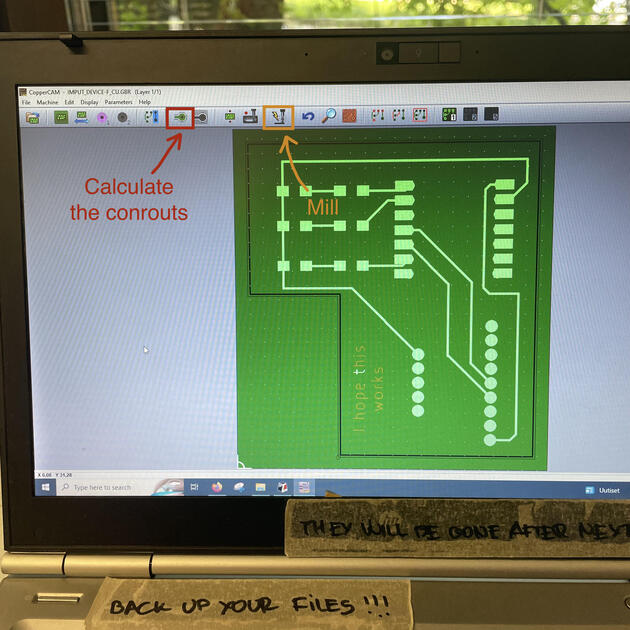
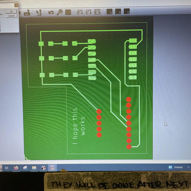
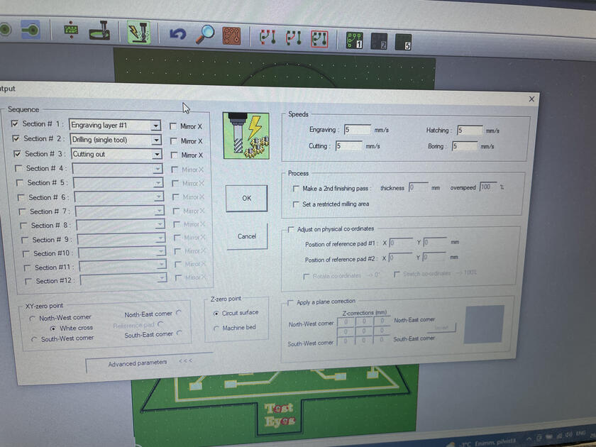
6. The next step is to calculate the contours (the button can be seen on Figure 1). There are two numbers to enter –> numbers of successive contours (how many rounds will the tip mill around the tracks and pads, usually around 3 is enough) and extra contours around pads (I usually just put 0 there).
7. The last step is to export the file. Select the Mill icon (the button can be seen on Figure 1). Engraving layer, drilling and then cutting out in this order. XY-zero should be at South west corner, and Z-zero at circuit surface. After saving, we usually get two files (named something with T(ool)1 and T(ool)2 -> one for engraving and the second one for drilling and cutting).
Preparing the Roland machine
Before we start milling, let’s prepare everything. First lets sand the copper clad a bit with the brass coil “sponge” up until its nice and shiny. We do it because (according to ChatGPT) it enhanced adhesion, removes contamination and promotes uniform coating.
The copper clad would move if we don’t attach it to the bed, so we use double-sided tape for that.
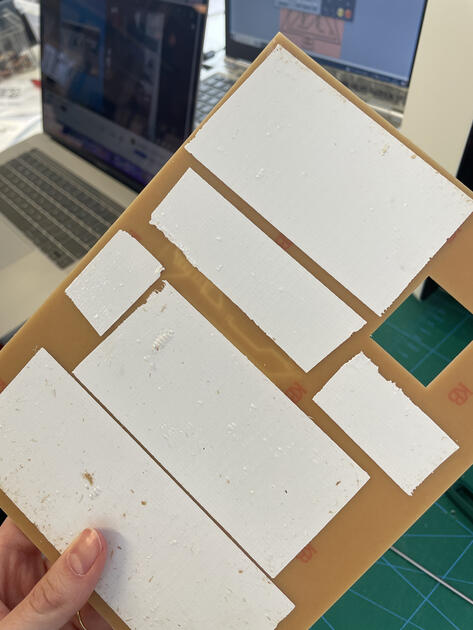
From my experience the take should cover the metal sheet evenly (not like on the Figure above), otherwise it might unstick during the print, which happened to me as well. Now I neatly tape the whole metal sheet before milling, so it sticks nicely.
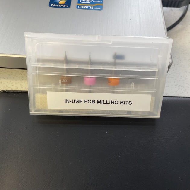
After that we should insert the correct tooltip. First engraving tip (currently it’s the brown now, as seen on Figure 6), then drilling and cutting tip (orange one on Figure 6).
The last thing to do is to set the origin point for XYZ axis. For X and Y, you can just move the tooltip where you would like the bottom left corner of your design to start, and set that as the origin in the Roland milling machine interface - make sure that there is enough space, and leave at lest 0.8 mm from edges. I usually like to go to CopperCAM and point my mouse to the top right corner of my design. Then on the bottom panel you can see the dimensions of your PCB.
Next is the setting the origin for Z-axis. The tip should be inserted all the way in, move it close to the blank PCB sheet, and stop about 5 mm from it (be careful not to touch the metal sheet as it might break the tip! There is a setting to move the tool slower). The release it and (gently) let it touch the sheet - you can then screw it back, and reset the Z-axis. I recommend setting this in the top half of your PCB design (usually in the middle, but the PCB milling machine we have the lab is a bit uneven).
Now we can start the cutting –> Cut -> delete everything -> choose your file (first tool 1, then tool 2). Sometimes you have to change to look for all files types, or it won’t find your file.
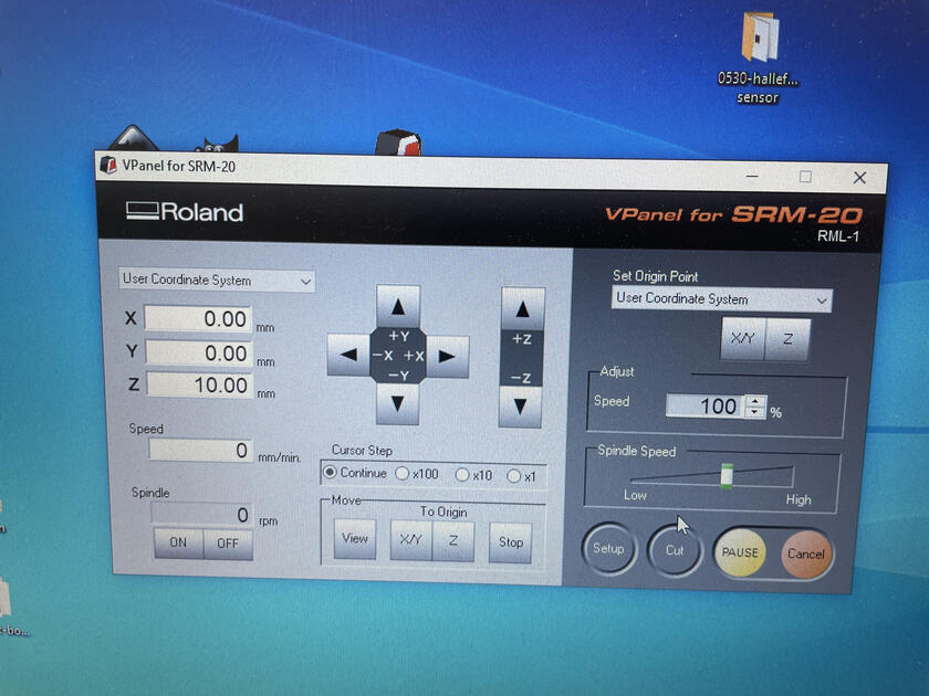
After you change the tool to do the second part of the milling (drilling and engraving), set the Z-axis origin point again, but leave the XY as it is.
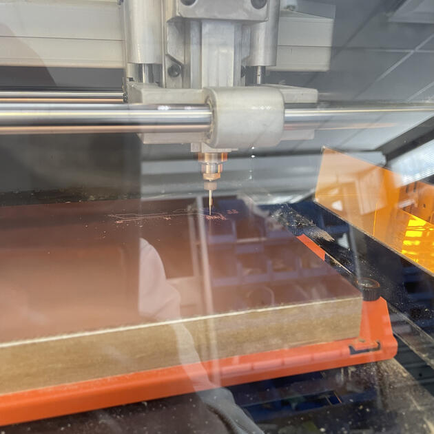
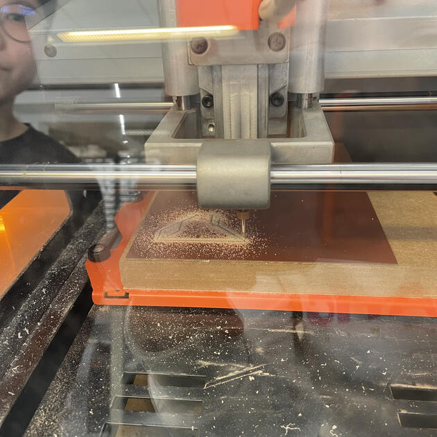
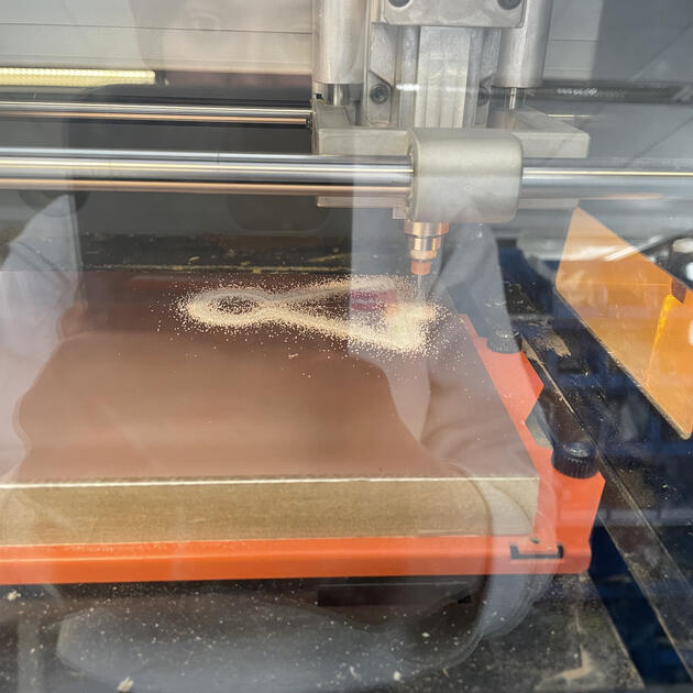
PCB Milling
Now it’s the milling time! Juts to have an estimate, it takes around 20min to mill, but depends a lot on how complicated your board is. Honestly at first I had sooo many problems with it. It was before the bed was leveled again (after I returned I didn’t have that many problems). The first mill was too shallow, and then the second one too deep.
|
|
The two videos bellow: in the right one the cut is too shallow, and therefore if fails to scrape the conductive layer (everything is then connected to everything). In the left video I think the cut is too deep (and I perhaps had a wrong file where the traces were too thin, not 0.4 mm as we are supposed to be set up in the KiCAD, but the default 0.2 mm), and there were no traces between some components.
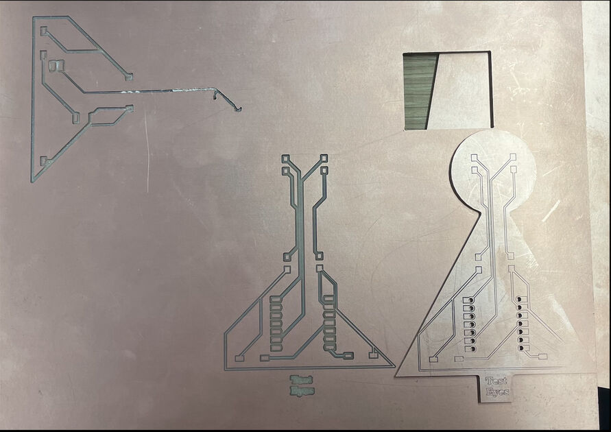
At the end of the day, I managed to get some working PCBs. The ideal scenario is that the traces are connecting only the components they are supposed to be connecting. There were two big learning:
- the top right corner of the bed works the best, the rest is quite troublesome
- for bigger PCBs use the bigger CNC machine
Other problem
When we run out of singe sided sheets, I just used the double-sided one, and put holes for rivers in it - big mistake!. Had to scrape it, and even then it worked meh. Need to be more careful next time.
Soldering and Testing
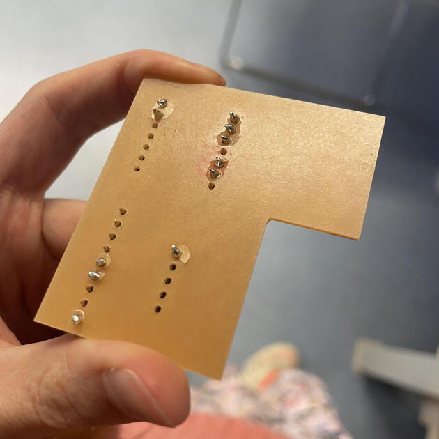
The multimeter became my best friend - checking whether my soldering works, whether there is a short circuit etc. I also started to like the rivets - connecting the top of the board with bottom, or just soldering it on the bottom. Honestly though, it also happened that many times they did not work as expected. Then I however learned that you should connect the top of rivet to the trace with a little of solder, to make sure that they are indeed connected.

|
|
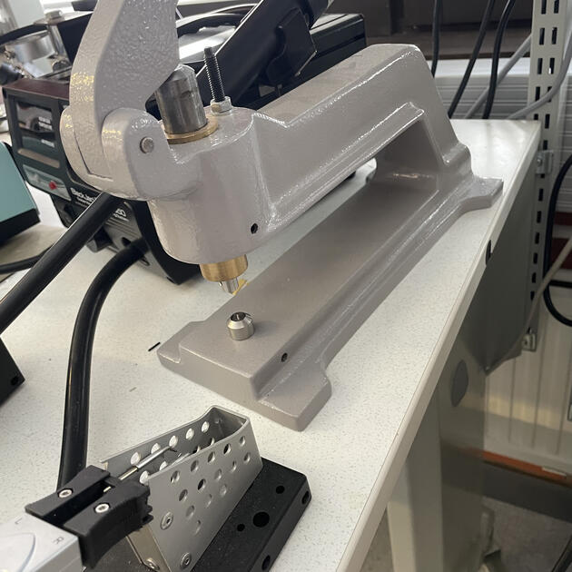
There is also a two-sided rivet punch tools (used with hammer).
|
|
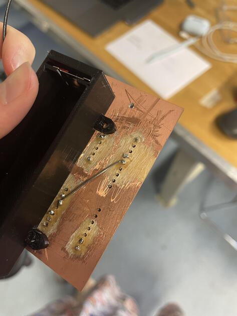
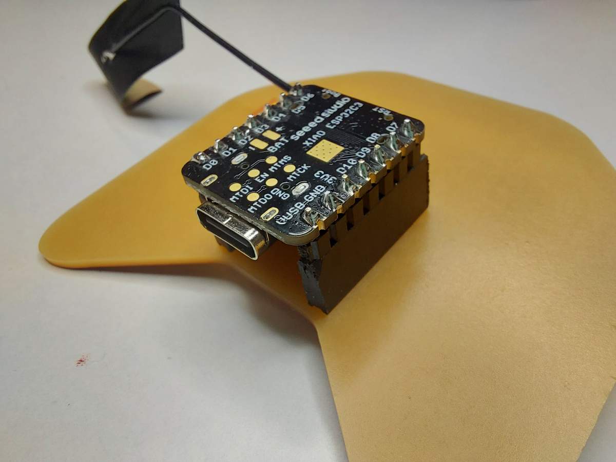
Then I saw that Saskia did –> she put the XIAO from the bottom, and soldered it on top (Figure 20). Of course one needs to be careful and mirror the pins when making the design. It looked quite nice, and easy to solder. I should try that the next time.
I also learned a lot about soldering, especially about soldering tiny components. During my first try, I wanted to make everything at once, and then I expected it would work just like that. But it’s not that not simple, and it is also impossible to debug afterwards. I learned my lesson when I was looking for my mistake (short circuit) for solid 20 min. I even removed the component (Figure 21).

|

|
What I do now (in addition to soldering one pad at a time) is that I put a bit of solder to a pad fist. Then I put some component on top of it, using tweezers. Now when I meld the solder, the component will just nicely sink in to it and hold perfectly.
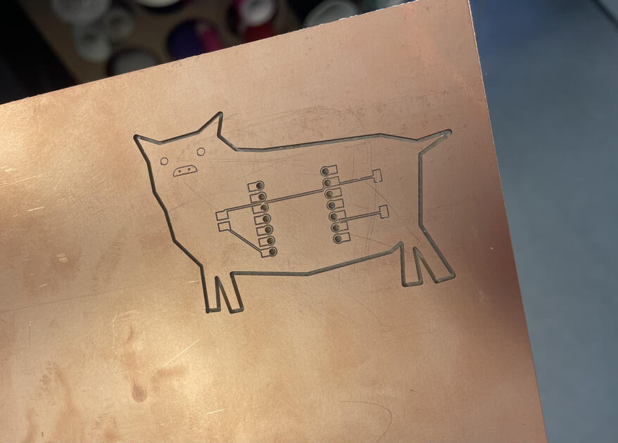
Final boards
During this week, I made a few boards, and the first one were quite unsuccessful. But then I learned a lot from it, and then made a good boards, such as “The pig” and “Tiltmeter” - more about this (also a code for it) can be found in my Week 11 documentation.
Files
- The KiCAD files for tiltmeter - [Download]
- KiCAD of the pig - [Download]
- KiCAD of the “person” - [Download]