Week 8: Electronic Design
This week we were working on Electronic design - PCB design. PCB stands for Printed Circuit Board, and it is a board that connects electronic components and provides a pathway for electrical signals to travel between them. It can be very useful to make a custom PCB for a specific project, as this can save space and there won’t be that many cables.
Group assignment
The page describing the group assignment for this week (using the test equipment to observe the operation of a microcontroller circuit board) can be found here.
Testing equipment in the lab
In our lab we have multimeters, power supply, oscilloscope and logic analyzers. All of them are super useful in debugging a circuit board, and provide a great insight in what’s going on in the board
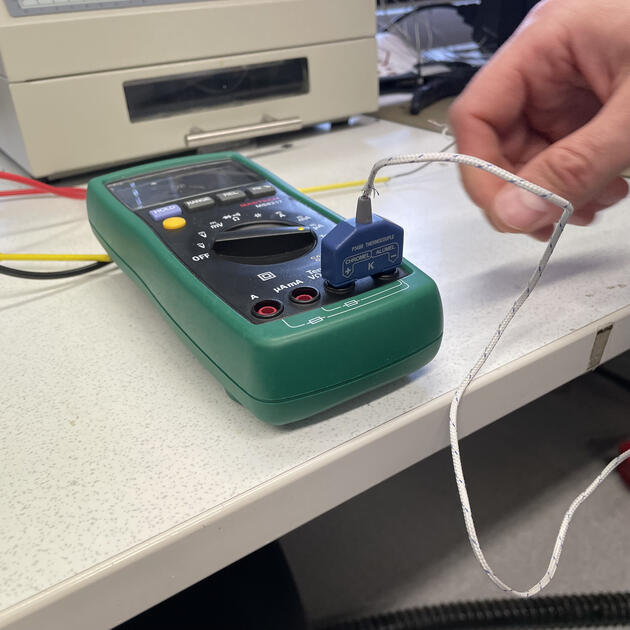
Multimeter
I used the voltmeter to find out the operating voltage of our XIAO board. It was (unsurprisingly) 3.3V.
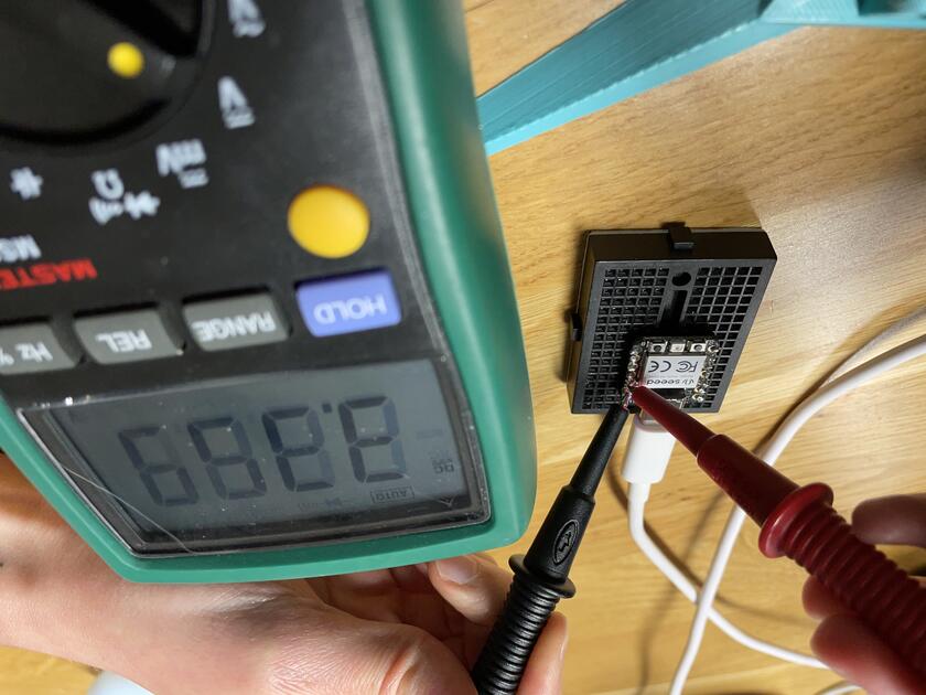
However, multimeter can be used for much more. It can measure current and voltage in a circuit. It can measure resistance and capacitance of electronic components, temperature as well. I mostly use it to detect if circuit is well-connected, and for short circuits.
Oscilloscope
We can think of oscilloscope as a multimeter, but in time. It can draw the signal changes (voltage) in time, which can be sometime very useful.

I sometimes think of is as VS Code debugger, but for hardware. When all else fails, and you still don’t know what is going on, use oscilloscope.
Power supply
I used power supply to test motors - to see what is their working voltage, and how much current they pull.

Power supply can make a specific voltage, and limit current to some maximum value. Before you turn it on, you can connect the terminals. Then when you turn it on, the voltage will be 0 (as we just made a short circuit), and we can then set the maximum current that will be flowing. After that we turn of the machine, and disconnect the terminals. Then, when we turn the power supply back ok, we can set the desired voltage.
Electronic design - KiCAD
We will use KiCAD to make the design, mainly because, there is an electronic components’ library that contains all available components in FabLab.
brew install --cask kicad
After we install KiCad, we should download the Fab KiCad library. Then run KiCad and go to “Preferences/Manage Symbol Libraries” and add fab.kicad_sym as symbol library. Similarly, go to “Preferences / Manage Footprint Libraries” and add fab.pretty as footprint library.
KiCAD Schematic Editor
The first step in designing a PCB is a schematic design. So from the KiCAD menu, we should start a new project and open a “Schematic editor”.
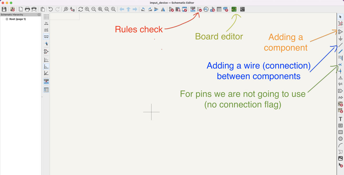
In the figure above I tried to note the most crucial buttons for a schematic design - there is much more functionality there that can be useful and helpful, but this should be enough for a simple design.
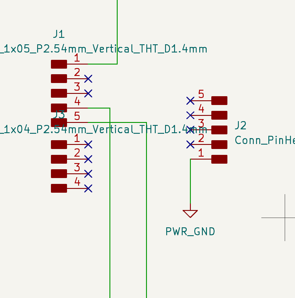
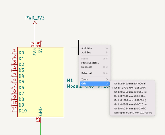
Step 1: Add the components we want to use. We should add them from the fab symbols library, so we know it’s the ones we have at the lab.
Note! - some components are not present in the symbols’ library, but some of them can be just added to the board on pin headers. Look for different size pin headers in the symbols (we can even combine them together). In the schematic design the scale doesn’t matter that much, but in PCB design make sure that the pins are a multiple of 2.54 mm (0.1in) apart -> change the grid to help you with that.

|
|
Step 2: Connect them according to your design (with “add a wire” button).
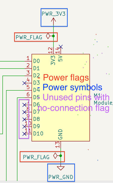
Step 3: Add power (3v3 and Ground, or whatever your design needs). Add power flags. The power flags are special symbols telling ERC where power comes from.
Step 4: Add a no-connection flag to unused pins. It is indicating that the pin is not supposed to be connected.
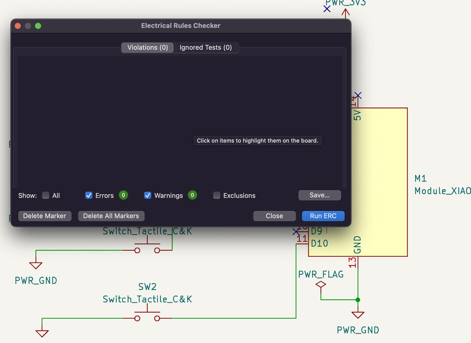
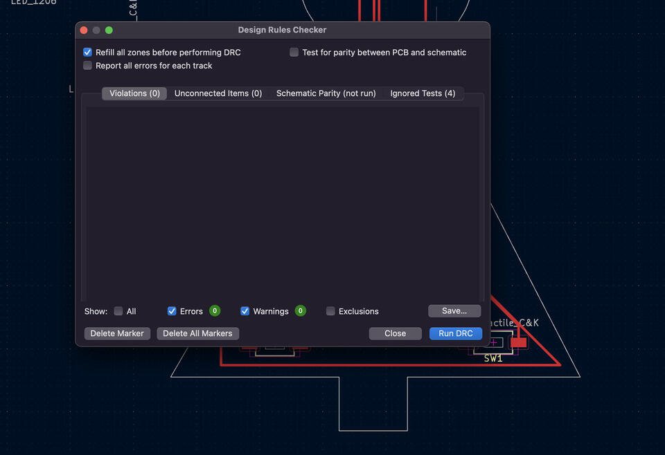
Step 5: Run rules check. Fix any errors.
Step 6: We can now open PCB in board editor.
To note some potentially useful information about this stage:
- label things for clearer design - modularize the schema, especially useful for more complicated designs
- let’s use the 0.05in grid for laying out the components
- it is important to read the datasheets of the components we are using, for example, to find out the voltage they require or what is the max/min current they can take without being damaged/performing poorly. When you select the component and press “CONTROL+D”, it will open the datasheet for you. We can also check the electronic inventory, e.g. the part we are supposed to have in the lab (http://inventory.fabcloud.io/?purpose=Electronics%20Design), or one can also check the DigiKey.
- this is the stage where we should calculate what kind of components we need - for example what is an appropriate resistor with our LED, so it won’t burn, but will still shine bright (there should be recommended current in the data sheet). In KiCAD we can calculate it using text, but also can do it on the side -> with R = V/I (V = IR)
- “right click + edit main fields + edit value” can then change the name of the component (led1, main switch etc.)
KiCAD PCB Editor
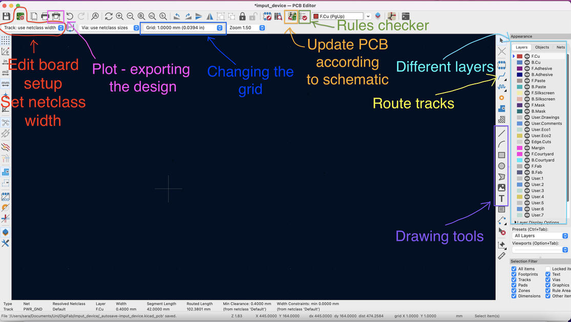
I once again tried to note the most crucial functions of the PCB board editor. Here the grid is quite important as it will determine how far the components are in the final cut board.
Step 1: Hit update PCB with will transfer all the changes made to the schematic.
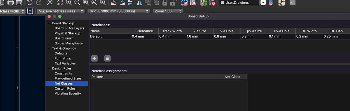
Step 2: Edit board setup and change the netclass to be compliant with the machine we have. 0.4 millimeters is the smallest we can mill, so we should change the 0.2 no 0.4, and them also the track width to 0.4 mm (and the rest as per Figure 10).
Step 3: Make sure the grid is what we want. In general, it is good if we are laying components to the 0.1 mm grid.
Step 4: Organize your component the way you want them to be on your carved PCB board.
Step 5: It is important to recognize what should be at which layer. The wiring should be at Cu layer, the outline of the board at the Edge layer (as this will be cut through the whole board) and so on.
Step 6: Add the wiring and draw the outline. I find it helpful to do the whole wiring by myself, but you can also hit “CONTROL + F” at any point in the journey, and the KiCAD will automatically connect the selected pin to its destination.
Step 7: Run rules check. Fix any errors.
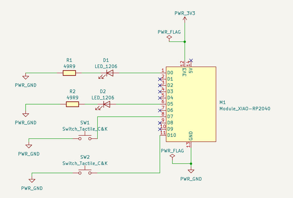
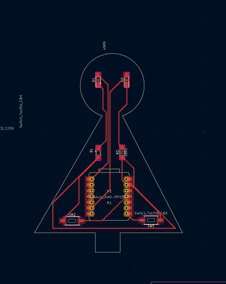
I wanted to design a simple shield for an XIAO board - containing two LEDs and two buttons. This is my final design:
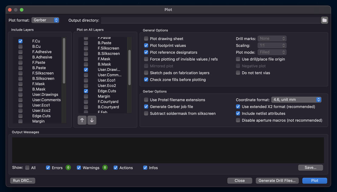
Now the design is ready, we can export it as a Gerber file (using a plot function), so we can mill it. The Figure 13 shows settings I used. I like to have all my layers in a single file, and then play with it a bit more in the VCarve program. We can first generate the drill file, and then plot (although I usually don’t use the drill file but add the holes “manually”).
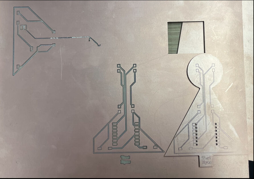
Milled board
During the electronic production week, I have milled the board (though rather unsuccessfully as back then the PCB milling machine was poorly leveled).
Files
Download KiCAD files used in this week - [Zip file]