Week 8: Electronic Production
Group Assignments:
Characterize the design rules for your in-house PCB production process: document feeds, speeds, plunge rate, depth of cut (traces and outline) and tooling.
Document your work to the group work page and reflect on your individual page what you learned.
For the group assignment we had to make line test traces for the traces and the outline. This test will show the traces thickness with different sizes ranging from 0.001inch up to 0.02inch.
To do this, following the same procedure for preparing the machine and mods settings for both, traces and the outline, the calculating tool path was as shown below:

Following the previous steps for cutting, for traces and outline the result was as shown below:
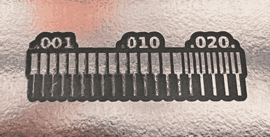
From the result, I think thickness on 0.016inch which almost 0.4mm is enough in general, but if we have a components that needs high current, maybe we could make the traces thicker.
Individual Assignments:
In this week I need to produce my PCB board that I design it at week 6 using the cnc roland machine but in this week I will not use a smd potentiometer as I did in week 6 rather than that I will use a potentiometer with legs which will be connected by through hole ,so my circuit contain a MCU,red led and potentiometer so to connect those component I need to use through hole and smd connection , so I need to use both side of my pcb board to connect the leg of the potentiometer ,
so in Eagle software , I used layer visibility in Eagle to extract the view picture I need , one for the top layer ,one for the bottom and the last one for the cut outline and hole drill ,
Process for that is follow the following steps :
Pressing the layer icon to show all layer in the drawing
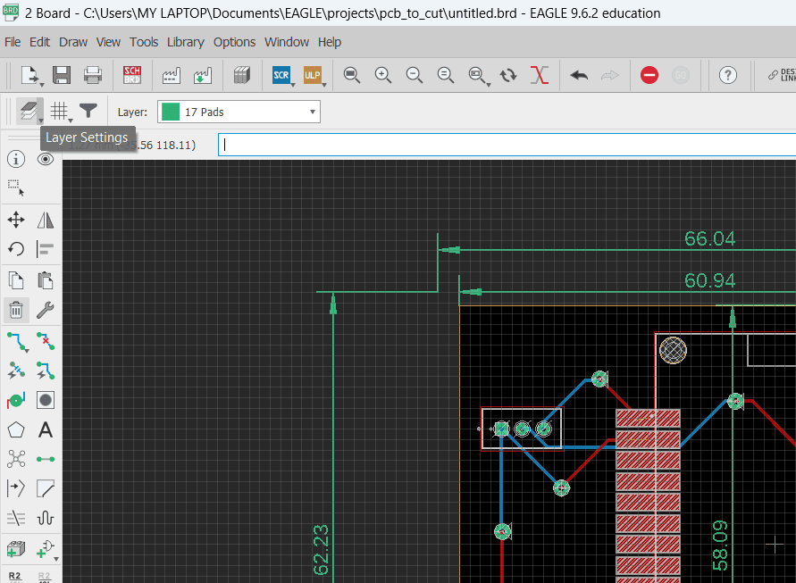
from filter chose used layer
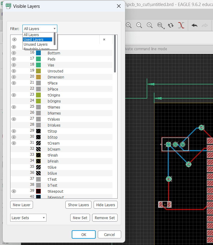
Hide all layer
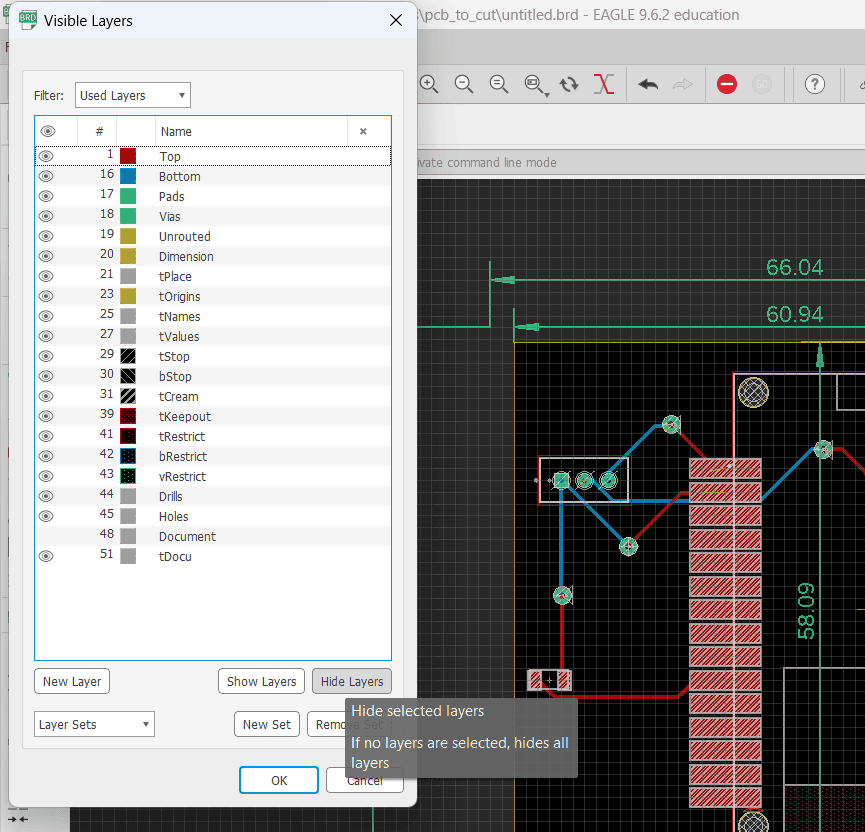
show layer view that you need
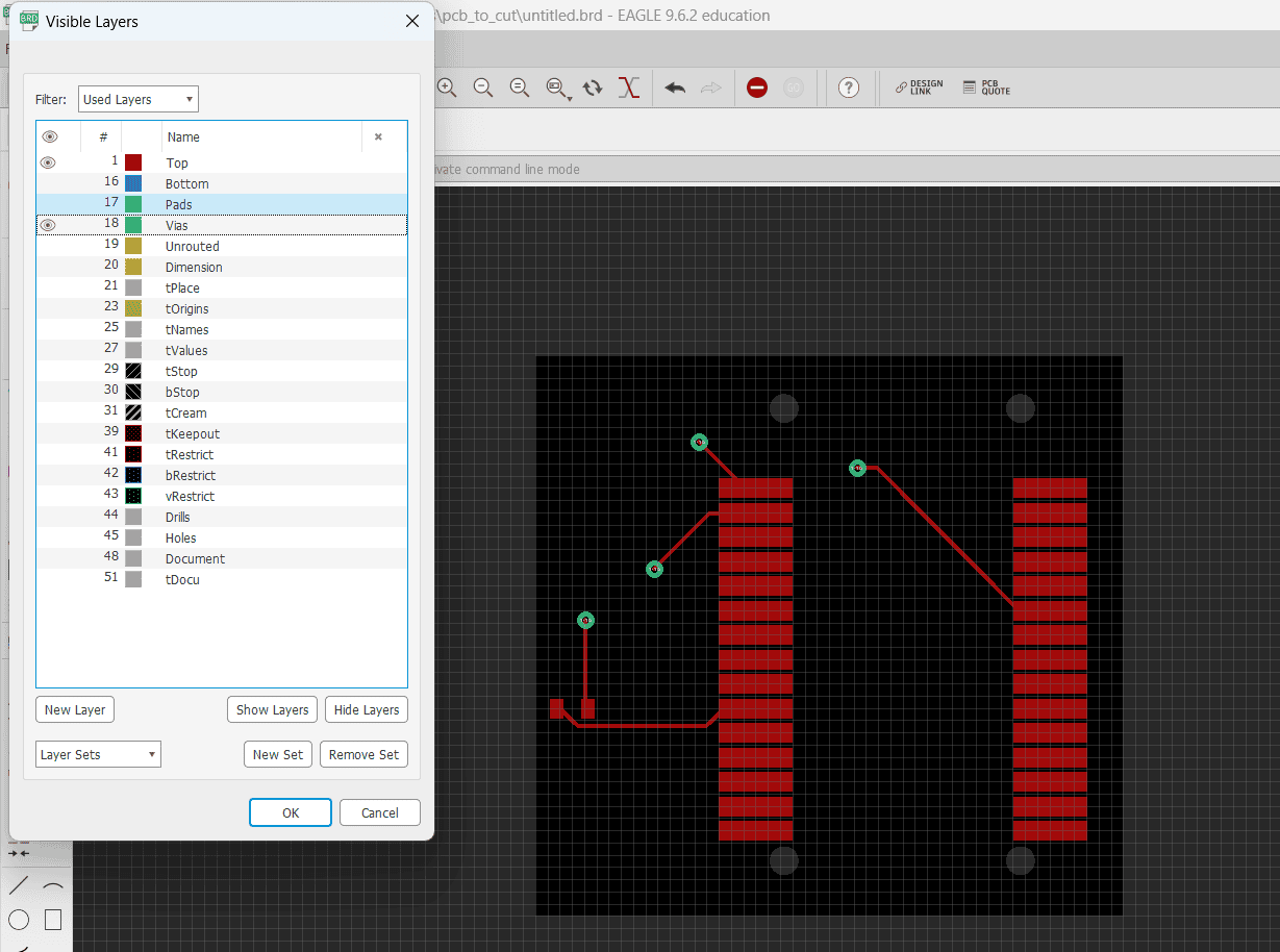
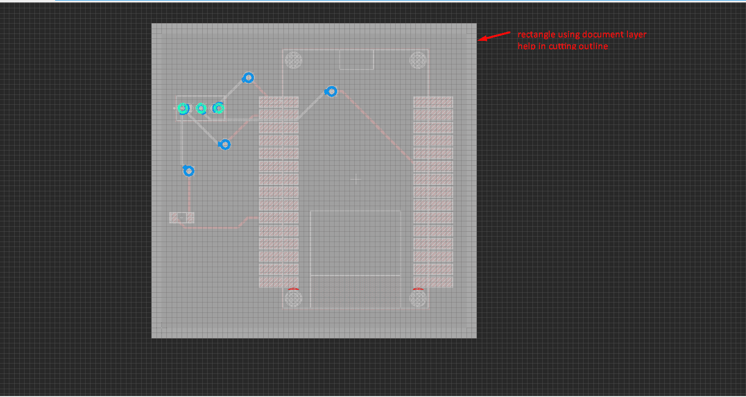
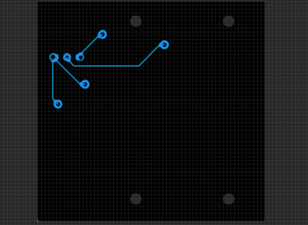
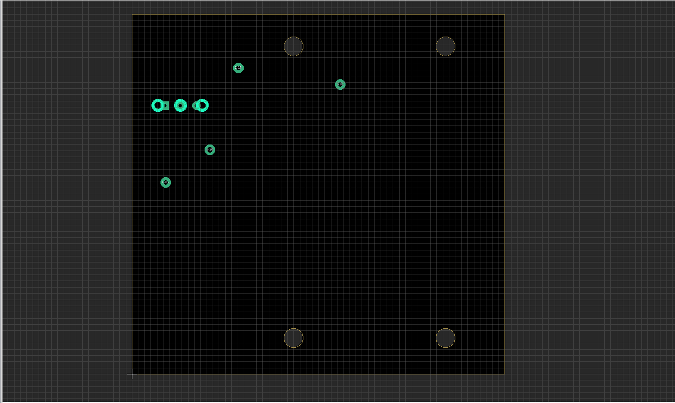
I have three view one for top layer and one for bottom layer and one for cut outline and holes ,before taking views, I will draw a rectangle around the pcb board that will help in the cut outline of the board as below using layer document
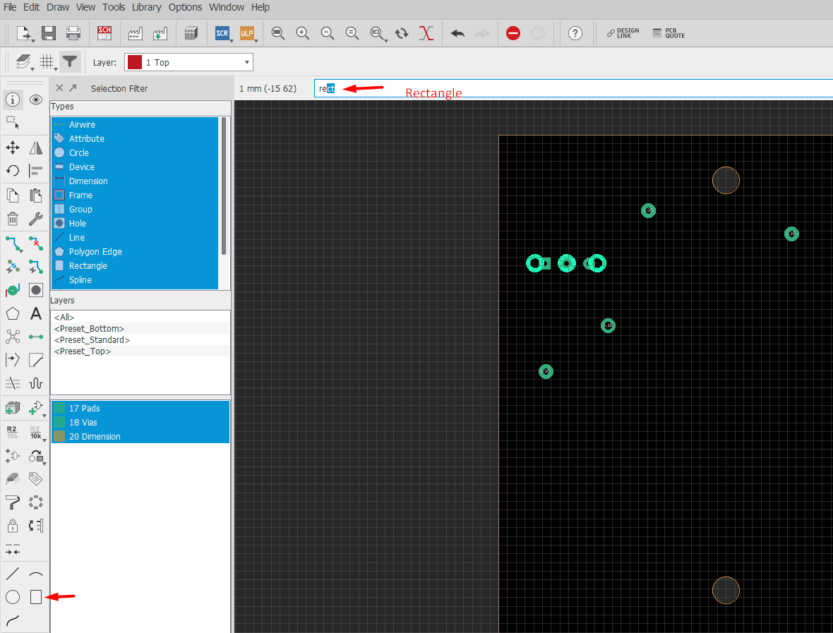
Top layer view
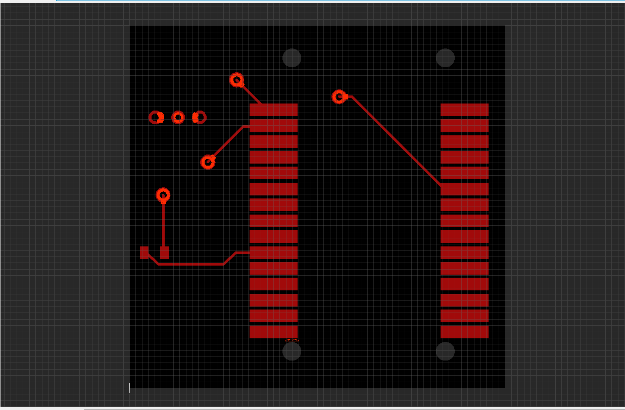
bottom layer view
cut outline and holes view
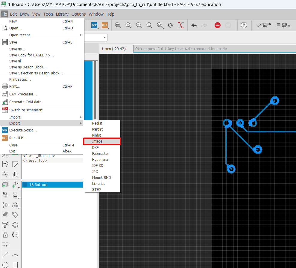
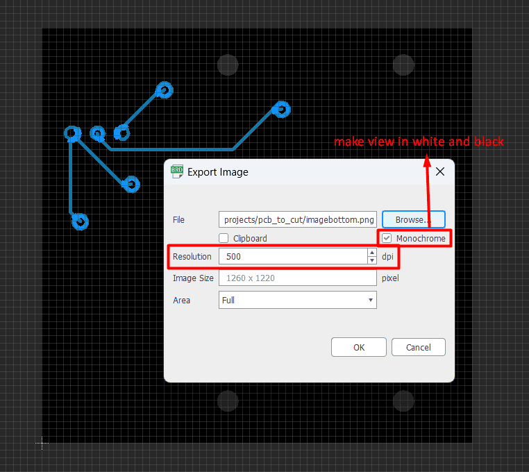
I need to export those images as png and in white and black ,since modes(online web help to generate cam file for pcb cnc ) see picture in white and black (it remove black color and keep white color)
export view as png
I take a 1000 dpi resolution , you can chose more for more detailed view,but note you should chose the same resolution for all your views to prevent any scale issue
view of bottom trace

view of top trace
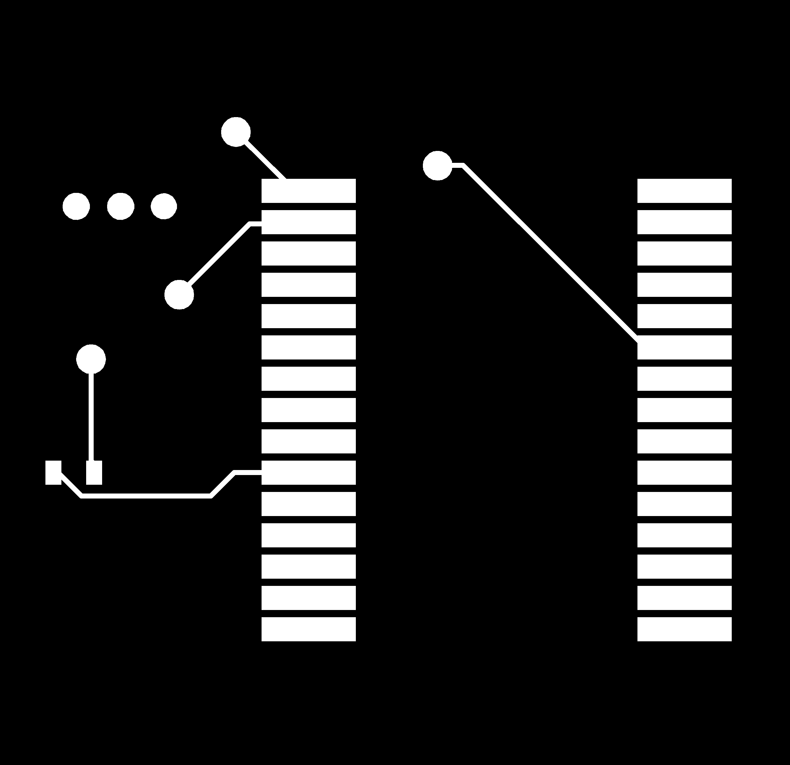
view of the outline of PCB ,but I need to modify on the color of the image using paint software as below
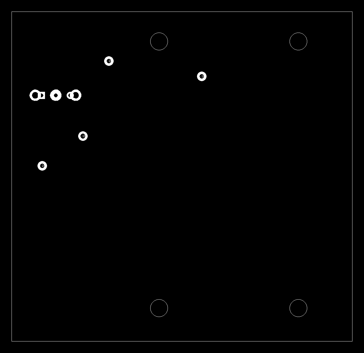
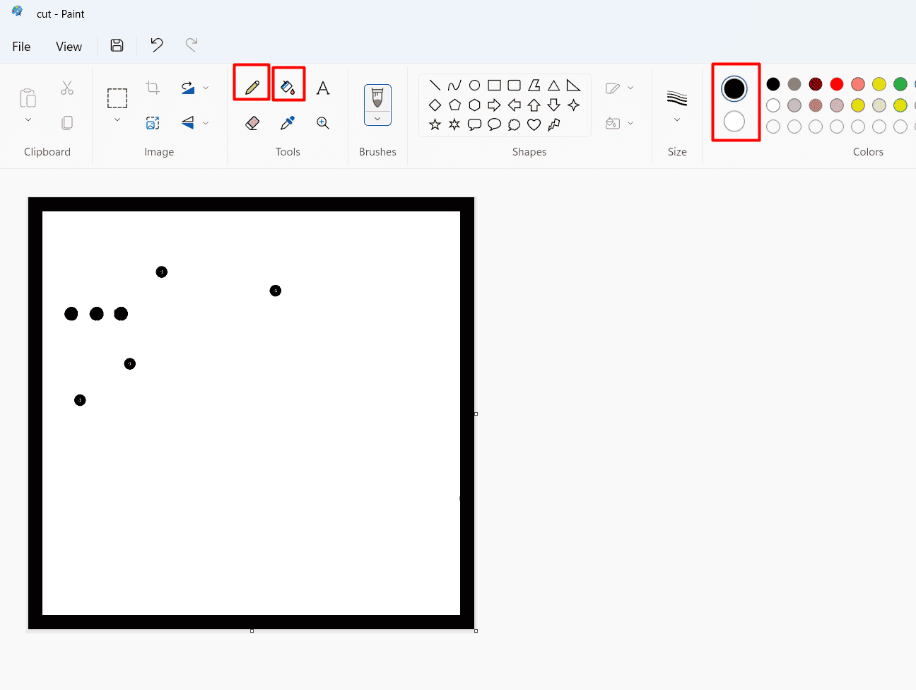
cut outline view after modification
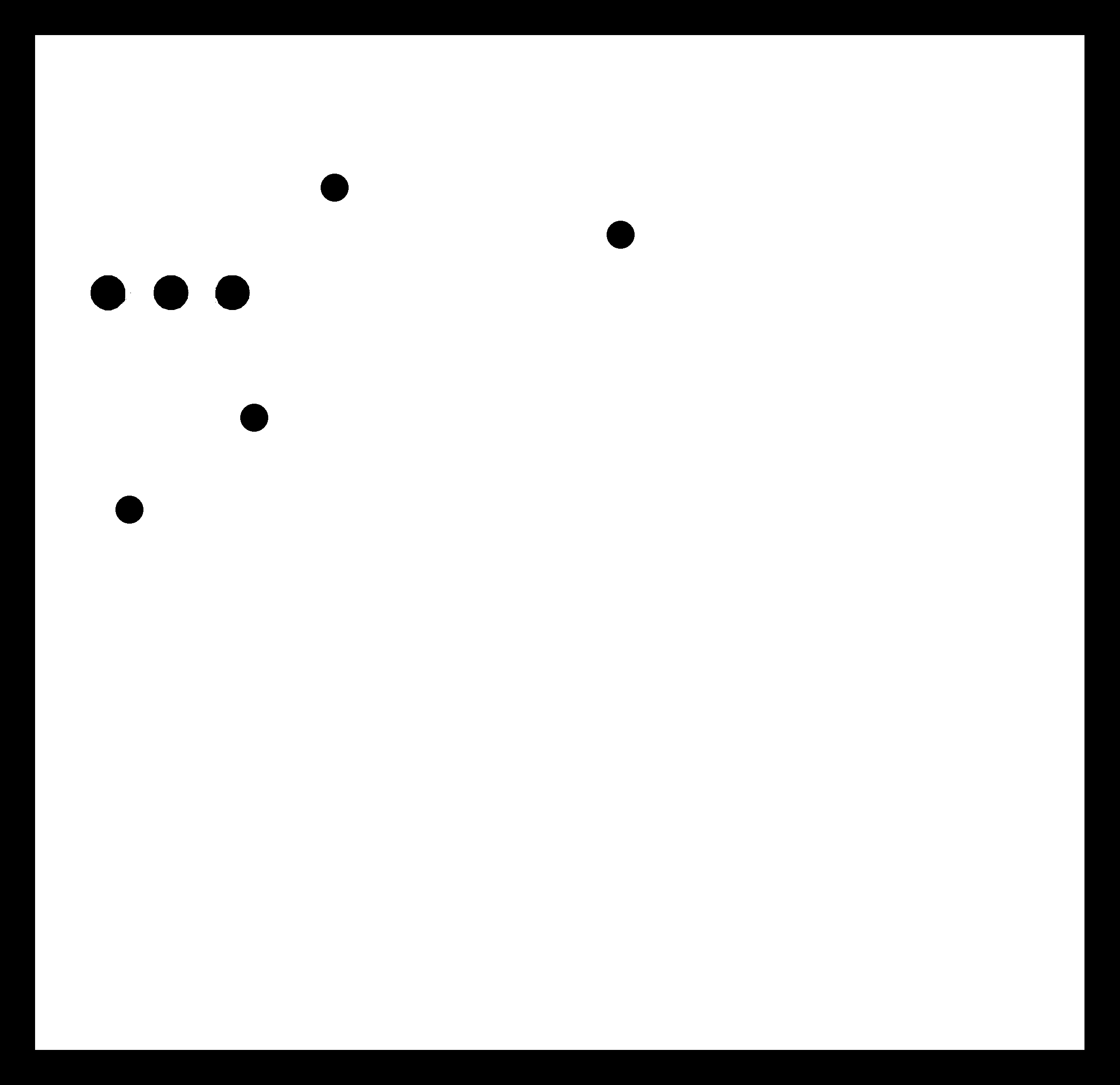
While preparing the board view, I faced a problem where the hole diameter for the potentiometer footprint was smaller than the diameter of the potentiometer that I had. Additionally, I wanted to add a circular ring around the hole to make wiring and soldering easier.
My first attempt to modify this was by exporting the board view to DXF and opening it in AutoCAD to draw the necessary parts. Unfortunately, I discovered that AutoCAD rescaled the board size and changed its value. As a result, when I cut the board, I encountered problems.
After realizing this, I switched to using Eagle and discovered that I could add circles and other shapes using this software. This allowed me to modify the design and solve the problem I was facing with the hole size and the need for a circular ring.
now I will use modsproject website to generate the G-code for the design
by clicking mouse right click then chose program then chose open program
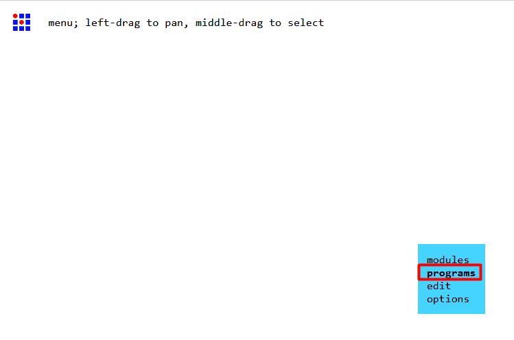
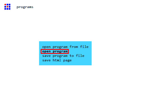
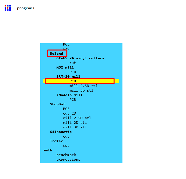
here you chose the machine that you will use for me I will use Roland machine SRM-20
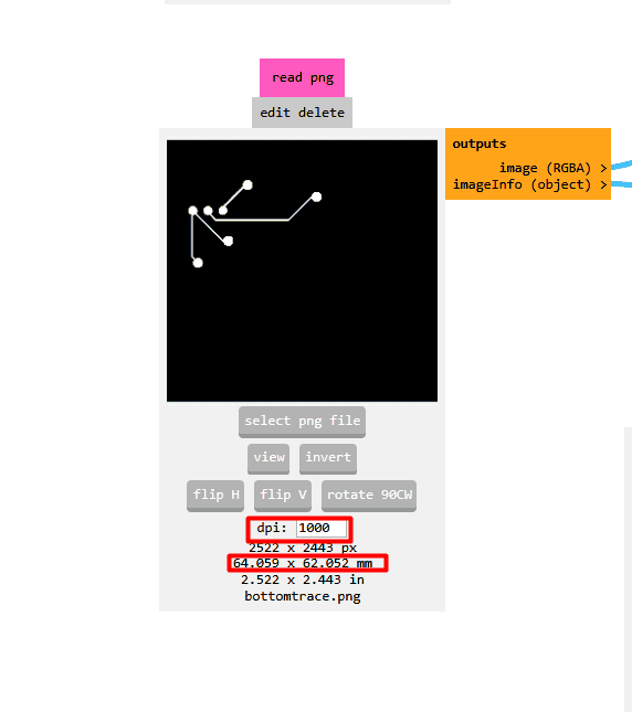
now ,you will add the image that you make by click on select png file ,an important note that you will need to check that the dpi are the same as you save the image with ,since if it change that will affect the size of image and its components
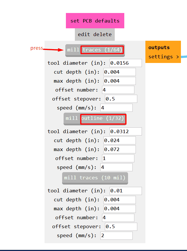
now you will chose the tool for the task,there is two task one for the trace that we will use 1/64 inch tool and for cutting the outline of the board we will use 1/32 inch tool which is larger
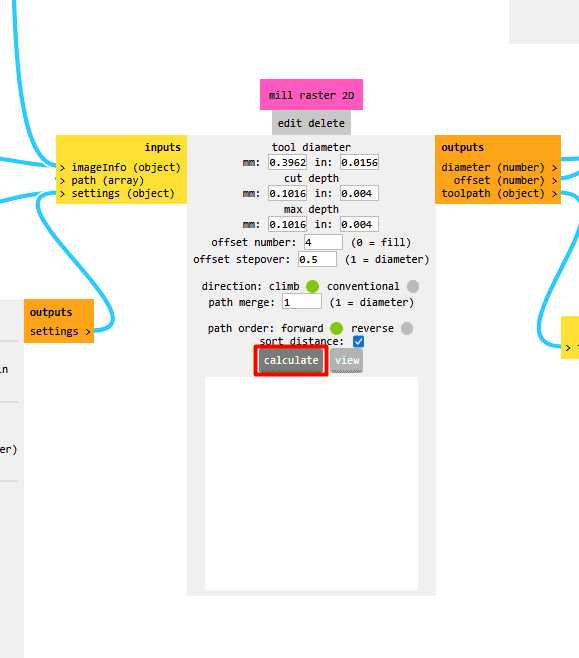
now we will click on calculate button to see the preview of the tool path , by click on view you will see and check how the tool will move
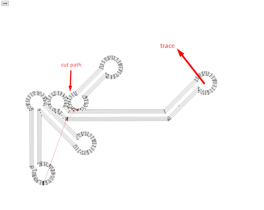
the black arrow represent the tool movement
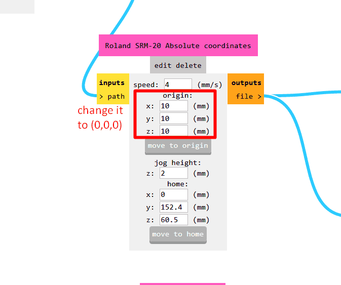
important step to set the absolute origin for the machine to be (0,0,0)
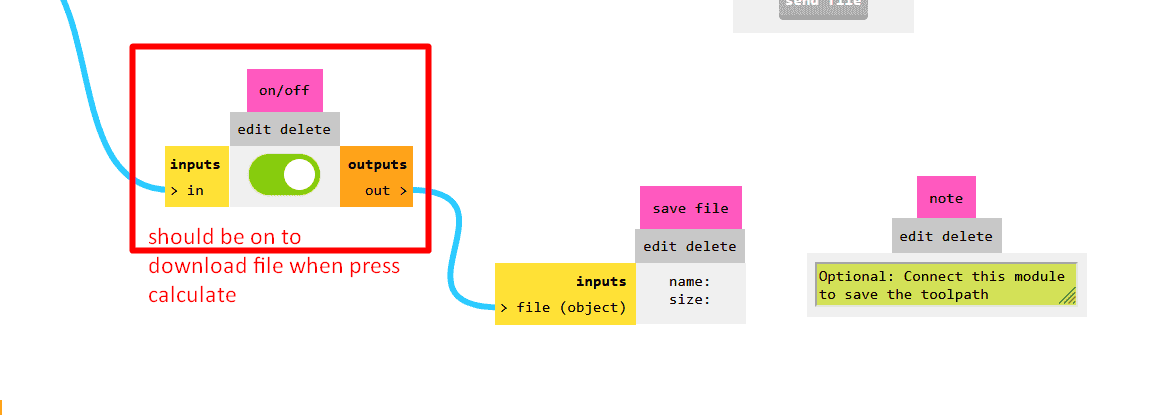
To download the G-code file you need to activate this module , by that the file will be download when you click on calculate button
now we will go to the machine and its interface software
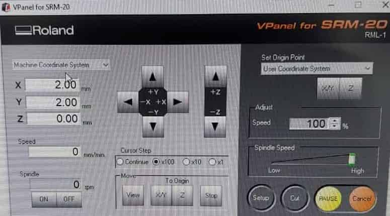
our Roland machine srm-20 it has its own software which called vpanel for srm20
.jpg)
for roland software interface there are two coordinate the machine coordinate and the user coordinate ,user coordinate can be changed to use it for the production process ,
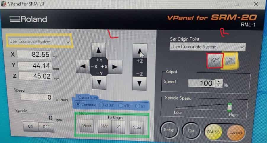
there are two main part ,the left part and right part , in the left part you can move the machine tool by the arrows in x and y plane horizontally and in z coordinate vertically ,the movement steps value can be determine with blue highlighted part,also you can move the tool for its origin in x and y also for its z zero value by clicking on the buttons in the green highlighted part ,for the right side you will determine the new value for the new origin that you will use for both the x and y value and also for the z value
set z zero value
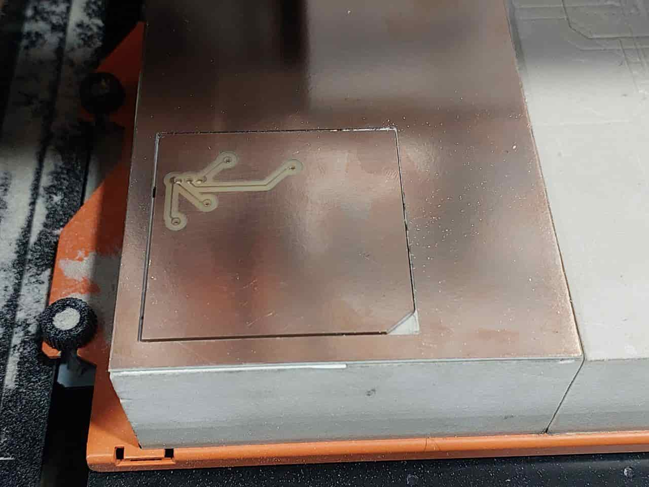
To begin with, I placed the copper piece onto the board and secured it using double face tape. Then, I initiated the first program, which traced the top layer, followed by cutting the outline of the piece. Afterward, I flipped the piece and created a chamfer on one of its edges to ensure proper alignment with board edges. It is important to note that for the bottom side, I undertook two crucial steps. Firstly, I horizontally flipped the image while generating its G-code path on modsproject website. Secondly, I shifted the origin by the tool diameter in both x and y directions, by moving origin value forward by (tool diameter ) in x and y
in vpanel for srm20 software add file to cut

bottom side
top side
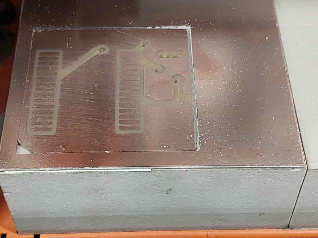
I encountered a problem when I forgot to relocate the X-Y axis after flipping the board. Specifically, I forgot to remove the tool diameter value from its original X-Y position and create a new origin. As a result, you can see that the holes are slightly shifted from their original locations. However, this does not impact the circuit's functionality.
then I start the soldering part
potentiometer through hole
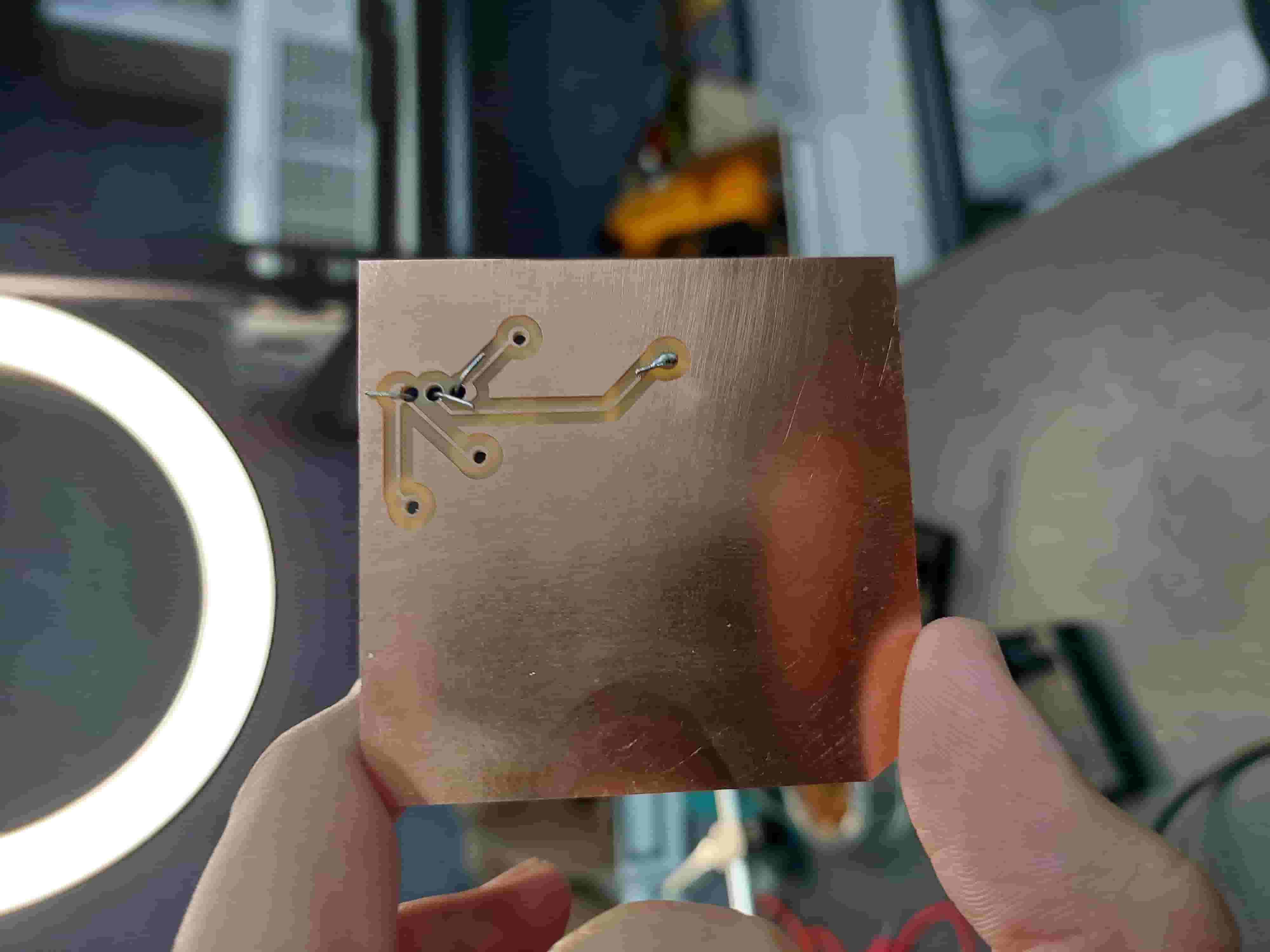
I solder the potentiometer from the bottom after bending its leg
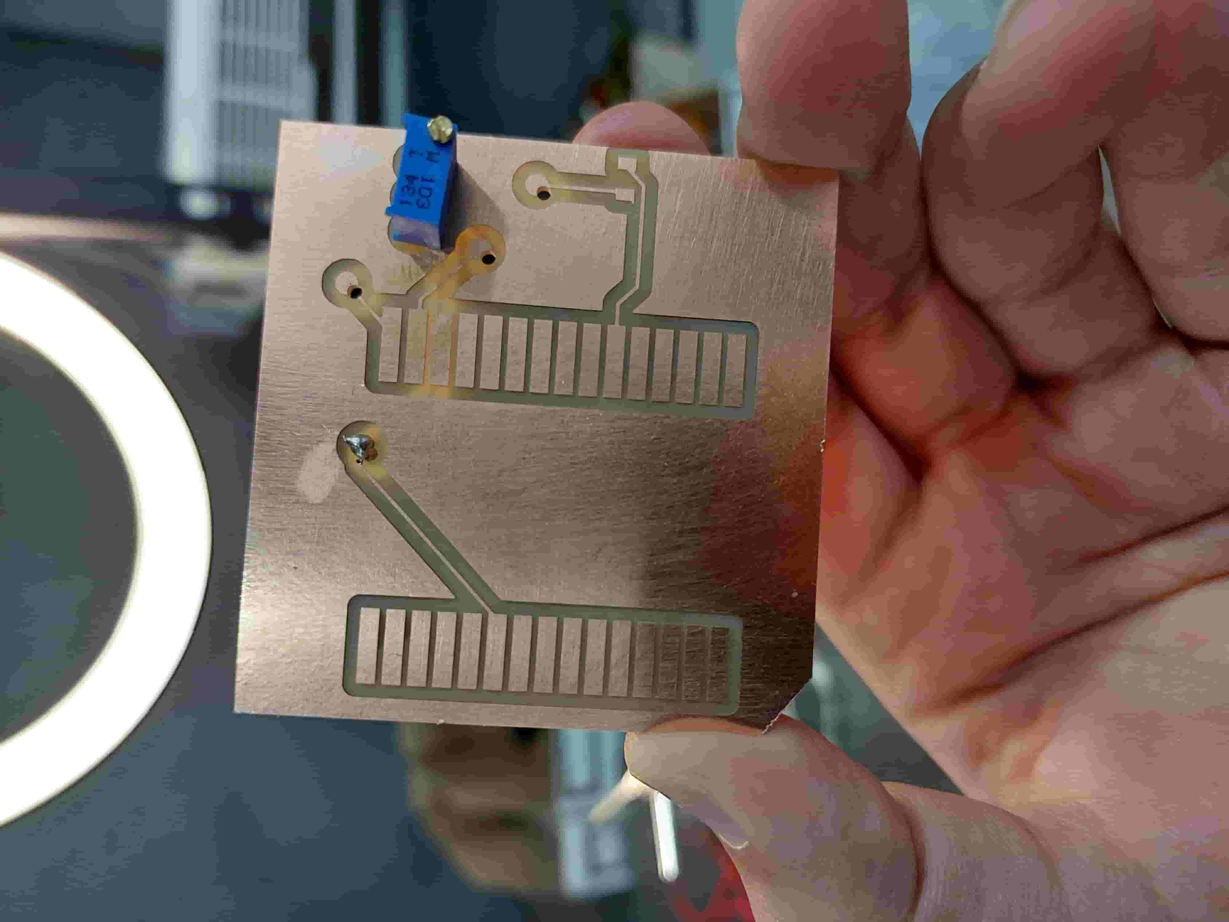
To connect the top and bottom sides, I first removed the insulation from the jumper wire. Once the wire was exposed, I used it to establish the necessary connection between the two sides.
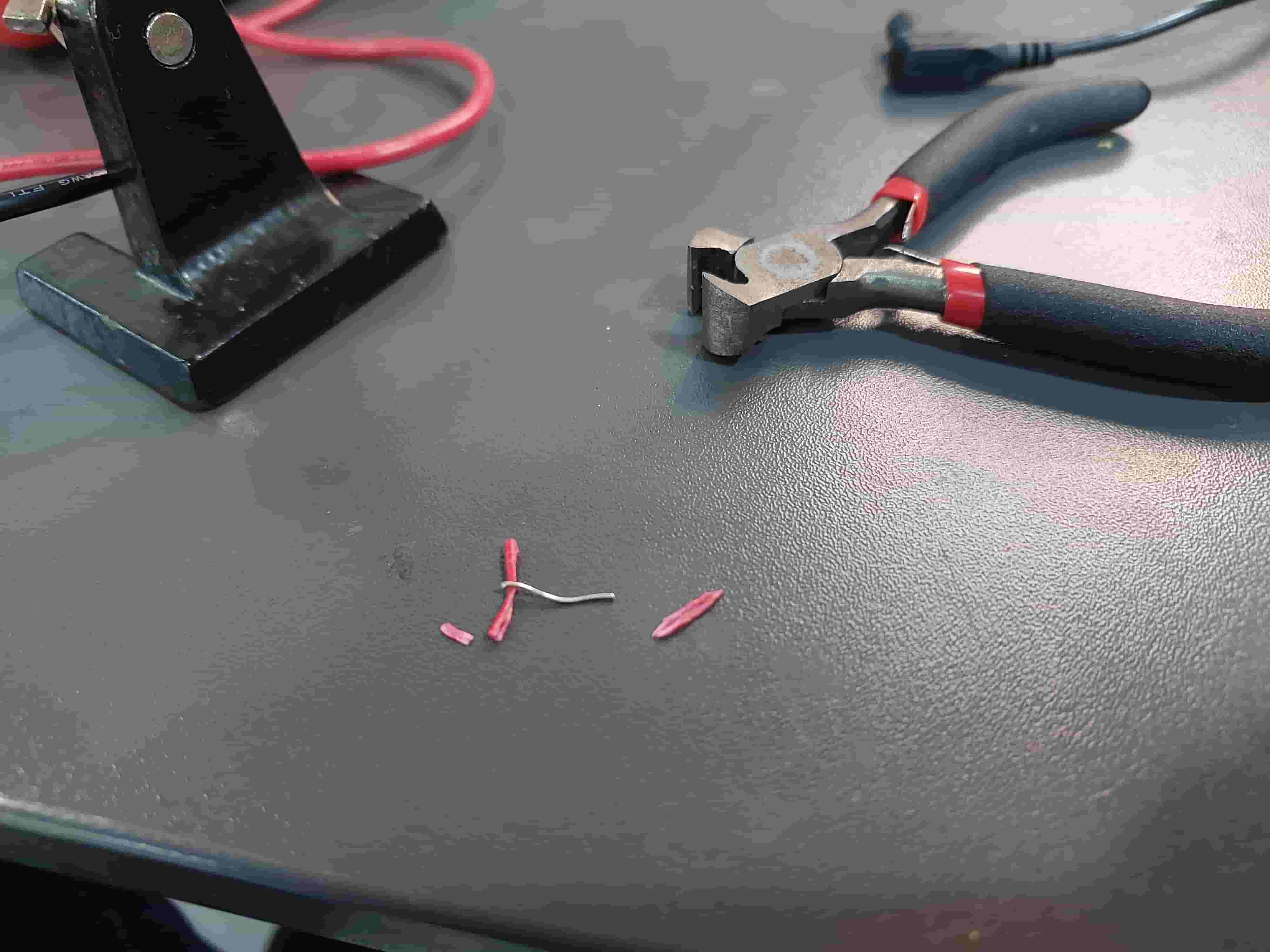
I passed the jumper wire through all the necessary holes. Once I had the wire in place, I proceeded to solder the required points. Finally, I cut off any excess wire that was left after the soldering was complete.
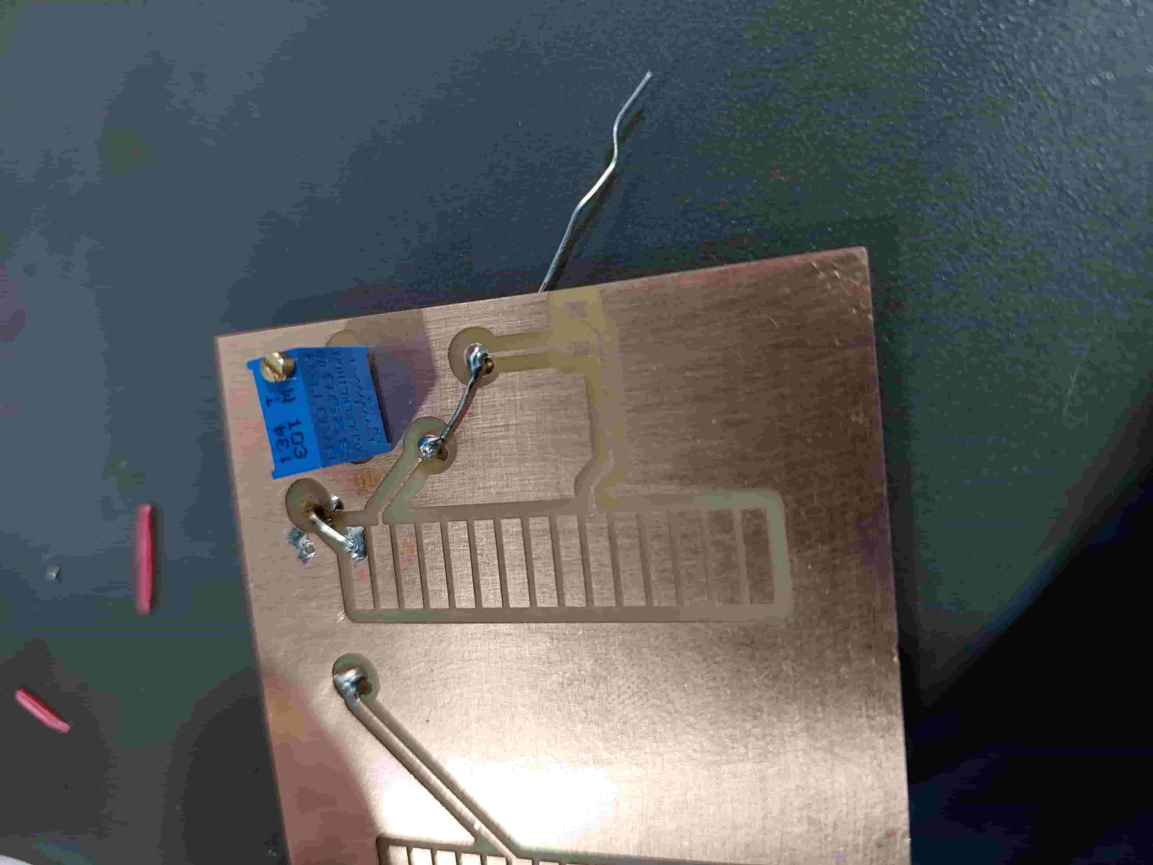
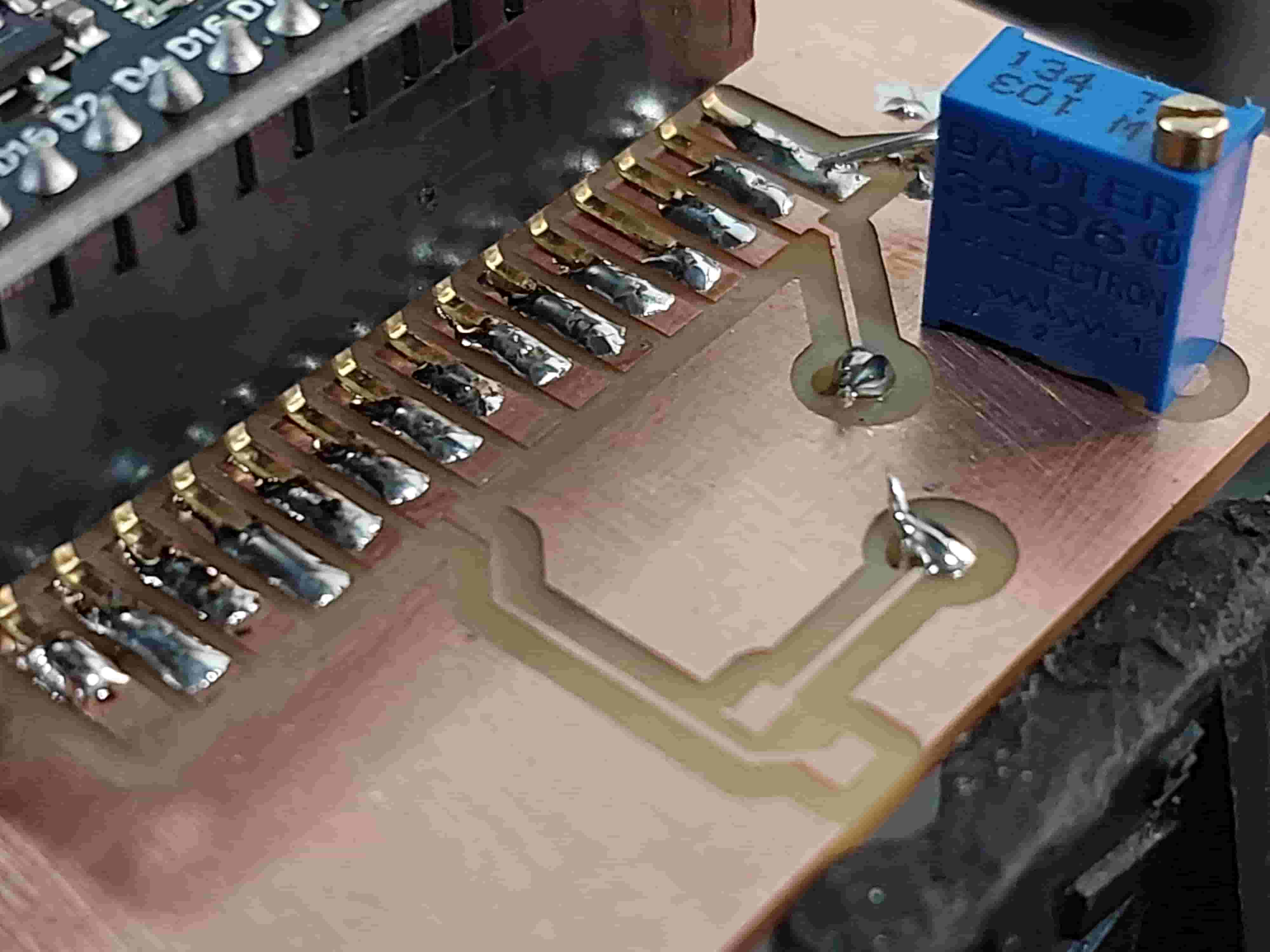
I soldered the legs of the ESP32 to their designated places. Then, I proceeded to solder the red LED component to its respective position.
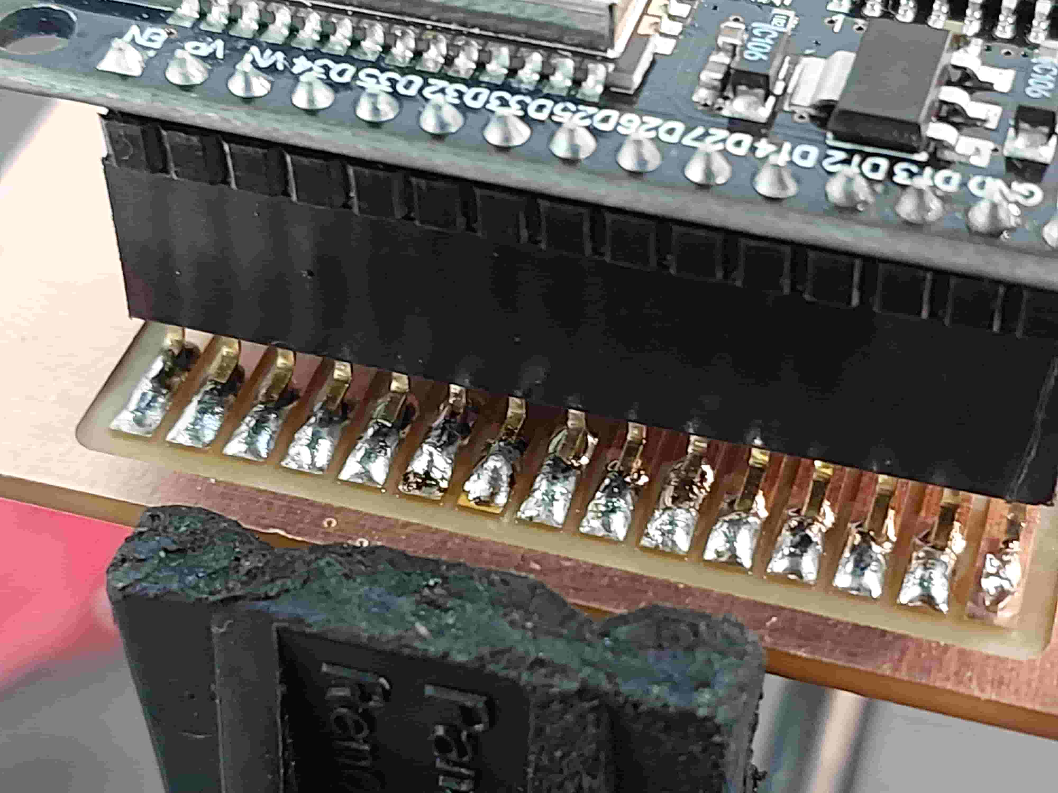
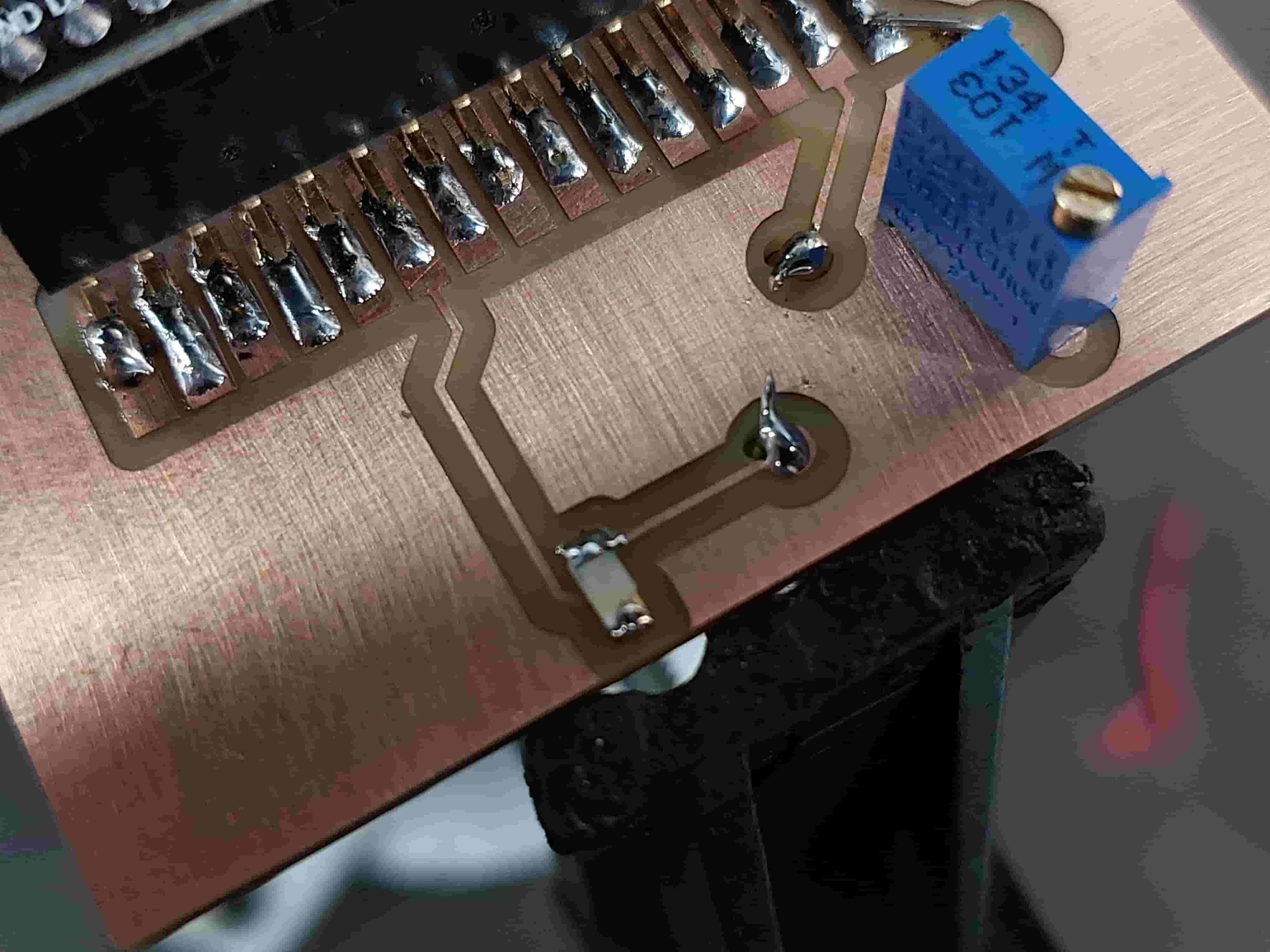
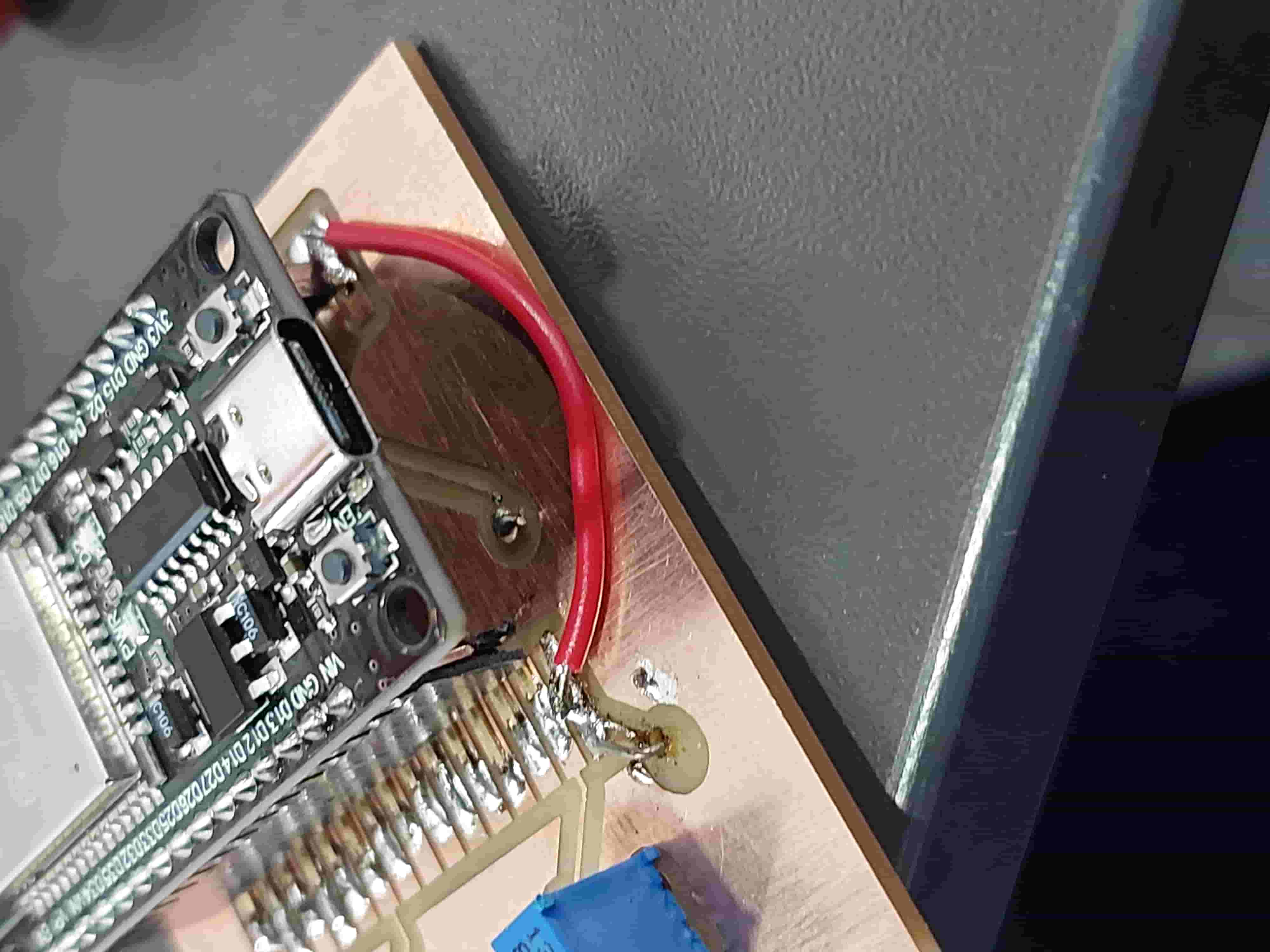
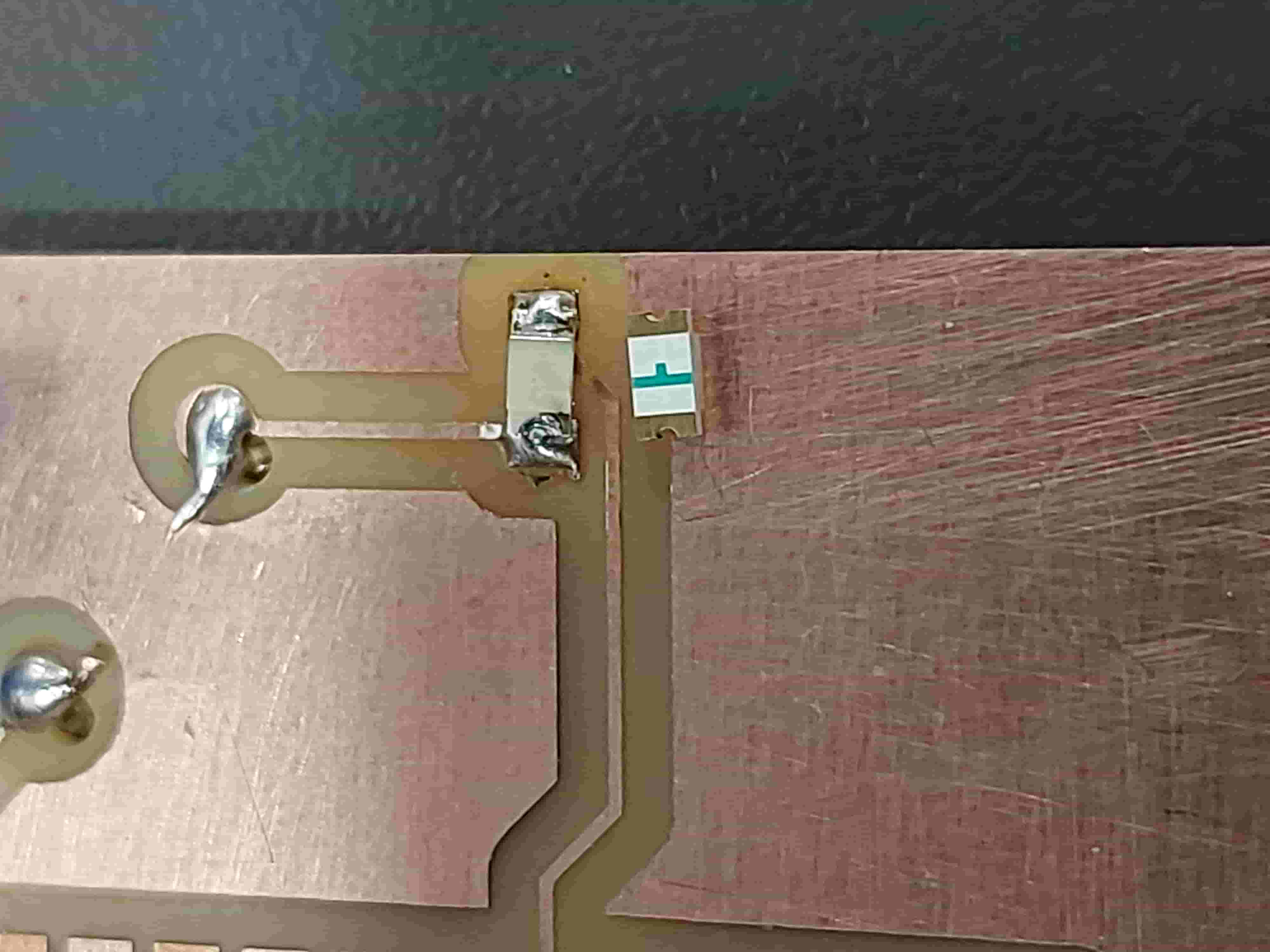
After soldering the components, I realized that I had mistakenly used the VIN pin instead of the 3V pin. To rectify this issue, I used a jumper wire to connect the 3V pin to the corresponding point. Additionally, I also had an issue with the orientation of the red LED. To ensure proper soldering of the LED, I referred to the datasheet for the component to verify the correct orientation. It is important to consult the datasheet for each component before soldering to ensure accurate and proper placement.
the current flow from right to left
I check the connection conductivity using the multimeter , then I upload the code to the microcontroller and having this result
Arduino code
              int pot_value = 27;   // select the input pin for the potentiometer
              int ledPin = 19;      // select the pin for the LED
              int sensorValue = 0;  // variable to store the value coming from the sensor

              void setup() {
                Serial.begin(9600);
                pinMode(ledPin, OUTPUT); // declare the ledPin as an OUTPUT
                pinMode(pot_value, INPUT); //declare the pot_value as an INPUT
              }

              void loop() {
              // read the value from the potentiometer:
              sensorValue = analogRead(pot_value);

                //led blinking
                //turn led on
                digitalWrite(ledPin, HIGH);
                // stop the program for  milliseconds:
                delay(sensorValue);
                //turn led off
                digitalWrite(ledPin, LOW);
                // stop the program for  milliseconds:
                delay(sensorValue);
               }
Code Explanation
Code Overview
The code controls an LED's blinking pattern using a potentiometer. The LED turns on, pauses for a duration based on the potentiometer's analog value, turns off, and pauses again for the same duration before repeating.
Variables
pot_value: The pin number (27) for the potentiometer input.ledPin: The pin number (19) for the LED output.sensorValue: Stores the analog value from the potentiometer.
Setup Function
- Initializes serial communication and defines pin modes for the LED (output) and potentiometer (input).
Loop Function
- Reads the analog value from the potentiometer into
sensorValue. - Turns on the LED, delays for the duration specified by
sensorValue. - Turns off the LED, delays again for the same duration.
- Loop continues indefinitely, blinking the LED at a speed determined by the potentiometer.
.svg)

