Electronics Design
Another scary one. Oh well.
I tried my hand at KiCAD, SVG-PCB as well as Eagle. After some hiccups and late-starts, I have decided to stick with Eagle, although SVG-PCB's workflow is also tempting at times. I also tried manual vector drawings in CorelDraw - in case desperate times called for desperate measures.
Initial Trials / Day 1
Eagle in Fusion
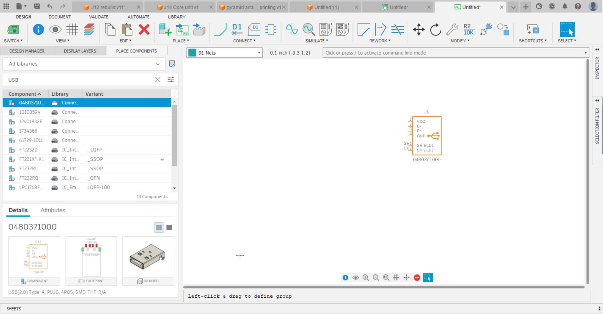
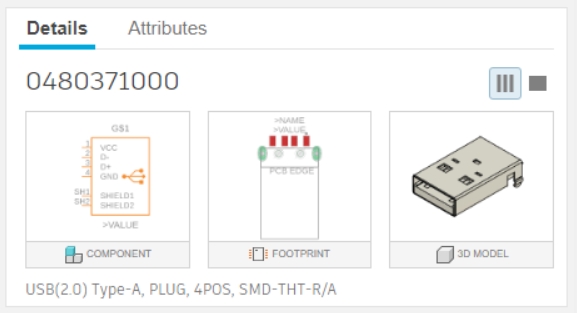
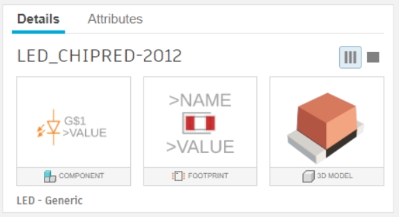
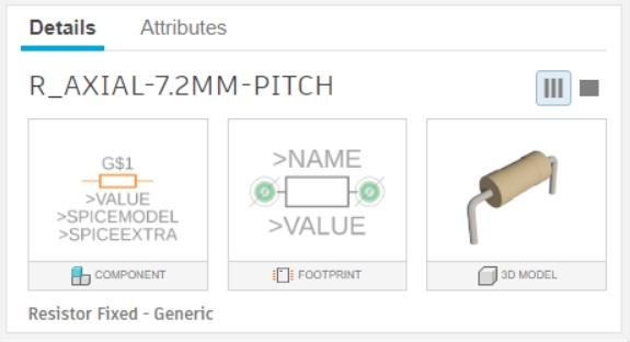
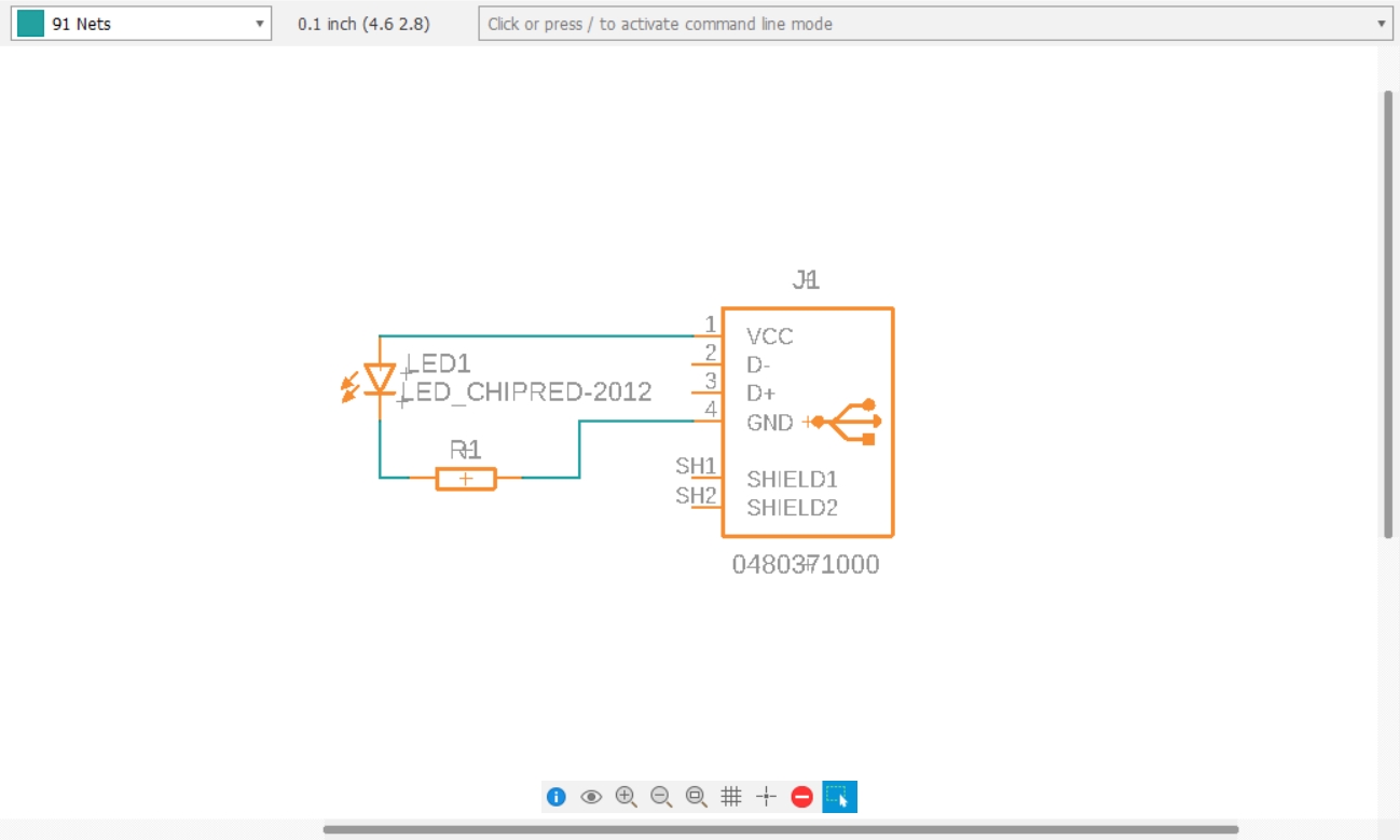
I made a basic USB powered LED circuit, consisting of a USB male, and LED, and a resistor.
Manual vector drawing
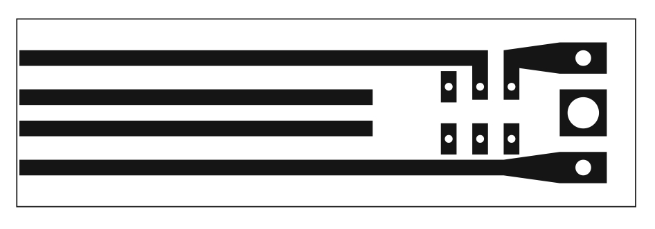
I drew this USB + resistor + LED PCB using a few footprints I found in data sheets. As mentioned above, I would probably take this path only in abject desperation, since the drawing is not parametric and has none of the advantages of being designed on a dedicated KiCAD or Eagle.
However, it's an interesting tangent to create other milled artefacts, not necessarily PCBs, as well as make electronically simple but visually complex PCBs, for whatever ends.
Much Later...
After the above exercise, I was stuck for a long while trying to find the footprints of a particular set of LEDs, trying my hands at KiCAD or figuring if I could draw the footprint in CorelDraw and import a SVG file into either of the EDAs or SVG PCB.
That led to some floundering and backlog, and feeling like I this wasn't something I could do.
Eventually I gave up on those LEDs, and decided to move on with the DevBoard atleast. I got help from the Regional Group with the general advice being to stick to ONE EDA, and preferably Eagle.
Eagle in Fusion, Round 2
I realised I was quite OK with EAGLE, having done the basic USB circuit earlier.
I worked out the basic workflow and created two PCBs.
Ironically, I first worked out a PCB for my Spirograph machine from Week 10. That was a working circuit that I was familiar with, having already created the breadboard and perfboard versions myself. Since it was a definite object that needed to be done instead of an exploratory exercise, I managed to work through some how-to's as needed and figured out things in general. The PCB for the Spirograph machine is documented on it's own page.
Then I attempted the DevBoard for the Seeed XIAO Series, mainly the RP2040.
I studed Adrian Torres' FabXIAO to understand what the devboard entails. Also, this being quite well into week 12 or more, I also knew by now how I wanted things arranged, exposing the I2C and SPI sets of pins separately, giving multiple points for the 5V, 3V3 and GND pins, etc.
I also realised (later than I should have!) that the XIAO series keeps the major pin locations the same. The 5V, GND, 3V3, SPI, I2C, etc all remain the same for the XIAO RP2040, XIAO SamD21, the ESP32, etc, so this devboard will work for multiple MCUs. This was another realisation I had due to the extended time and other intervening electronics exercises, as well as trying out the rest of the XIAO series, mainly the SamD21 and two kinds of ESP32s.
On the design front, I decided to expose all the pins in a series, and also give extra headers for the SPI, I2C and power and GND pins. Here's the work out of the XIAO Devboard.
I first worked out the schematic.
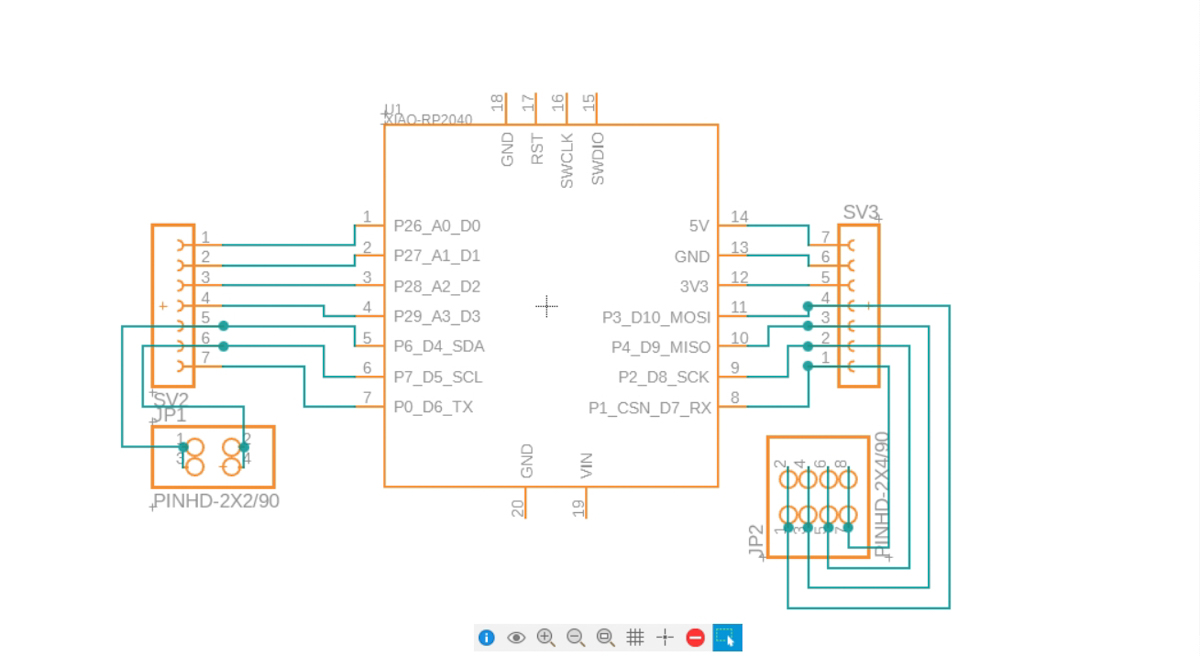
Here's the progress step by step.
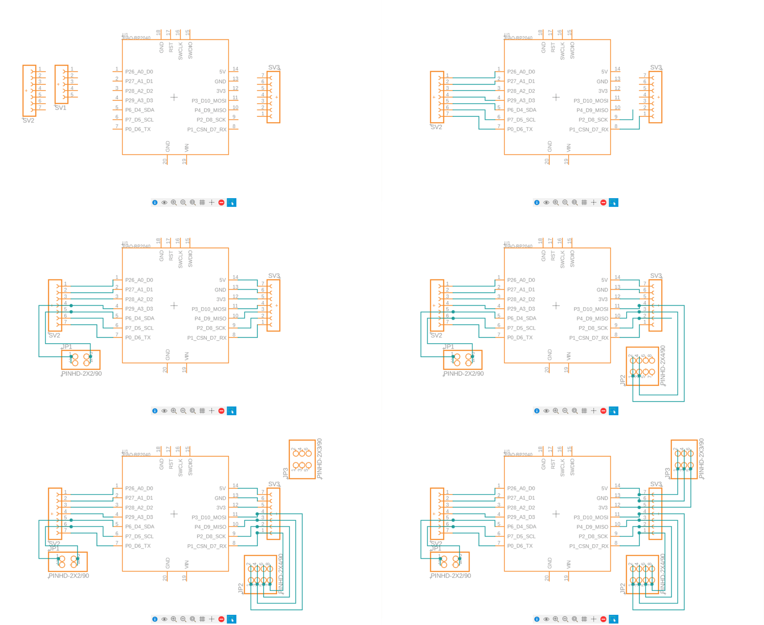
Once the schematic was satisfactory, I moved to the PCB design.
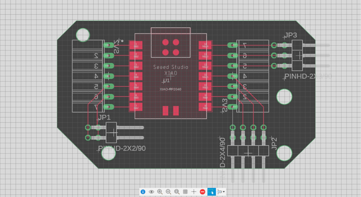
The step-by-step version
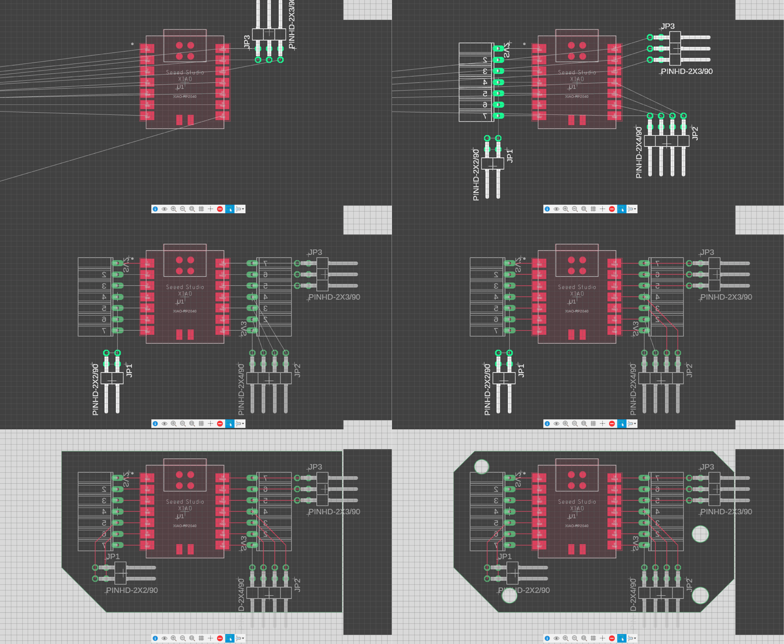
Later, I swapped the 90 degree headers for straight pins.
I also added some mounting holes in empty locations so the board could be screw mounted when needed.
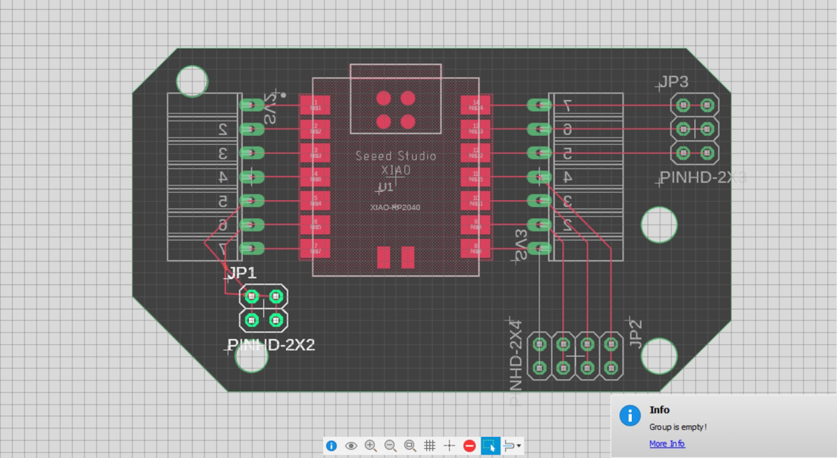
Once done, I checked for errors. Unfortunately, I updated the Design Rules AFTER creating everything, so there were a lot of errors and I had to do a lot of Select-All as well as specific selections to update individual settings. I learnt how important the Selection Filter is here.
I based the rules off the settings I saw on Sibin's page, for KiCAD, and translated as best as I could.
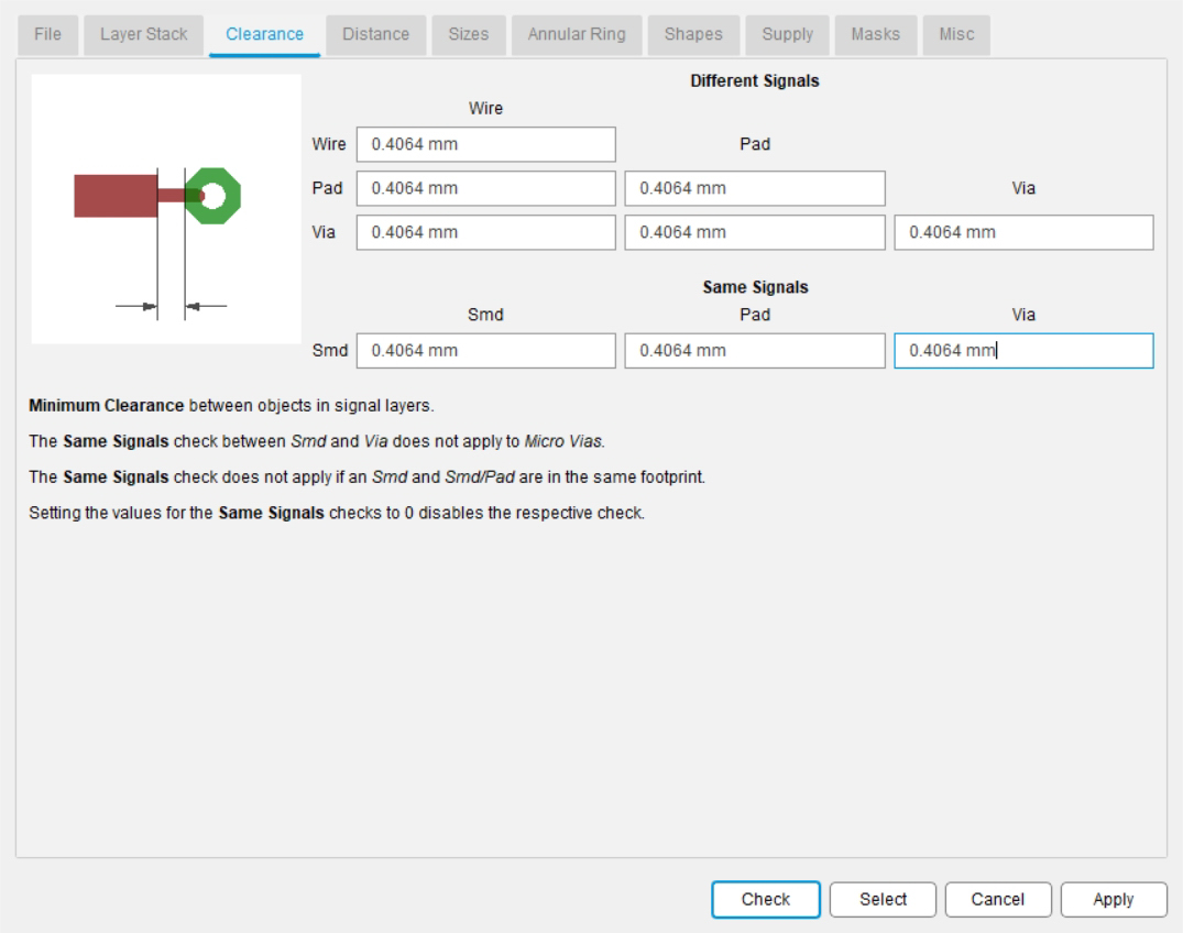
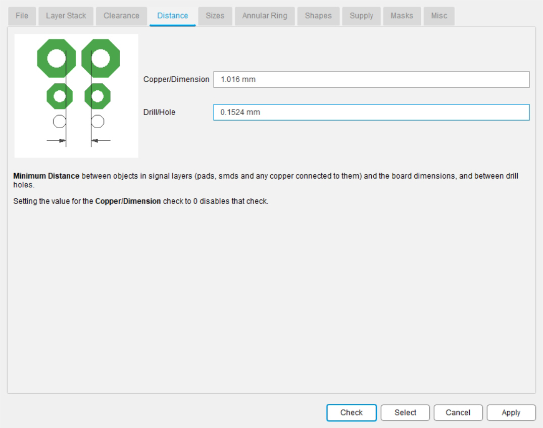
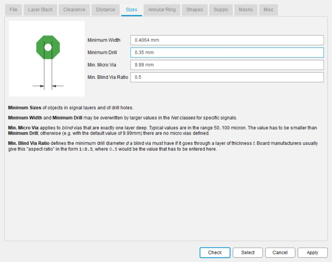
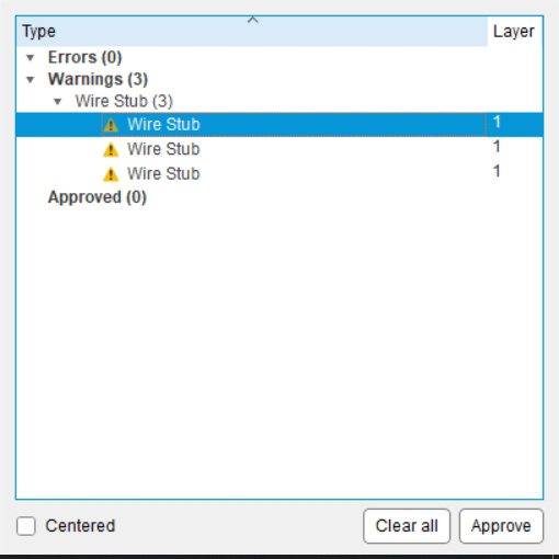
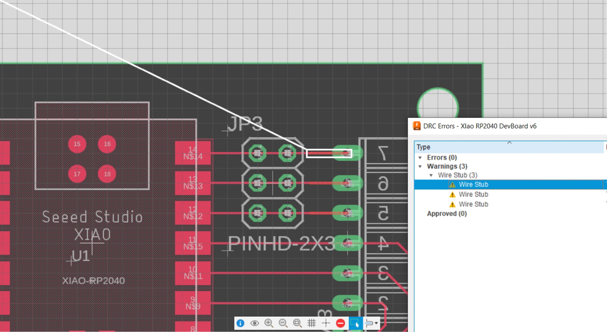
Finally !

This is the evolution of the PCB even after the major design had been done.
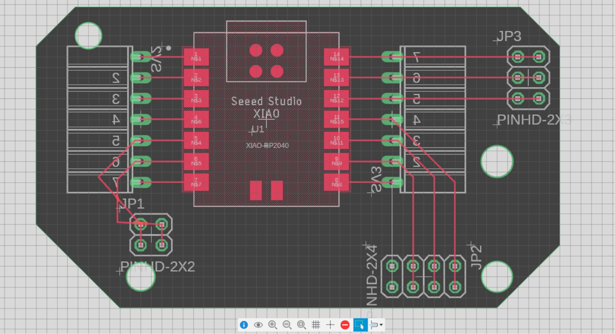
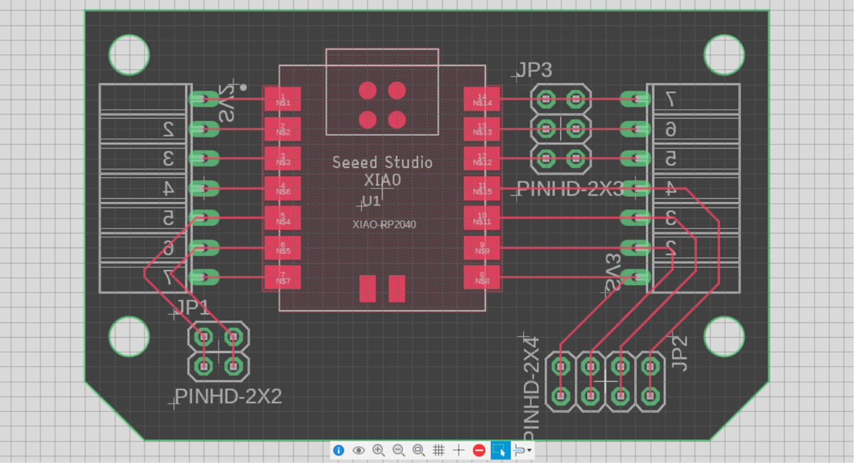 Added better clearances and pathways for the wires, removed bevel corners
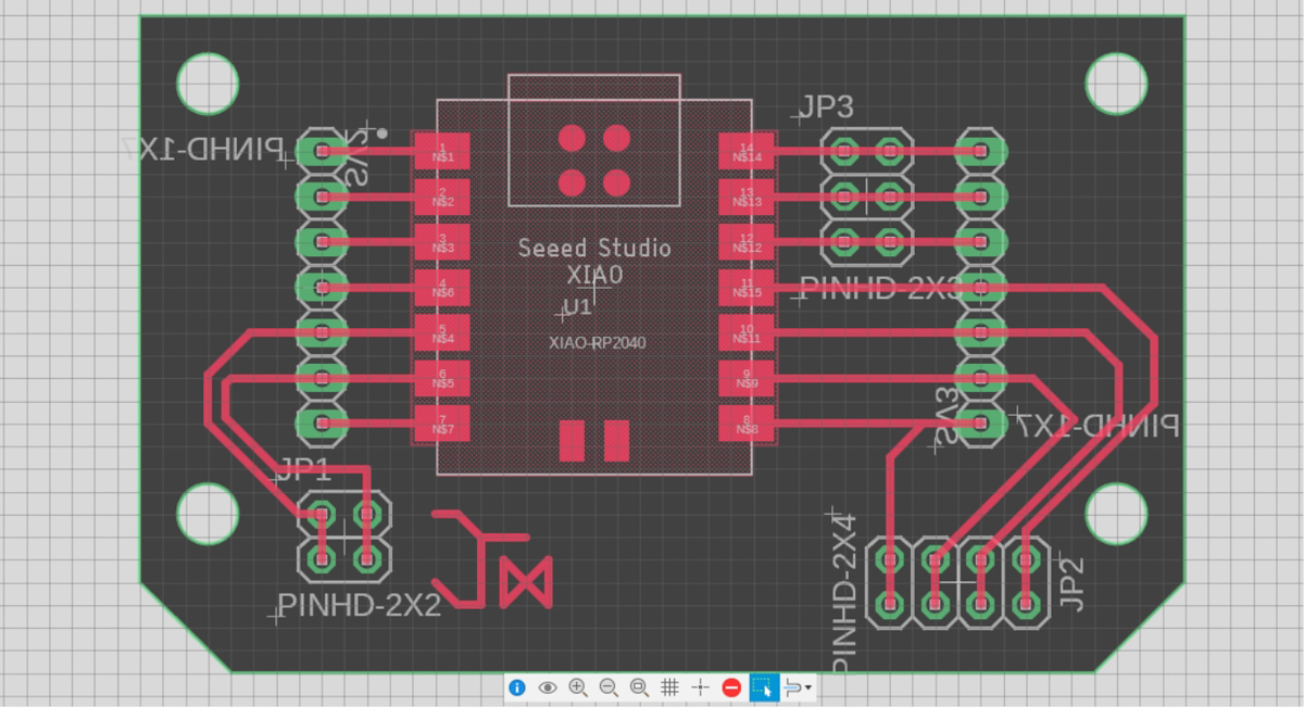 After applying design rules, thicker wires, and changed 90degree headers for straight ones
I also added the my initials JM as wires to personalize the board, inspired by Adrian Torres' graphical 'A'.
This was the version that was milled out for the weekly exercises.
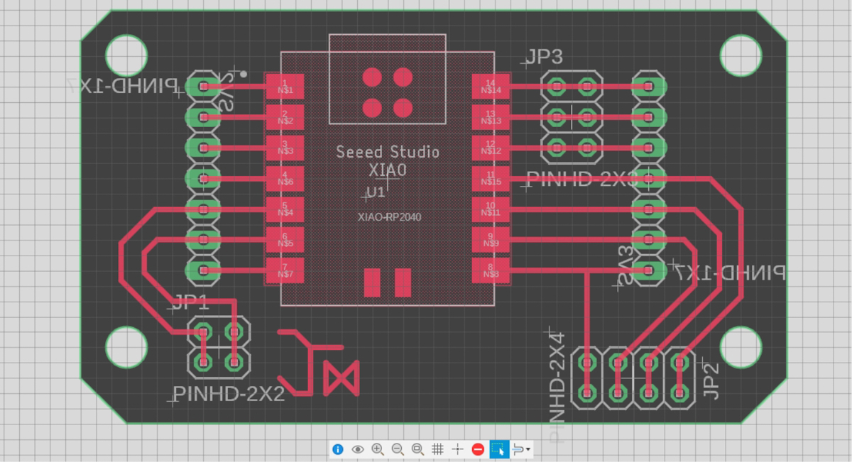 Reworking wire pathways for clarity and ease of soldering, hole positions changed sligtly
This was the version milled out for the final Project.
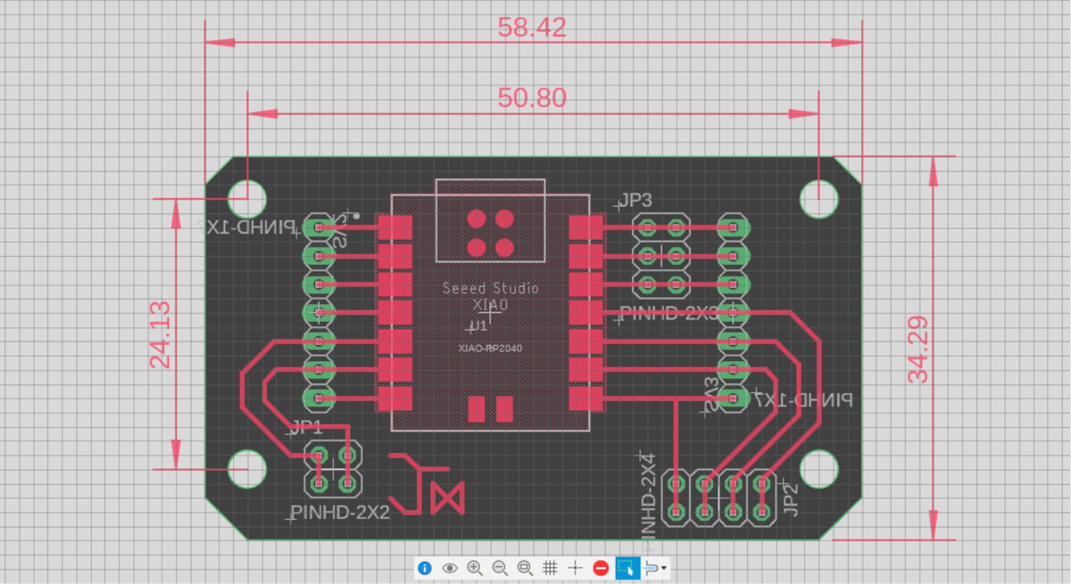 Final project version with dimensions
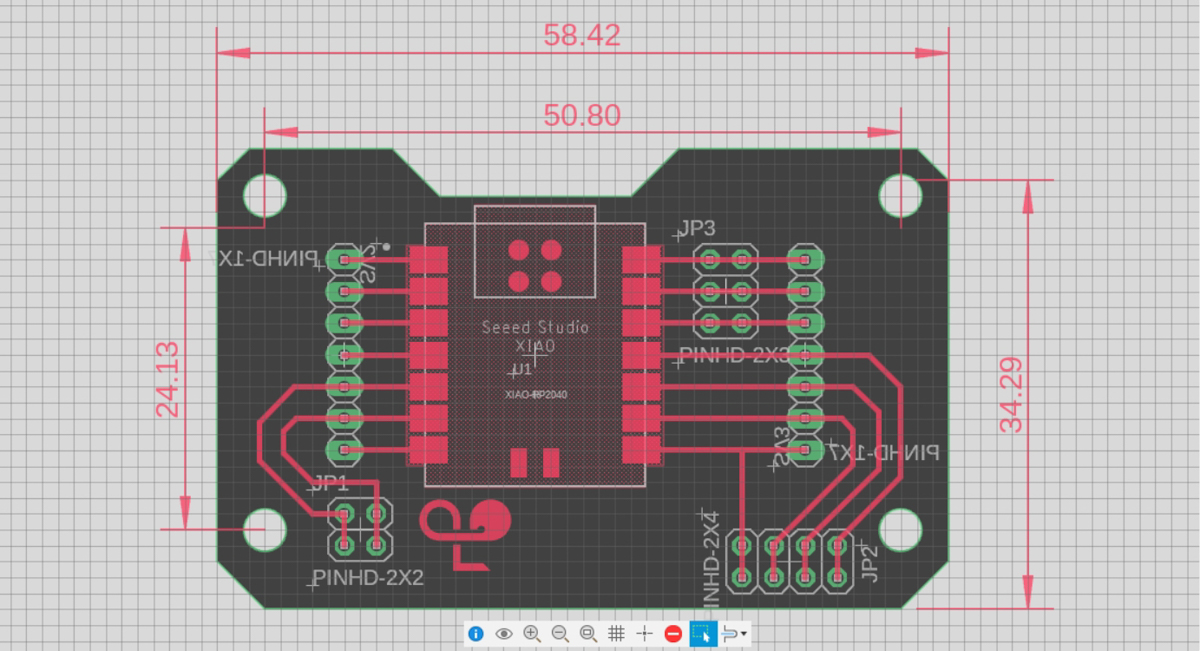 After the final project, another version with better clearances between the pinheaders and the screw holes
I also finally added a personal logo (inspired by Adrian) of my initial letter J but this time it is in the script of my mothertongue Gujarati, and instead of just drawing wires like earlier, I have figured the workflow to make it elsewhere and import the graphic as a DXF, convert it to a polygon and so it appears directly in the copper.
Important Learnings
- The Eagle parts are easier to drag around or even select if you click on the faint crosshairs at the centre of each component
- If components are already connected, whether in the Schematic or in the PCB designer, it makes manipulating them SIGNIFICANTLY more cumbersome
- The easiest workflow is to first add all the parts you want, position them in near-final locations, and then start connecting
- Update design rules before starting out, since it will be more miserable to correct individual parts later
- The Grouping and "Apply to Group" commands are a bit clunky, even though I managed to finally get them to work and didn't have to manually change every wire
SVG PCB
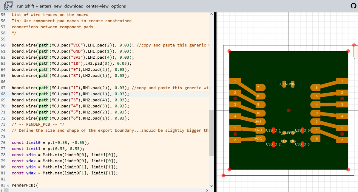
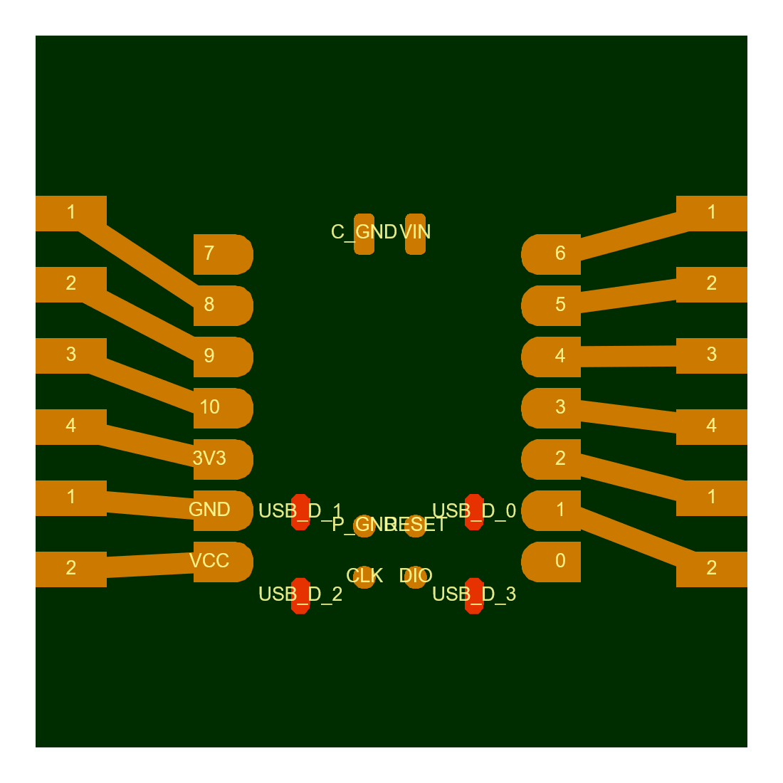
SVG PCB is an interesting workflow, and while I did not make too much headway into it, I managed a basic footprint and some paths. There is a bit of a learning curve, and coding experience helps. I hope to work this out at some point soon. But for now, here's the halfbaked board.
A few more SVG-PCB links that are useful :
KiCAD
I tried my hand at KiCAD as well. However, since I decided to continue with Eagle eventually, I am putting KiCAD on hold for now. One quirk of KiCAD is that a component can have multiple footprints that you have to select/assign yourself. It is an extra step, but also adds a level of versatility. It's a polarizing workflow, to be honest. I was ok with it, but clearly I've gone ahead without it.
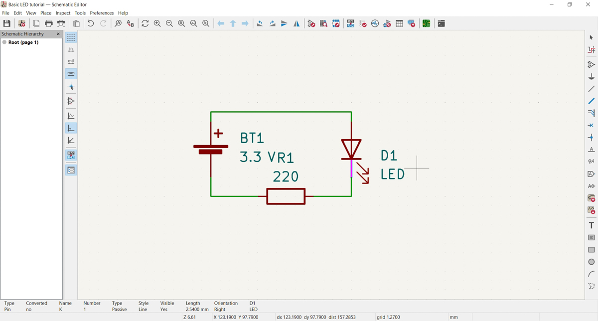
Schematic of LED circuit with CR2024 and resistor
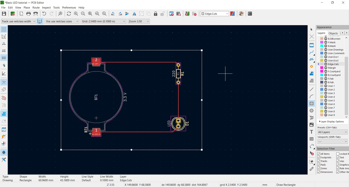
Airwire stage of PCB
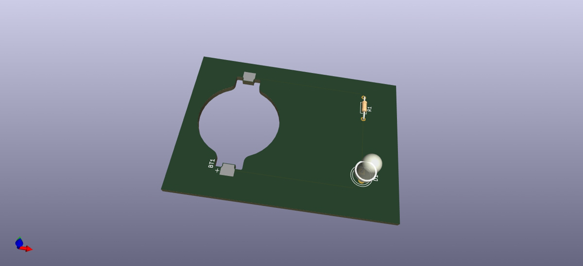
3D view
Detour into SVG-Land
As mentioned earlier, I took off on a tangent for a while since I wanted a particular LED footprint on the PCB. Since I could not find it in a library, I tried various websites and sources, including SnapEDA, but to no avail. However, on SnapEDA as well as elsewhere I found the relevant datasheets. So I finally decided to see if I could simply draw the footprints in CorelDraw and import the SVG version into KiCAD or SVG PCB somehow. This obviously involved another rabbithole detour into SVG definitions and other such. I managed to crawl myself back eventually.
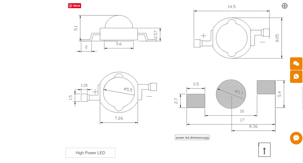 Dimensions in DataSheet
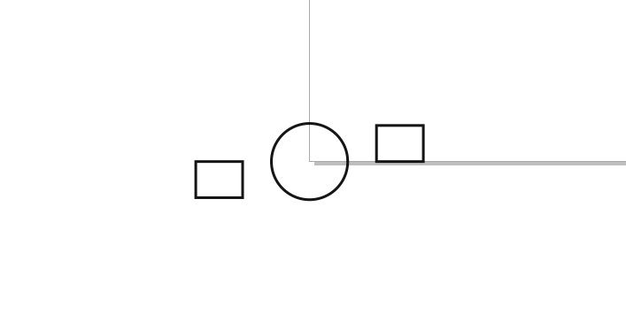 Footprint in CorelDraw centred at 0,0
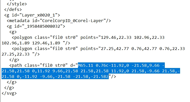 Opening the CorelDraw exported SVG file, and copying the path from there
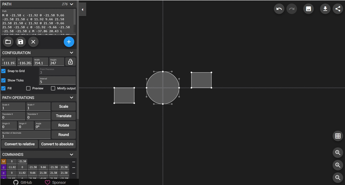
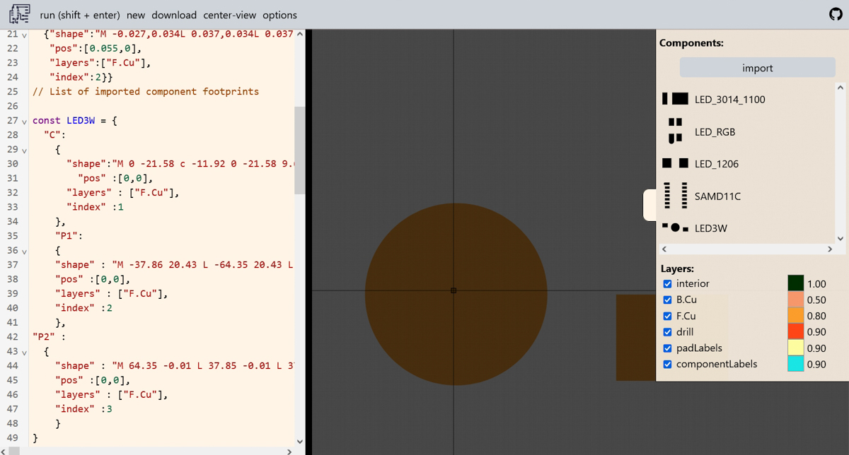 Using the path in SVG Editor as well as SVG PCB
I have not yet managed to figure out custom components and import these into KiCAD/Eagle. The quest continues.
The following links were useful
Custom Graphics/Outlines for PCBs
For future use..
Importing Custom Images into Eagle
KiCad 6 - Importing Complex Board Outlines as Vector Graphics
SVG to Eagle CAD converter
Exercise files
Board File
XIao RP2040 DevBoard v17
Gerber Files
XIao RP2040 DevBoard v7_2023-05-12
XIao RP2040 DevBoard v12_2023-05-31
SVG PCB file
SVGPCB RP2040
