Project
The following pages also add to the account of this project.
Week 17 : Project Applications and Implications
Week 19 : Project Development
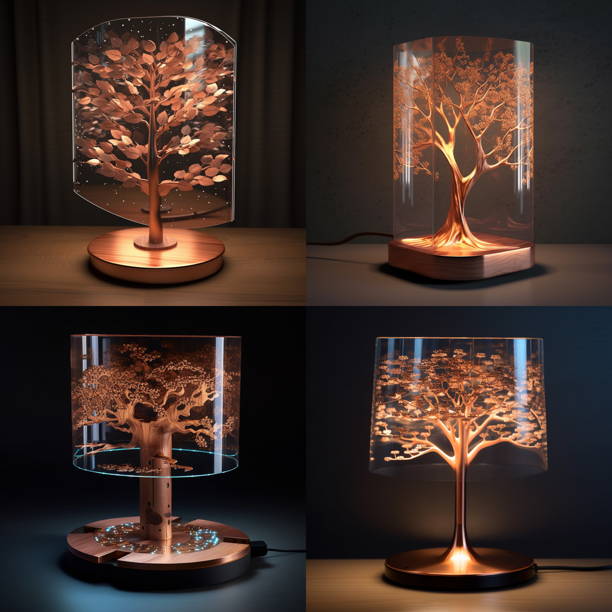
I am fascinated with trees and tree structures. And lamps. So it was rather natural to combine the two - a tree-lamp, of sorts.
PCB milling is the newest skill that I am in the process of acquiring in the course of the FabAcademy, and I want to celebrate and focus on the circuit making end. Ergo, this project is - obviously, and with props to Piers Anthony - going to be called Circuitree.
On the skills side, since I rate myself high on Lasercutting and very low on PCB milling, I am going to try making the main superstructure using a single large PCB milled to shape. As a fallback option as well as for trials, I am also developing a lasercut version. I hope the PCB version works out, but if not, the lasercut version should push through.
On the application side, for one, it's a lamp. /shrug, yes/
It can also have the timer function described in a previous exercise
But mainly, it's a story-teller's lamp.
Trees are central to many legends across the world.
From the Yggdrasil of Norse myth, which held the nine realms, and Odin hung upside down from, to the Kalpavriksha, the wish granting tree, in Hindu mythology. The Bodhi tree under which the Buddha attained enlightenment or the Tree whose forbidden fruit got Adam and Eve cast out of Eden. All these stories, legends, and cultural symbolisms can be mapped to the Circuitree, and we can gather in a circle around this firelight-of-sorts to listen to these stories from across the world.
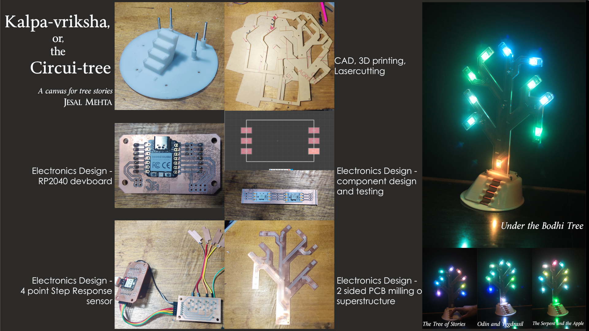
Kalpavriksha, or, the Circuitree
Very initial CAD, not the final


Old Midjourney prompts
A milled PCB / lasercut wire-embedded tree structure with sensors in the base (ideally a series of step response sensors) and a series of neopixel singles on the tree branch ends, to act as an interactive lamp with multiple modes and functions.
An RP2040 in the base acts as the "brains" for this.
Components :
RP2040
Neopixel singles
Step-sensor (created)
Assorted resistors, header pins, etc
Cu wire
Skills and processes :
"Tree" - Lasercutting / PCB milling
Base - 3D printing
Controller - PCB Manufacturing
Input - Step sensor (PCB manufacturing)
Output - NeoPixel singles - lots of code
Initial Sketches
I sketched out the initial concept roughly, and then worked on figuring the structure and directions of the LEDs, which direction they wold face for best effect, diffusers and theier attachment, and the best way to create the path for the power and signal connections.


 I used tracing paper to plot out and understand if I could work this out with a 1-sided PCB, a 2-sided PCB or if I would have to layer more conductive layers somehow.
My conclusion : A branched structure that in essence connected to every LED from the same root would be very convenient for the 5V and GND connections. But the Din and Dout sequence would need to be maintained linearly for addressing the LEDs correcctly. Finally I concluded that it was best to let all the connections be linear in topology instead of mixing things up.
My final wiring can be though of as a long strip that folds over backwards at every branch end and folds towards the front again at every branch junction. (explanatory sketch ?)
Prototype
Based on this conclusion of the topology of the electronics connections, I quickly made a rough prototype from cardboard by hand. I pierced it through and ran copper wire alomng my required path, and the LEDs were glued to their locations.


I needed to do this to
- verify the concept
- verify and completely understand the wire-path topology that would be required for a 2-sided PCB or wired structure
- have an approximate version that I could also start testing the code with
To these ends, the prototype was very successful.
Acrylic version
I had two plans for the superstructure of the lamp, the tree that had the LEDs at the end points and the connections running across it.
The safe and definite option was to embed copper wire into engraved acrylic sheet and run those to make electrical contact. The risky but preferred option was to manage to mill out a large 2-sided PCB and make it work.
I have elaborated on this choice elsewhere in the pages for Week17-19.
For the acrylic version, I had several trials. I did a range of scan settings to determine optimum depth to embed wire, as well as an insanely tedious set of drawings that createed a wire path, holes for the wire to weave back and forth from the acrylic,and LED locations. Trials had told me that embedding wire would loosen up at all the bends in the path, so I created a set of holes so that the wire remained anchored at every point that it had to change direction, andn so on.
After the basic trials and a bad full-size cut, my second full-size cut came out accurate and as intended. I stuck on the LEDs and settled in to weave several dozen meters of wire.


Step Response
I had worked out a single panel Step-Response sensor during Inputs week. Now, based on work done by others as well as some figuring out by myself, I created a 4-point Step Response. I worked out the schematic on paper first, then designed the PCB in Eagle, and making sure the drill holes aligned with the ones in the XIAO DevBoard. I also milled out several PCB pieces to act as touch sensors.


The Step Response board was then connected to the XIAO via Devboard, as well as the touch sensors, and was assembled and tested to determine the best threshold values to code in for a good response. While the code displayed the difference in levels from each pad, since the touch pads were small and quite close together in the final assembly, I decided to finetune the mapping and threshold of the absolute values of the response levels only after it was assembled.
Component Design and Test
While I was using the WS2812B which is a standard component, I was using it in the form of a flexible adhesive strip. I chose this formfactor over single NeoPixels for several reasons.
- the singles have their contacts on the back while the strip units have contacts on the side, making them easier to solder
- the strip comes with an adhesive backing while I would have to figure attachment or adhesion with the singles on my own
- the singles came to Rs 21 per unit (Rs 212/pack of 10) while the strip comes to Rs 8 per unit (Rs 477/strip of 60)
Unfortunately, this seems to be either a non-standard version, or atleast I could not find a datasheet, and more importantly the component footprint, in any of the several libraries I had been using in or added to Eagle so far.
So I decided that it was a simple enough footprint - 6 solder pads, nothing more - and I would figure out how to create custom components in Eagle. Which I eventually did, through a lot of trial and error and trawling the net for various How-Tos, and translating things between the old Eagle (most tutorials use that) and the newer Autodesk-Fusion-Eagle (not many tuts, especially beyond basics).
I'll leave out the actual mind-boggle I went through, but I managed to finally figure out how to create a symbol for the schematic, it's footprint for the PCB design, and attach one to the other to become a single entity available in a library. The component design went through multiple iterations, because I had initially used a far-too-small solder pad size, the location was slightly off, and so on.


 3 versions
 test pieces
 testing with solder paste
Unfortunately, I had made one mistake that was still carried over, which was to assume everything in the world of electronics worked on the 2.54 mm or 100 mils grid system. So while I measured the WS2812b strip and it's solder pad locations, I assumed I was making measurement errors and aligned my design with the 2.54 mm grid. This caused the solder pads to be misaligned - very slightly - along the breadth of the strip. i.e. If the center pad was aligned correctly with the centre footprint, the two pads above and below made ample contact with the footprint, but also were offset enough to potentially make contact with the rest of the copper plane.
This issue was small enough to escape notice, and could generally be ignored on a good day, but became evident later after the main PCB had been milled. At that point, all I could do was be very very careful during the soldering, and while a little nerve wracking, it seems to have worked out.
For the same reason, using solder paste and hot air was not an option since I had to control the solder far more precisely, and so the rest of my soldering was all by hand the traditional way.
PCB Tree
Once I was sure I had the component design workflow sorted, I could proceed with the PCB version that I had envisioned.
My CorelDraw/Fusion drawings would not work, though, because
- the E44 Protomat and it's LKPF software do not accept DXF or any other files, only GBR (we have the Basic Edition.)
- importing the DXF into Eagle was possible but I wasn't too sure of the workflow initially, and once I figured it out, it was still very uncertain and difficult to drag around into position because of Eagle's 2.54 mm grid vs my 1 mm construction
- my Acrylic version was larger than the E44's bed size
The entire thing had to be redrawn and re-networked, but to be fair, Eagle made the job far easier than I had done in Corel/Fusion (as expected) and so I could come up with an entirely new version overnight.
Once we loaded the GBR into LKPF, we realised it's still too large for the machine, since it needs some clearances around for the fiduciary holes. I quickly pushed pulled and dragged the most extreme ends of the PCB closer inwards to accommodate that, and finally the milling was managed.
Since it was a 2-sided PCB, the board had to be flipped around on 2 registration pegs built into the bed of the E44. In an earlier version, I had used an off-the-shelf 2-sided Copper clad PCB and we drilled 3 mm holes to work with the peg, but the alignment between the top and bottom layers weren't good. For round 2, we used the stock sheets that came pre-drilled with the machine to get better fidelity. It worked to a large extent, but I had to be a little careful soldering the header pins because the holes were still somewhat offset.


Oh NO !
Due to the size and position of the PCB on the sheet, the bottom came too close to the registration peg, and while the milling bit cleared it easily enough, the guard around the bit did not. This caused the bit to not be able to dig in completely into the PCB, and left a part of the path unmilled, leading to being connected to the copper plane.

The only solution apart from milling it all over again was to scrape it off manually. It was a small enough section, but I was quite terrified of messing it up. I practiced on one of the test pcbs to see which of the tools I had on hand would work, and how to go about scraping/chiselling/cutting it off.

Once I was surer of how to proceed, I hacked at the main PCB with a small flat screwdriver to correct this. Using a multimeter, I made sure of the connectivity and lack thereof, as needed. Thankfully this part was going to be hidden underneath the top surface in the final construction, so atleast it didn't need to look good.

CAD and 3DP
Once the devboard PCB, the 4x Step sensor PCB and the tree PCB superstructure were ready, only then did I start the CAD.
The beauty of Eagle is even more evident now, since I can export the PCBs as 3D models, tweak them (flipping the direction of several components) and basically use them as components within Fusion360's CAD Assembly of the whole project.

The first thing I modelled was the holding unit for the PCB tree and it's acrylic diffuser/shield layers. I knew I wanted this to be a separate module to be able to repair/replace the entire superstructure of the front and back layers if needed, or if I added resin diffuser layers, etc. It generally made more sense to make the entire tree unit a separate modular entity.


Once the fixed points and constraints were in place - the PCBs, the touch pads, vertical separation to leave space for connectors, etc, I started modelling the enclosure around them. I decided to make the whole thing a sandwich construction so that it would hold all the electronics parts in place between the upper and lower bodies.


Finally, I imported the Tree structure subassembly into the main one, made more adjustments, and corrected a few things to make a sensible assembly sequence possible. Afterall, if this could not be assembled, or needed to be assembled with risk to the more fragile/critical parts, that would not be ideal.

I 3D printed these, cleaned them up and removed the support structures, and started the assembly.


Assembly, Testing and Coding
I initially tested the devboard and code on one of the 2-LED test pieces, and then moved on to the main PCB. I was taking no chances with frying even a single LED.


I had to go back and forth quite a lot because I had decided to use 90 degree headers instead of straight ones to save on height clearance, but this was leading to interference with other areas that I had not anticipated. So I needed and printed several versions of spacers, of varying heights and some with notches or half-cuts to allow for jumper wires and other clearances.


Finally, I started to bring the sandwich assembly together, although I was taking it apart quiet often and altering things as needed.


 had to print a second version since I had taken measurements off a different cable earlier
Once the base assembly was almost done, I brought in the upper module and connected it, then tightened the final nuts in place.


After the complete assembly, I reconnected to the Arduino IDE and tweaked the code further to adjust the step response sensor. I could not pin down a definite value; it kept changing for some reason, I'm guessing that the touchpads were too small, too close and so kept picking up too much influence from each other and my finger. Finally, I simply compared them to each other and realised that while values changed form time to time, the triggered pad always had the lowest value in the system. So I made it that the lowest value would trigger the required functions.


I also added multiple lighting schemas for each of the stories. I wrote myself some quick p5.js code that produced a table of RGB values with the generated colour, to help me select good and convenient RGB values/ranges for the colours I needed for every story.

p5.js sketch for quick reference colour values
The stories and schemas currently added are
a. The Kalpavriksha : the default mode, with random colours being set to each Neopixel but the maximum brightness being limited to 128 (i.e. 50%) for most, while a random few get full brightness to look like bright jewels b. Under the Bodhi Tree : The Buddha, symbolised by an orange light at the base, with the tree Neopixels being set to randomized shades of green c. The Serpent and the Apple : The Serpent being a bright green light at the base, while a randomly selected Neopixel turns to a random shade of red, and the rest of the Neopixels are set to randomized shades of green d. Odin hanging from the Yggdrasil : The left lowermost Neopixel turns blue for Odin, the base light is pure white, and the rest are randomized shades of yellow-green
The Kalpavriksha Revealed

Each step is a touch sensor, triggering a different story.


Assembled and Lit up

The 4 stories

The Kalpavriksha - the wish fulfilling tree

Under the Bodhi Tree

The Serpent and the Apple

Odin hanging from the Yggdrasil
Possible Updates
The assembly, testing and code were functionally complete. However, the following can be added/updated in the future
- Resin diffuser
- Code changes for better triggering
- Neopixel safeguards - capacitor over terminals, resistor before signal 1
- Better fit near front Base
Hero Shots and presentation
License
This work may be reproduced, modified, distributed, performed, and displayed for any purpose, but must acknowledge this project. Copyright is retained and must be preserved. The work is provided as is; no warranty is provided, and users accept all liability.
Acknowledgments
I have generally acknowledged specific people where appropriate along with every weekly exercise, and I also intend to add a general acknowledgments page in the structure for an overall picture. Continuing this, I must express my gratitude to the following groups of people
People whose work I have benefitted from : Adrian Torres, for the grounding in MCUs, Circuit design and Step Response sensors I gained from his work and documentation Akash Badshah's work on the multipoint step sensor
People who have helped me work on this project : Ms Pradnya Shindekar, my Regional Mentor, for guiding me, checking in on me and pushing my motivation when it dropped Mr Sangram from The Somaiya School's Lab, for patiently and diligently helping me over several days with the E44 Protomat and the wild PCB (as well as several other ones) I pushed the machine to make Mr Maitreya from the Somaiya School of Design, my institute, for quick and efficient logistics when I needed materials and equipment Mr Dinesh, also from the Somaiya School of Design, also for quick and efficient logistics when I needed materials and equipment, and the priceless loan of a station that kept my train on track ;)
Exercise Files
CAD files
CircuiTree v16.f3z
CKTree Base v28.f3z
PCB tree pillar spacer v2.f3d
Electronics zip file
project_electronics_files.zip
Contains Board and Gerber files
Code PCB_Tree_StepRGB.ino
Checklist
Week 17 : Project Applications and Implications
Week 19 : Project Development
The above two pages cover the following effectively.
- What does it do?
- Who's done what beforehand?
- What did you design?
- What materials and components were used?
- Where did they come from?
- How much did they cost?
- What parts and systems were made?
- What processes were used?
- What questions were answered?
- What worked? What didn't?
- How was it evaluated?
- What are the implications?
This current page covers the following requirements unless otherwise linked.
- Made your slide> 1920 x 1080 pixels with your name, project name, Fab Lab name, a photo/render/sketch of your project, a brief description of what your project is/does
- Made a ~1 minute (10MB/1080p) video of you explaining your project
- Made a separate Final Project page that briefly summarises your project
- Included the BOM (Bill of Materials) for your project Week 17
- Linked from this page to any weeks that you worked on your final project Week 17
- Linked to your presentation.png and presentation.mp4; make sure they are located to the root of your website
- Included all of your original design files in the archive (2D & 3D, board files & code). No external hosting of final project files - discuss file sizes with your instructor
- Included the license you chose
- Acknowledged work done by others