Project Development
Complete your final project, tracking your progress
What tasks have been completed, and what tasks remain?
The 4x step sensor has already been executed. The devboard for the XIAO was made during the Electronics Design and Manufacturing weeks, so I am using that, but with minor tweaks.
The screw holes on the PCBs have been aligned to be at the same location so they can be screwed down on the same set of bosses.
The superstructure of the PCB tree is the primary task, and that is underway currently.
I am working on two versions concurrently. Ideally I want the superstructure to be a single PCB, but if that does not work out, my fallback option is an acrylic superstructure with copper wire embedded in it.
The rest of my tasks all depend on the superstructure, and will mainly be CAD and 3D Printing. Since I am using my home printer, this isn't a bottleneck.
What's working? What's not? What questions need to be resolved?
The devboard and the step response are working fine.
The Tree PCB is a wild bunch of tradeoffs.
The acrylic version is a definite option that can't really go wrong, but the CAD/drawings/lasercutting files are absolutely tedious to work on, since each LED x3 contacts x2 sides needs to be positioned, and the wire-embed paths need to be drawn accordingly. Also, to keep the wire in position as it wraps around or changes direction, extra under-and-over paths have been added to weave the wire across the acrylic piece.
Pro : Safe and definite
Con : Intense drawing details, intense physical weaving of wires
For the PCB version, on the other hand, Eagle will take care of the paths accurately by virtue of it's function.
However, I have to manually draw everything in Eagle because importing graphics (for the Tree outline) is a bit tedious (I haven't gotten the hang of it, TBH) and in any case, the outline depends on the wire-paths that are a function of Eagle itself.
Due to the topology of the connections, I have to use a 2-sided PCB, and I don't have any vias, etc to connect the two sides. I am simply going to use header pins (sets of 1x3) to jump between top and bottom. This increases my soldering by 3x.
For every LED, instead of 6 points, I need to solder 18 points (6 on the LED, 6 for the before-header top+bottom, 6 for the after-header top+bottom). So, for a total of 10 LEDs, I will solder 10 x(6+6+6) = 180 points, plus assorted ones for supply points, the base junction, and a few others.
Also, since I am designing a custom footprint for the LEDs, the accuracy of that is suspect, although I have done what I can.
Pro : Perfect error free paths, all milled directly without resort to manual intervention
Con : More soldering, risk of errors during design and soldering
On the whole, if the PCB version works, I would prefer to run with that, since a large part of my objective with the project was to deep dive on electronics design and PCB skills.
What will happen when?
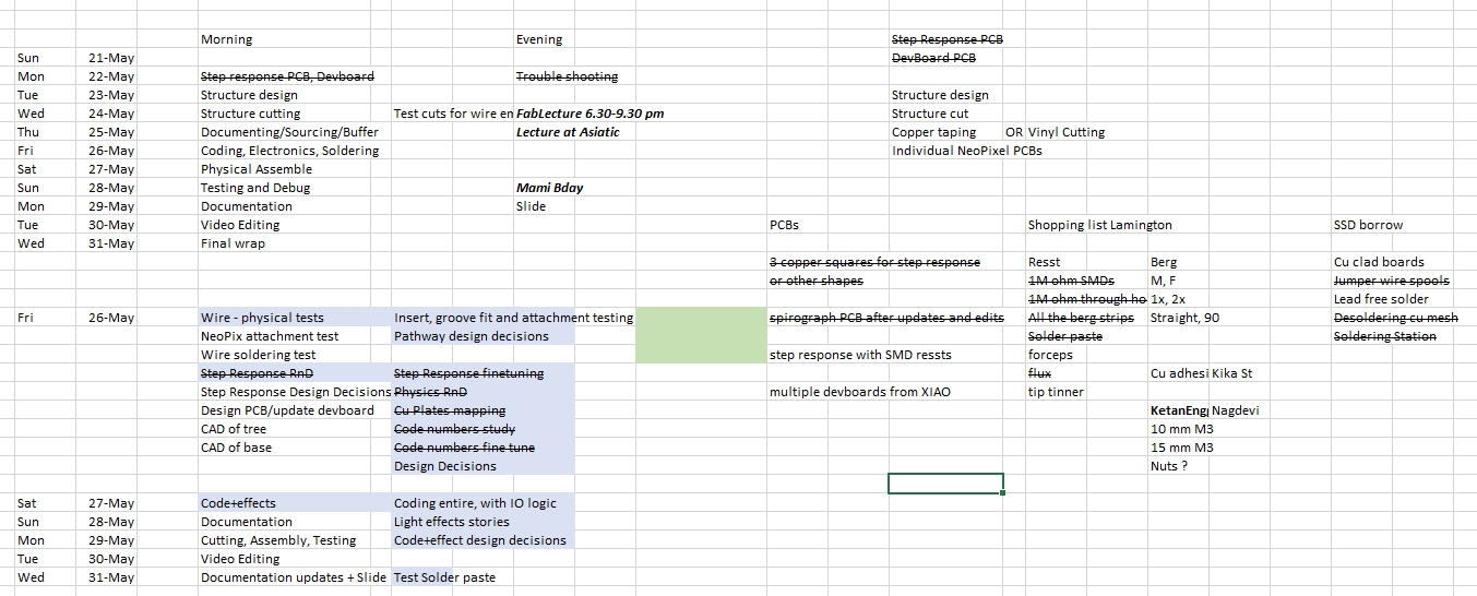
I have been tracking times and tasks in a spreadsheet, and revising them as time goes by.

What have you learned?
On a skillset level
- I have powered through so much electronics design and PCB manufacturing that my confidence in those areas - which I knew nothing about when I started - has gone through the roof.
-
This has also been helped by the fact that I have largely figured this (as well as the rest of the Fab coursework) out on my own, so I am more certain that while stuff will continue to go wrong, I can deal with it, methodically and with the help of all the resources available online.
-
The other skillsets have also obviously improved, every single week. However, I am thrilled by my Electronics progress so I'm not waxing eloquent on the rest of them. Besides, in my opinion, I could have improved my 3D printing or Silicone molding, etc, entirely on my own, but only the push of something like the Fab coursework and structure would have taken me through the entire electronics and digital applications side of things.
On a logistics level
- While I already knew a lot of the suppliers and vendors for the materials used, my regional mentor also helped with a few contacts so I know where to reach out and find specific materials and equipment that may not be otherwise available.
- I have picked up a lot over the years traipsing through the streets of Mumbai, especially the old bazaars, where the areas and markets are organized by what they are offering. So, continuing that same streak during the course of the Fab course, I have become even more familiar with some of these places - especially Lamington road (for electronics), Gulaalwadi (for metal sheets, wires, and tubing), and Kumbharwada (for advanced manufacturing like waterjets and metal lasers)
On planning, procrastination and motivation
- Put down your expected time. Then multiply it by 2.
- I procrastinate until the point where I will HAVE to scramble to get things done. For better or for worse, knowing that I was going to have to pull off quite a bit of work on my own, I actually did plan things better and while everything was still later than planned it was generally on time as required. I have to thank my regional mentor, Ms Pradnya, for pining things down for me and checking in from time to time, keeping me motivated.