
WEEK 06
👉 Individual assignment:
- Design a development board to interact and communicate with an embedded microcontroller
👉 Group assignment:
- use the test equipment in your lab to observe the operation of a microcontroller circuit board 🎯 Click This link for Group assignment page
-
Table of content
Electronics Background
Electronics basics
Electronics components are the basic building blocks of all electronic devices. They are the tiny, intricate pieces that work together to create complex circuits, allowing devices to perform the functions they were designed for. There are countless types of electronics components, each with its own unique function and role in the world of electronics.
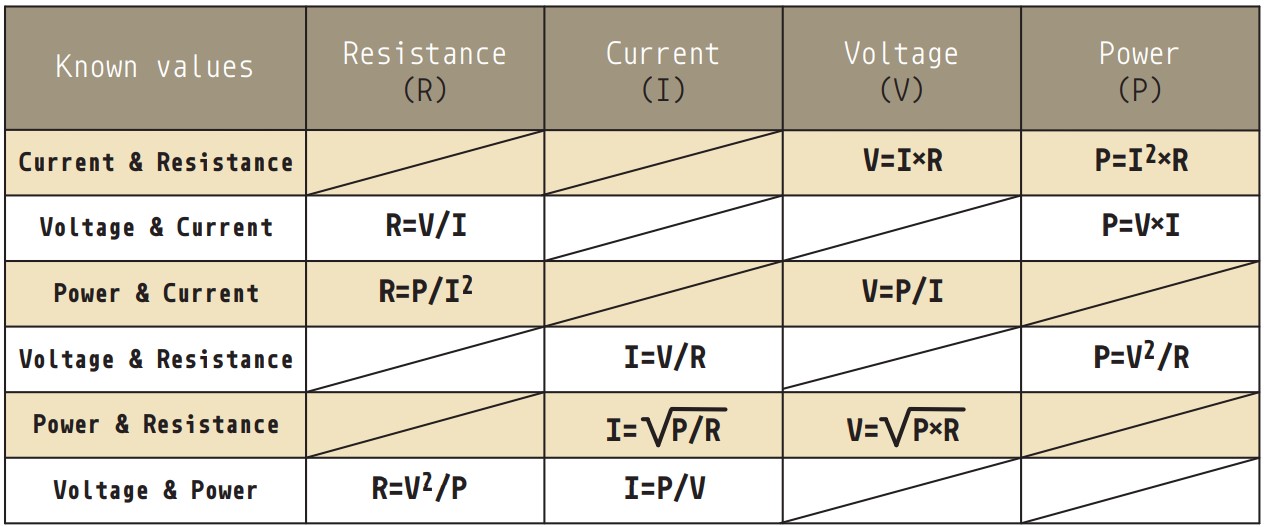
Voltage ? also known as electric potential difference, is the force that drives electric current through a circuit. It is measured in volts (V) and represents the amount of energy that a source, such as a battery or power supply, is capable of supplying to the circuit.
Current ? is the flow of electric charge through a circuit, and it is measured in amperes (A). Current flows from a high voltage point in the circuit to a low voltage point, and the amount of current that flows is directly proportional to the voltage and inversely proportional to the resistance of the circuit.
Power ? is the rate at which work is done, or energy is transferred, and it is measured in watts (W). In an electrical circuit, power is the product of voltage and current, and it represents the amount of energy that is being used or supplied by the circuit. Power is important because it determines how quickly a circuit can do work or transfer energy.
Resistance ? is a crucial term in the study of electricity and electronics. It describes a substance or device's ability to resist the passage of an electric current through it. Resistance is denoted by the letter "R" and is measured in ohms ().
Ohm's Law ? 👈🏼
Ohm's law is a fundamental principle in the realm of electric circuits, which states that the current flowing through a circuit with a fixed resistance is directly proportional to the voltage applied. In simpler terms, an increase in voltage through a circuit with a constant resistance results in an increase in current flow, and a decrease in voltage leads to a decrease in current flow. This law can be expressed through a straightforward mathematical equation.
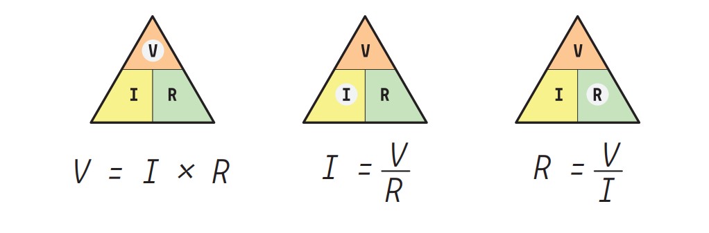
V = I × R
One effective way to internalize the relationship described by Ohm's law is to visualize it using a triangle, commonly known as the Ohm's Law Triangle. This triangle superimposes the three quantities of voltage, current, and resistance, thereby representing the position of each quantity within the Ohm's law formulas. This pictorial representation can aid in easier recall and memorization of the relationship between these three essential components of electrical circuits.
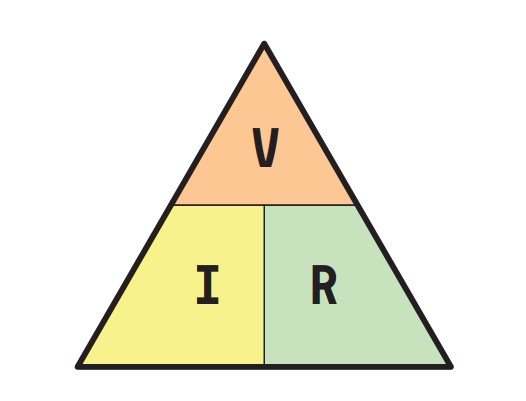
Rearranging the conventional Ohm's Law equation mentioned above yields various equivalent forms of the same equation, such as:
Kirchhoff's Law
Kirchhoff's laws are basic principles used to analyze electrical circuits. These laws describe how current and voltage behave in a circuit.
Here are some Video explanations and Theory about kirchof law .
 https://www.allaboutcircuits.com/textbook/direct-current/chpt-6/kirchhoffs-voltage-law-kvl/

Components
Integrated Circuits
We had already learned about IC’s in week 04
Other components that we will be using this week are Resistor , Capacitor , LEDs .
Follow The below link to access old books on abc connections from ( Alberto Piganti ).
Electronics EDA software ? 🤔
Electronics EDA (Electronic Design Automation) software is a type of computer software that is used by engineers, designers, and hobbyists to design and simulate electronic circuits. EDA software tools are used to create schematic diagrams, printed circuit board (PCB) layouts, and perform circuit simulations.
Following are some of the EDA software's that
- Fusion 360 Eagle Cad.
- KiCad
- OrCAD
- EasyEDA
- Altium designer ( paid )
I'm no stranger to Eagle CAD - I've used it extensively for all my designs. However, I wanted to switch things up and explore new possibilities, which is why I've decided to give KiCad a try. It's always exciting to venture out of your comfort zone and experiment with different tools, and I can't wait to see what KiCad has in store!
I'm no stranger to Eagle CAD - I've used it extensively for all my designs. However, I wanted to switch things up and explore new possibilities, which is why I've decided to give KiCad a try.
KiCAD
The interface of KiCad is generally considered to be user-friendly and easy to navigate, with a range of useful features that can help simplify the circuit design process.
To start a new project Click on
File > New project > ( browse the directory )
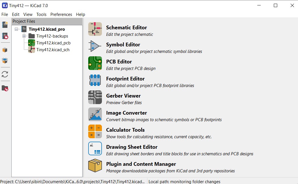
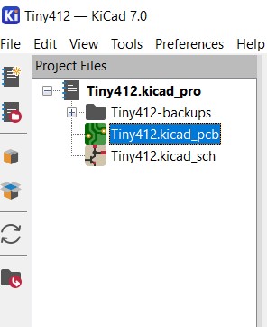
After starting a new project one can see 3 Files created .
My project name is Tiny412
Tiny412.kicad_pcb - is where you create the boards from
footprint.
Tiny412.kicad_sch - is where you create circuit from
symbols .
Circuit Design on kicad
double click on the schematic files from project file
window to open schematic editor
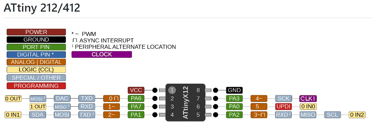
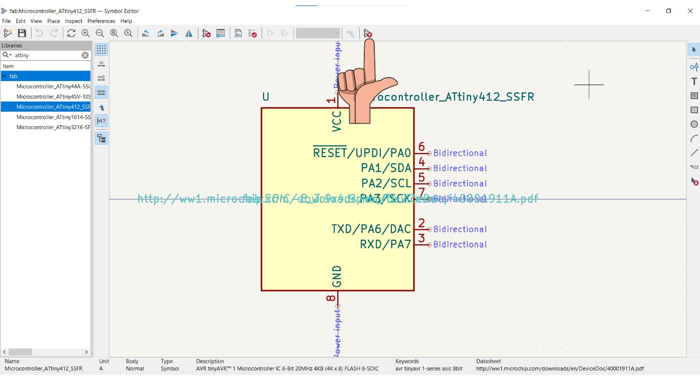
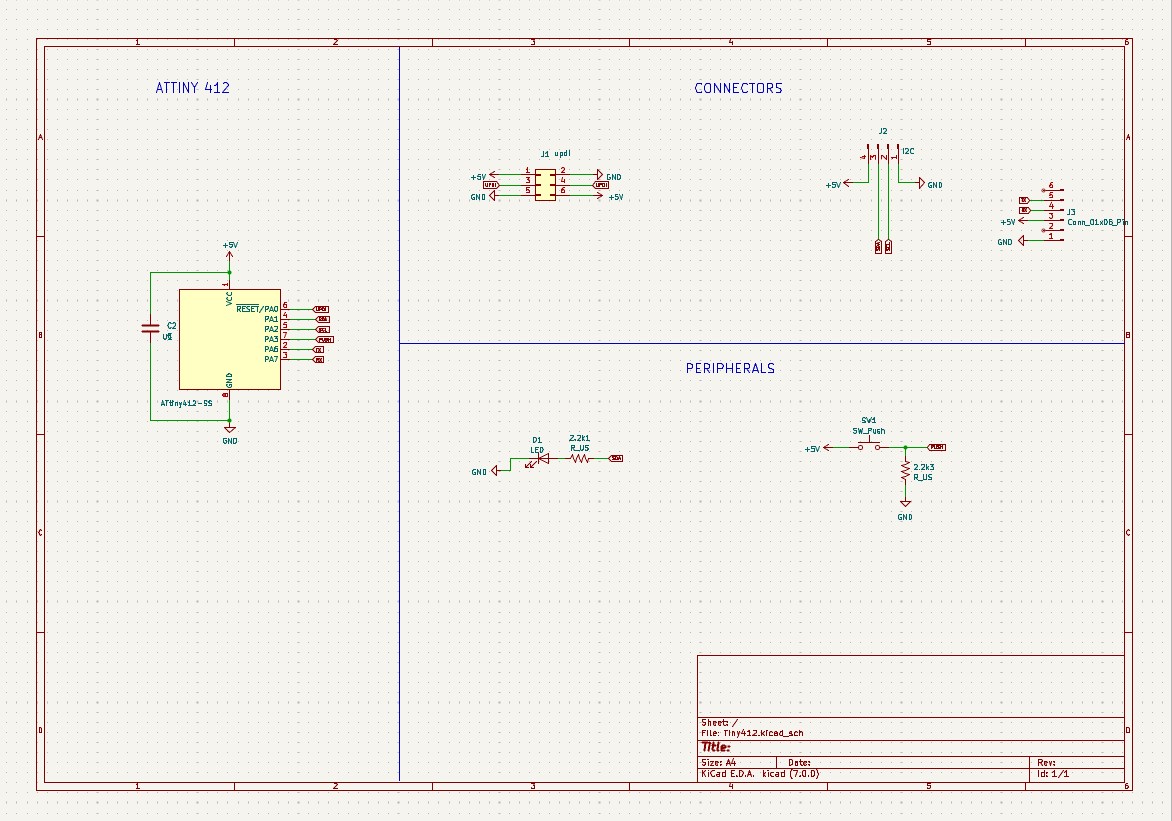
I chose to go with Attiny412 as my microcontroller for the hallo board project.
The Tiny Core Library from spencekonde is a collection of software tools designed to support the ATtiny family of microcontrollers in the Arduino environment. Following link provides a detailed description of the same .
 https://github.com/SpenceKonde/megaTinyCore/blob/master/megaavr/extras/ATtiny_x12.md
Symbol selection
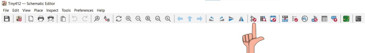
To select symbol Library press the below mentioned icon .
Symbol library - you can search for various component symbols by typing under the search bar in libraries .
After selecting the symbol the the following icon add symbols to schematic .
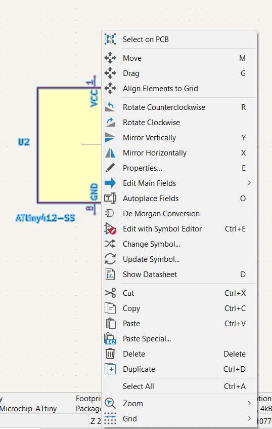
After adding symbol if you right click on the symbol you will get various options and tools to modify the symbol .
Just Like any CAD software you can drag the symbols
around by clicking it with mouse and dragging.
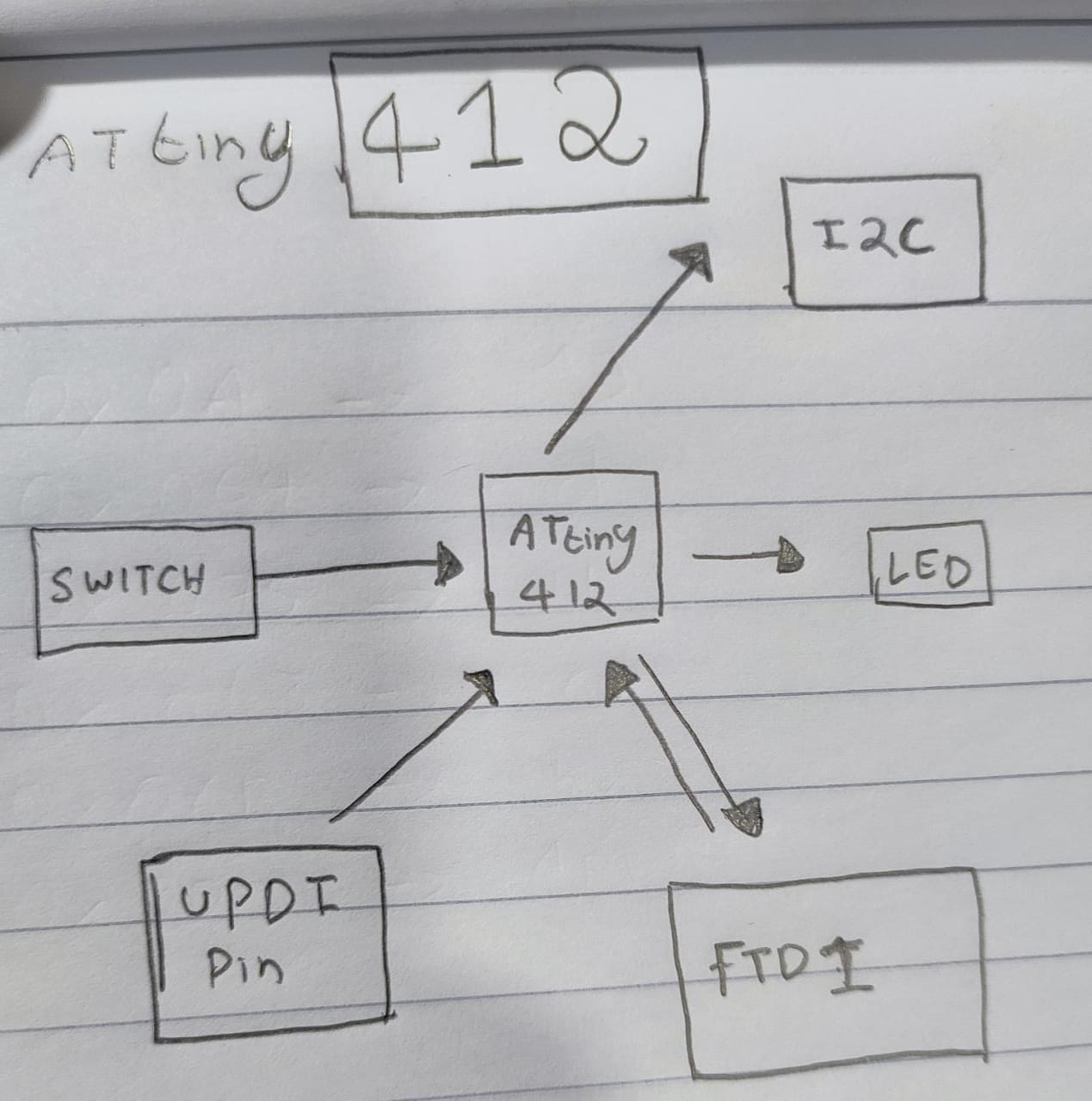
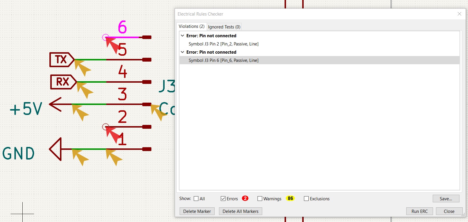
My desired configuration for my Hallo board includes three connectors for UPDI, SERIAL, and I2C communication. Additionally, I would like to have a LED connected to pin PA1 and a push button connected to PA3.
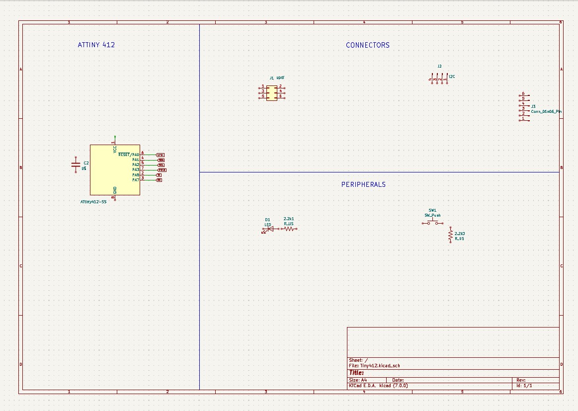
So finally I Placed all the components on my Schematic .
To add separation lines and text click on
place add Lines Add Text .
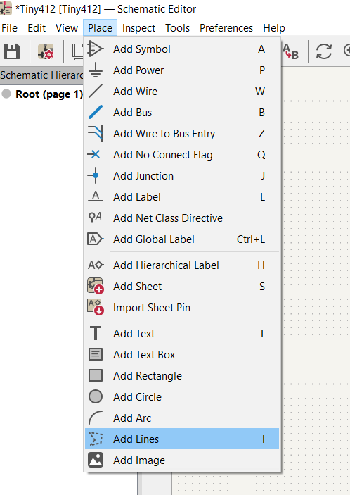
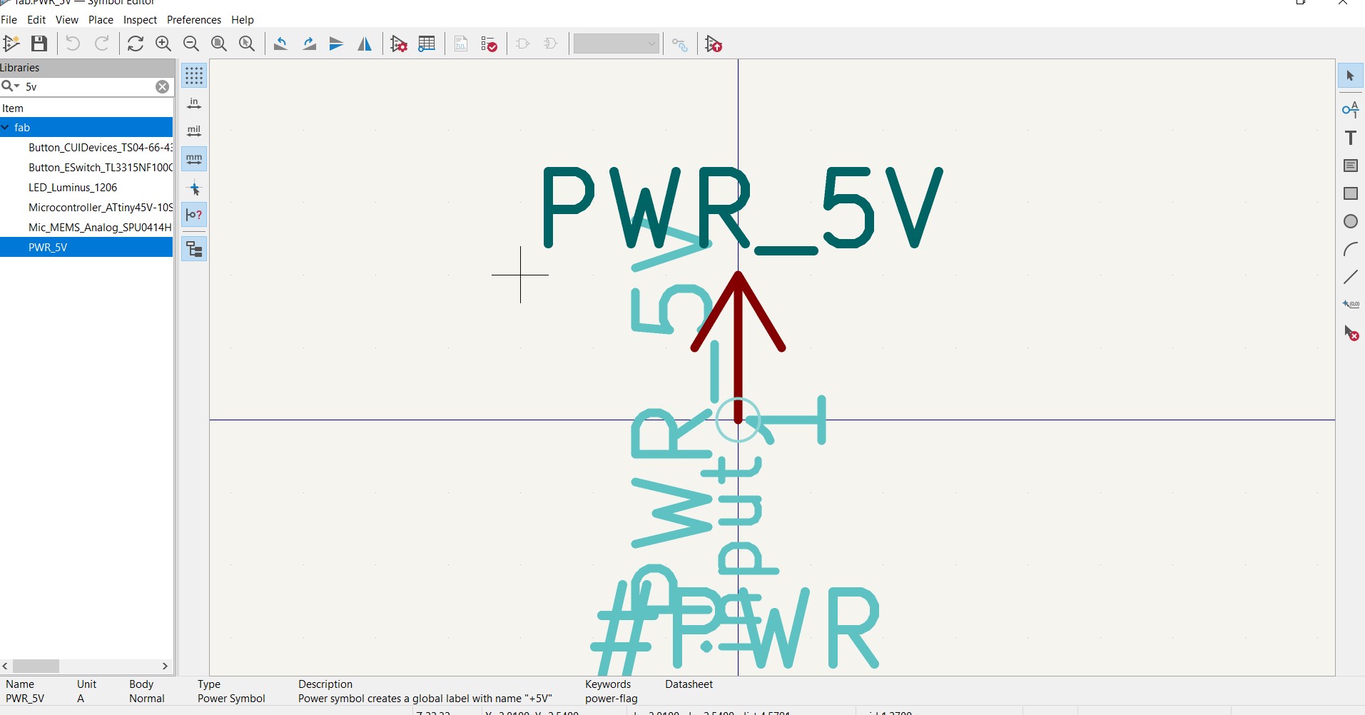
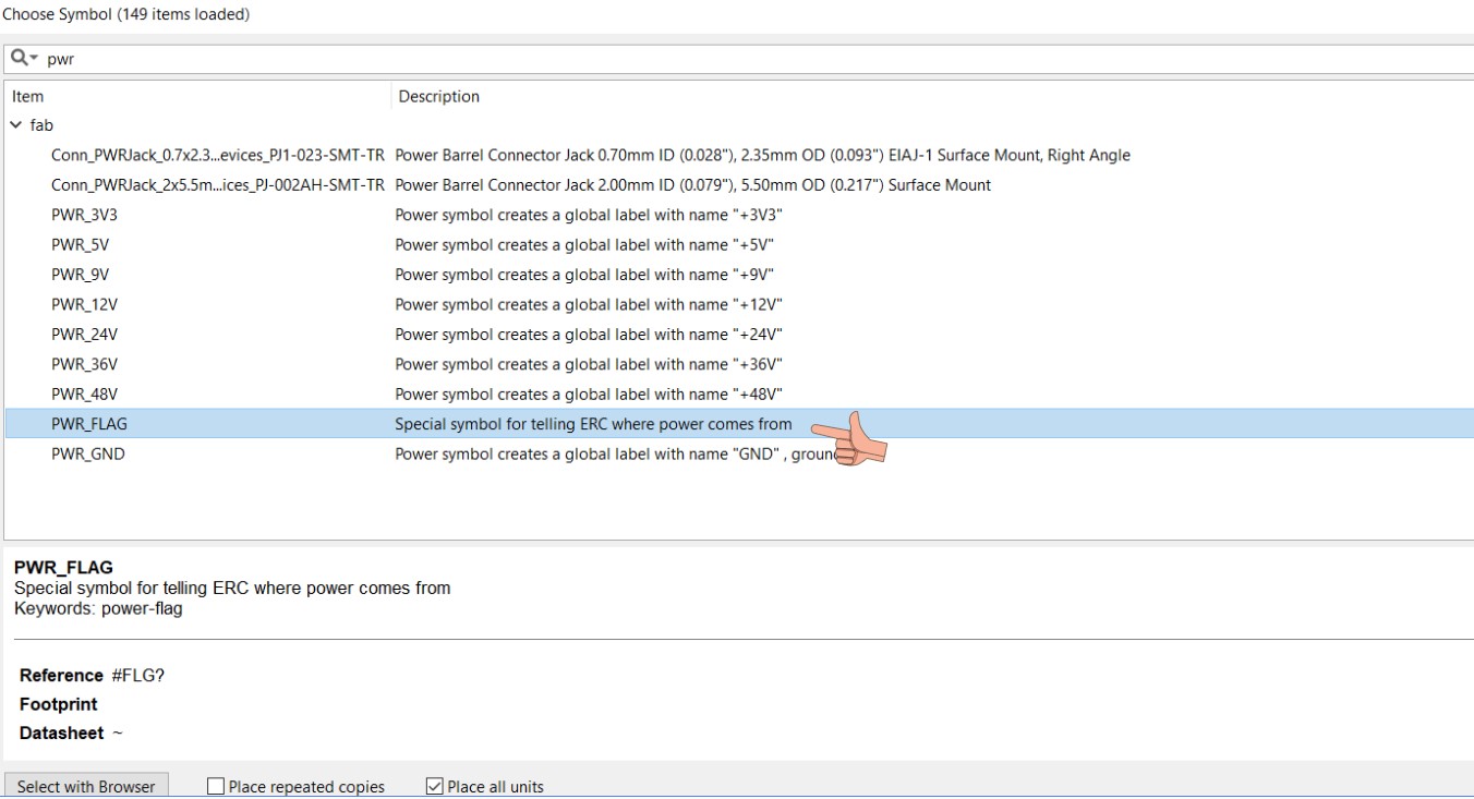
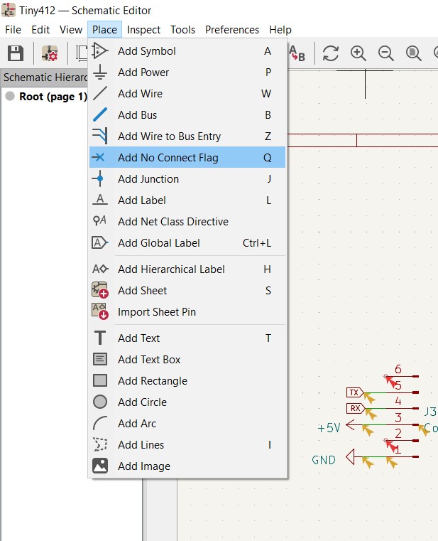
To add power and Ground symbols search for 5V (any power ) and GND .
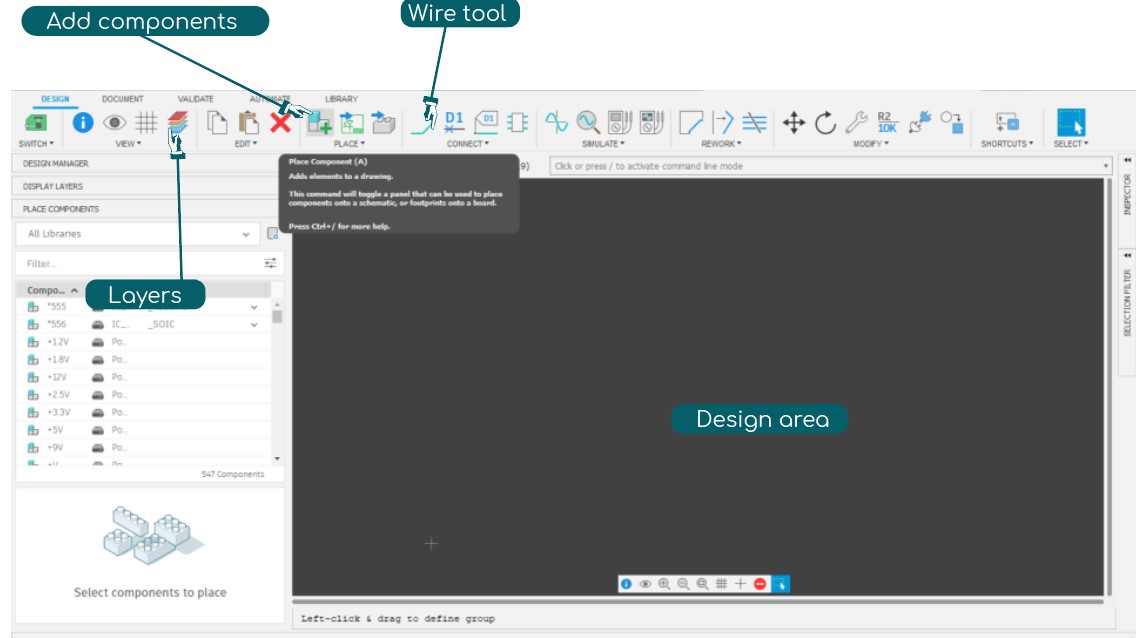
In KiCAD, the wire tool is used to draw connections between the pins of components on a schematic. This tool allows you to create wires that represent the electrical connections between components in your circuit design.
Using the wire tool, you can specify the starting and ending points of a wire by clicking on the pins of the components you want to connect. You can also create junctions by clicking on a point where multiple wires intersect, allowing you to connect multiple wires together.
To select wire tool follow the right tool bar .
How to connect components using wire tool ?
1. Click on the first pin of the component you want to connect, then click on the second pin to create a wire between them.
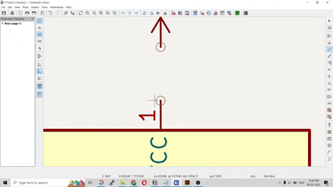
Finally I finished wiring all the component's on my schematic .
what is a Library ? 🤔
library is a collection of electronic components that can be used in a schematic or PCB design. A library typically contains component symbols, footprints, and other related information that describe the behavior and physical dimensions of each component.
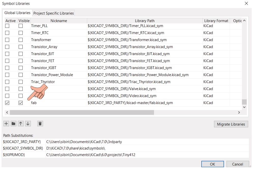
Installing Fab Library on to Kicad.
follow the link to download fab library .

Installation
Make sure you have at KiCad 6 or greater installed.
-
Clone or download this repository. You may rename the directory to
fab.
-
Store it in a safe place such as
~/kicad/librariesorC:/kicad/libraries.
- Run KiCad or open a KiCad
.profile.
-
Go to "Preferences / Manage Symbol Libraries" and add
fab.kicad_symas symbol library.
-
Go to "Preferences / Manage Footprint Libraries" and add
fab.prettyas footprint library.
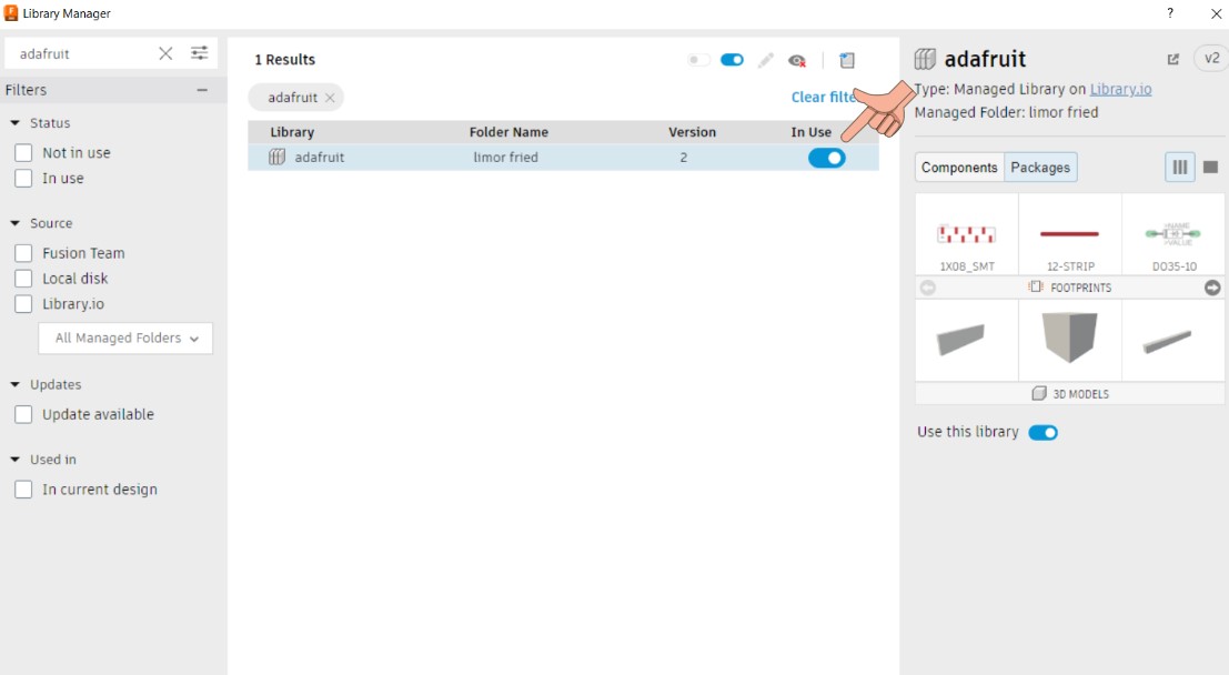
Library manager slection.
-
Go to "Preferences / Configure Paths" and add variable
named FAB that points to the installation directory
of the fab library, such as
~/kicad/libraries/faborC:/kicad/libraries/fab. This will enable the custom 3D shapes to be found. The 3D shapes project has just started and most of them have to be populated still.
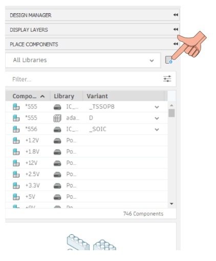
If you just fan fab library and filter out every other libraries you cad do so by deselecting all the other libraries on library manager .
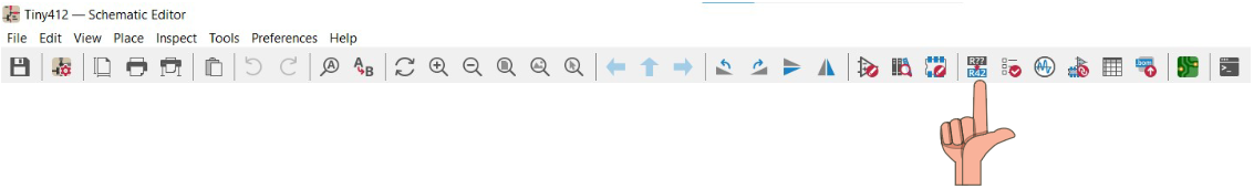
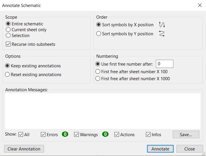
Annotation ?
Annotation in KiCAD is the process of automatically giving each component in a schematic or PCB layout a unique reference designator.
KiCAD adds a default reference designator to each component when you add it to a schematic or PCB layout, such as "U?" for an IC or "R?" for a resistor. When working with larger designs, these default designators' lack of a unique identifier for each component might lead to confusion and mistakes.
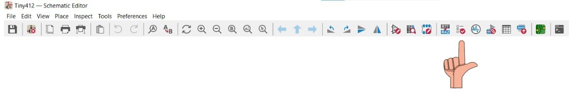
Electrical Rule check
In KiCAD, the Electrical Rule Check (ERC) is a tool that analyzes a schematic design to identify any potential electrical errors or rule violations.
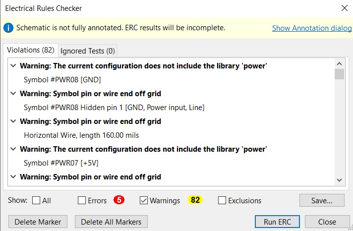
After running ERC I found 82 warnings and 5 Errors 😢
Two errors were detected by the ERC, both of which were related to unconnected pins.
More Warnings 😭
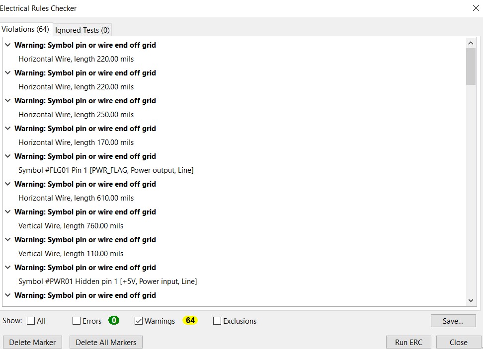
I was still left with
62 warnings .
“symbol pin or wire end of grid” I couldn't find any
resolutions to this warning so I decided to ignore these flags.
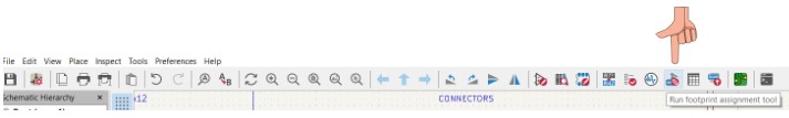
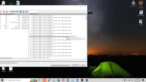
Footprint Assignment
A footprint assignment refers to the process of selecting a specific physical footprint for a component which is placed on the schematic .
When designing a PCB, it is important to select the correct footprint for each component to ensure that it fits properly on the board and is correctly aligned with other components. KiCad includes a library of footprints for commonly used components, but users can also create custom footprints if needed.
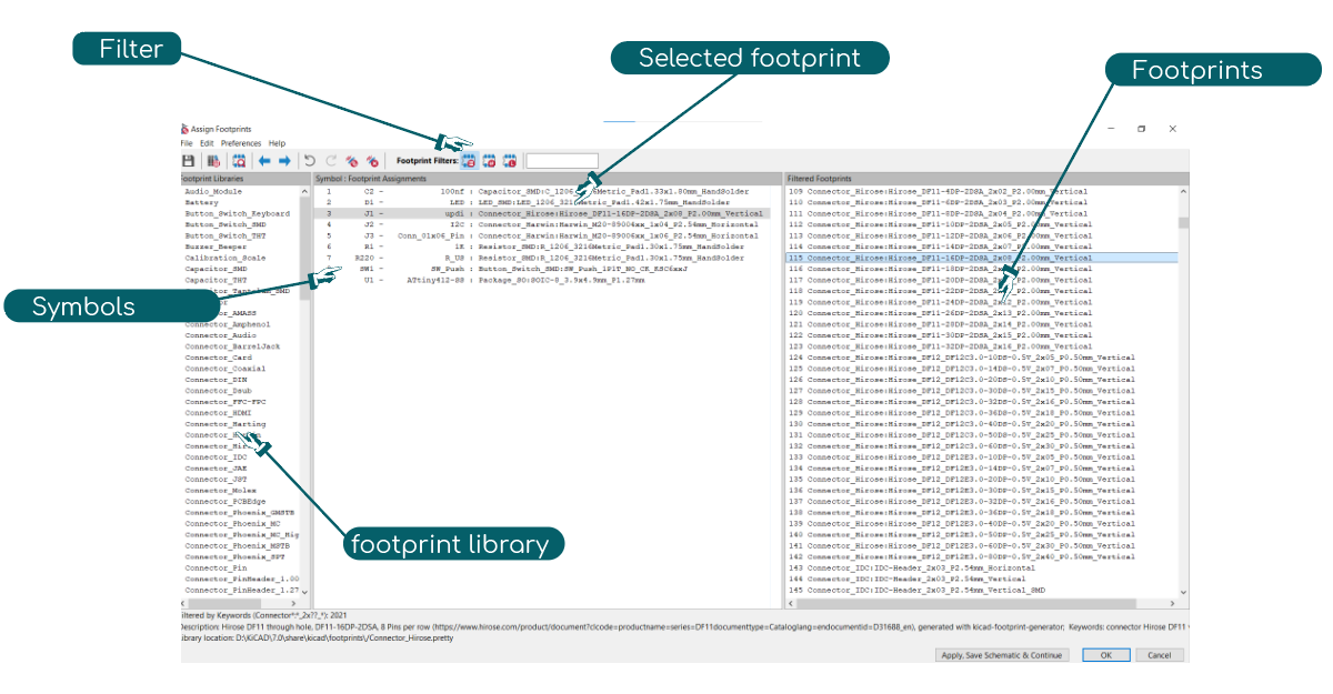
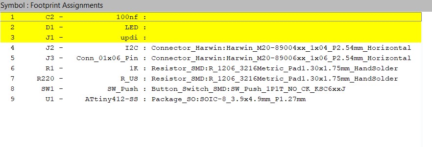
In foot print assignment tool you can choose a pre-existing footprint from the library or create a new one. To choose an existing footprint, click on the symbols which is highlighted in yellow ( un assigned symbol) and navigate to the library where the footprint is located using the search bar to find the footprint by name or by keyword.
To view the selected footprint right click on the foot print and
select “view selected footprint”
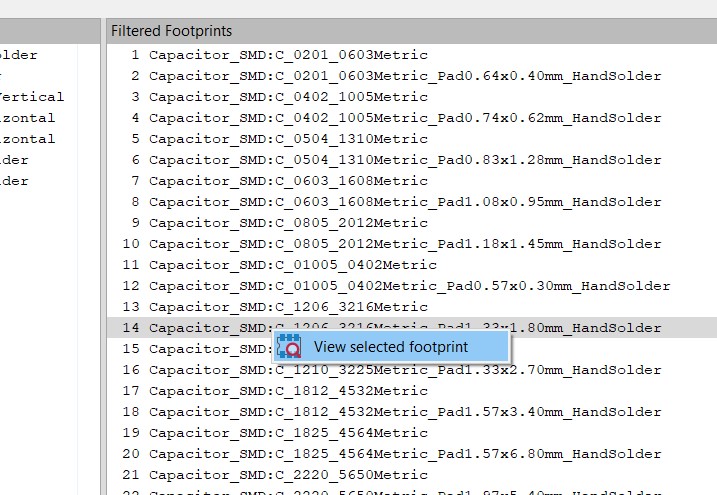
To view various foot prints scroll through the selection while foot print viewer windows is on .
After assigning foot print now its time to create the board .
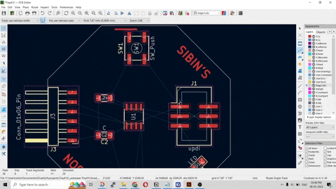
Board editor
Now its time to create the board from foot print .
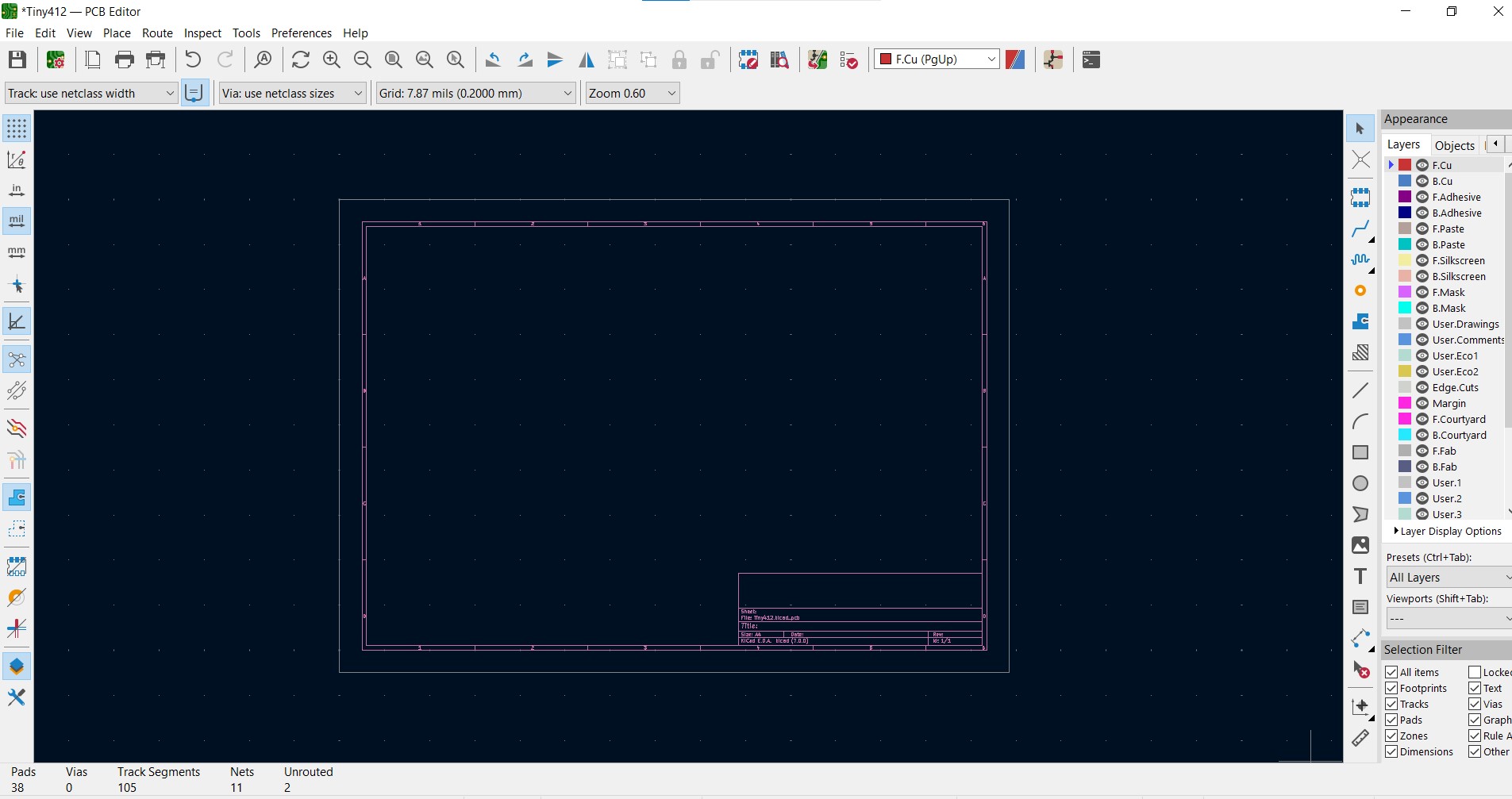
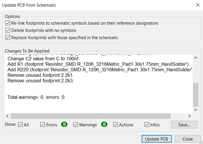
Click on the update pcb icon to load pcbs from schematic .
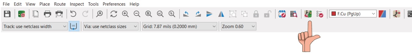
Click “update PCB” to load footprint to board
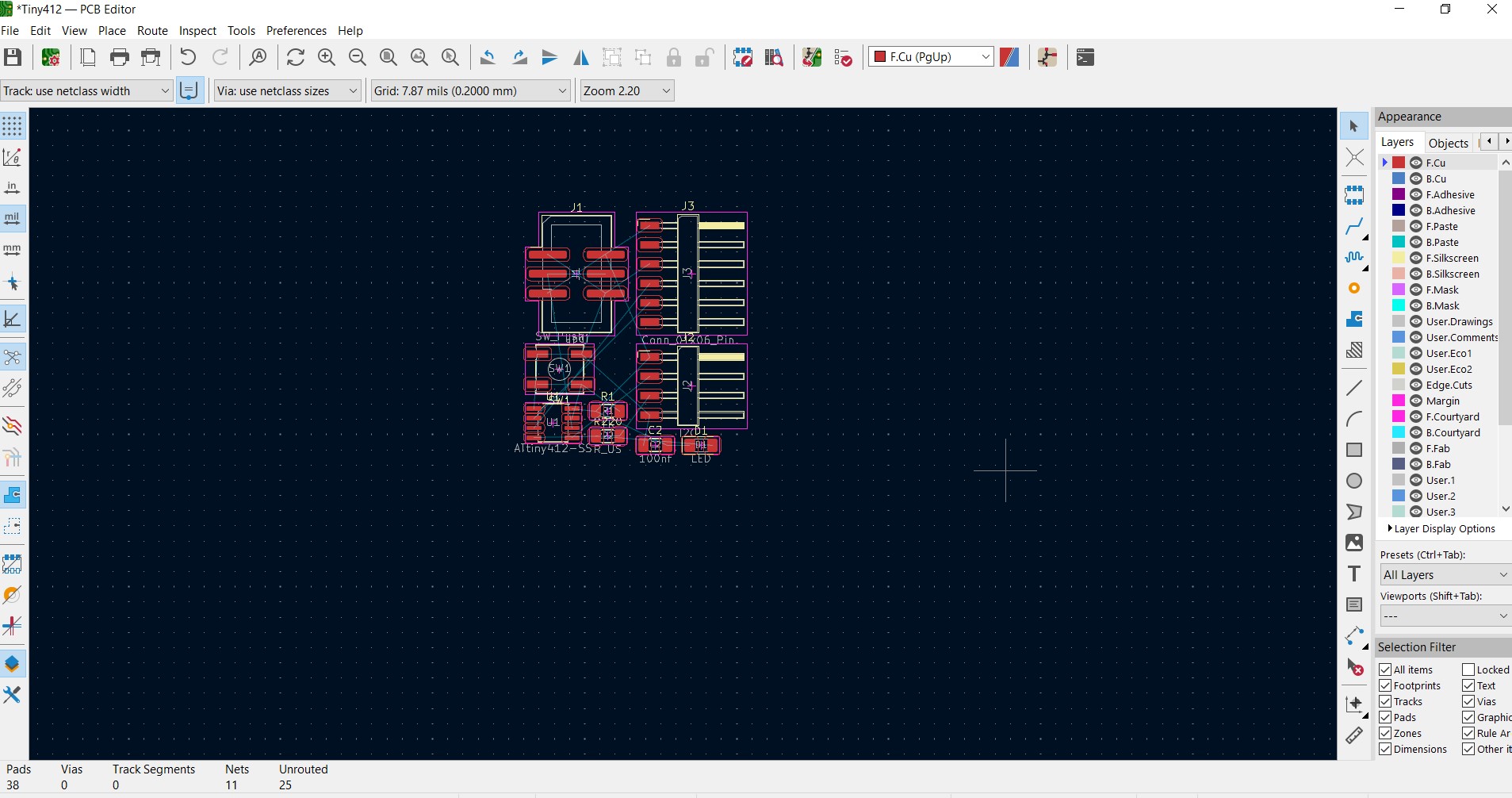
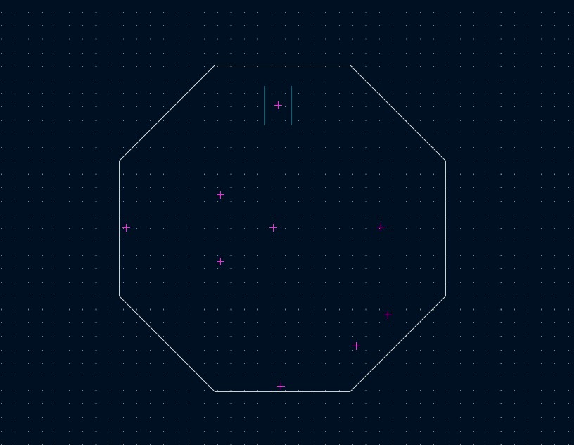
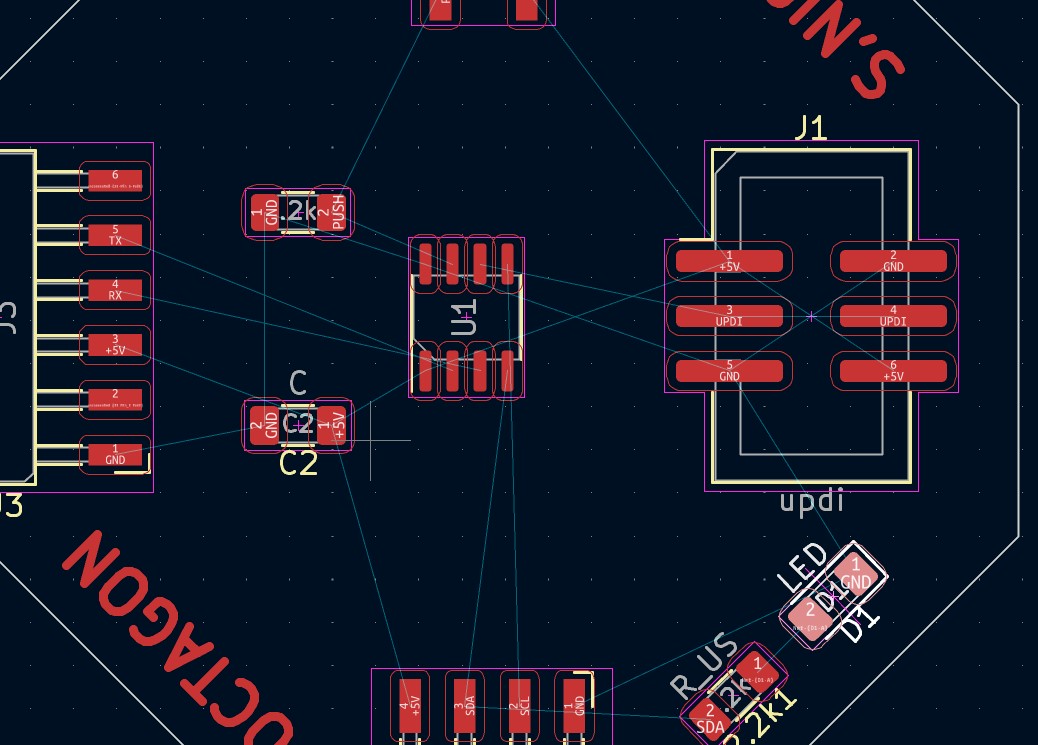
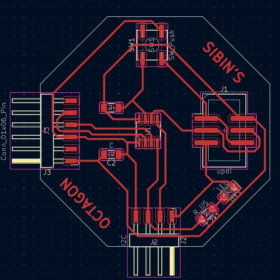
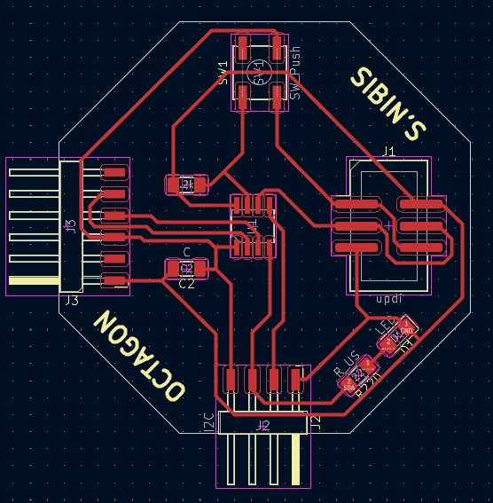
I decided to draw an octagon outline (edge) for my pcb
To draw lines, you can utilize the line-drawing tool
located on the toolbar on the right-hand side of the screen.
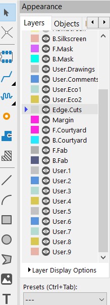
edge cut in layers for pcb outlines
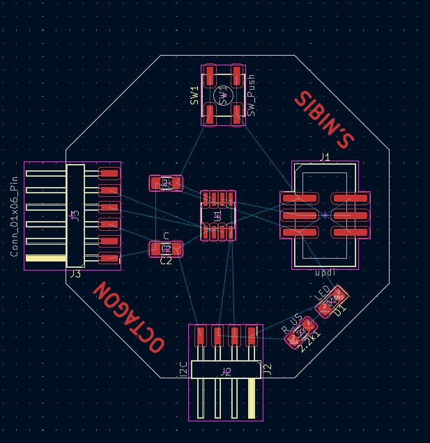
I arranged all the components inside the octagon . To write text
select the Text tool from right tool bar.
orientation value to rotate.
Now its time for wire all the components .
Airwire ?
In KiCad, an airwire refers to a visual indication of a net connection that has not yet been routed between two pins or pads on a printed circuit board (PCB).
When you place a component on a PCB layout, KiCad automatically generates airwires that represent the net connections between the pins or pads of the component. These airwires appear as thin lines that connect the pins or pads and are color-coded to indicate the net name.
Once you begin routing the net, the airwires will disappear as the actual traces are created. However, if a net remains unrouted, the airwire will persist, indicating that the connection is still incomplete.
Airwires are useful for visualizing the connections between components and for keeping track of which nets still need to be routed. They can also be used to locate unrouted connections that may have been missed during manual routing.
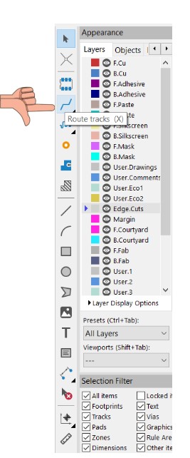
Track width : In KiCad, track width is the same as trace width. Both terms refer to the width of the copper conductive paths on a printed circuit board (PCB) that connect the various components on the board. The width of a track or trace affects the ability of the PCB to carry current and its resistance.
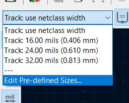
Press the edit-pre defined sizes to add more tracks .
Design rules
In KiCad, design rules are a set of parameters and constraints that define the physical and electrical properties of a printed circuit board (PCB) design. These rules help ensure that the design meets the minimum requirements for the manufacturing process and that the final PCB functions as intended.
The design rules in KiCad cover a wide range of parameters, including trace width and spacing, clearance between components, via size, drill size, and many other factors.
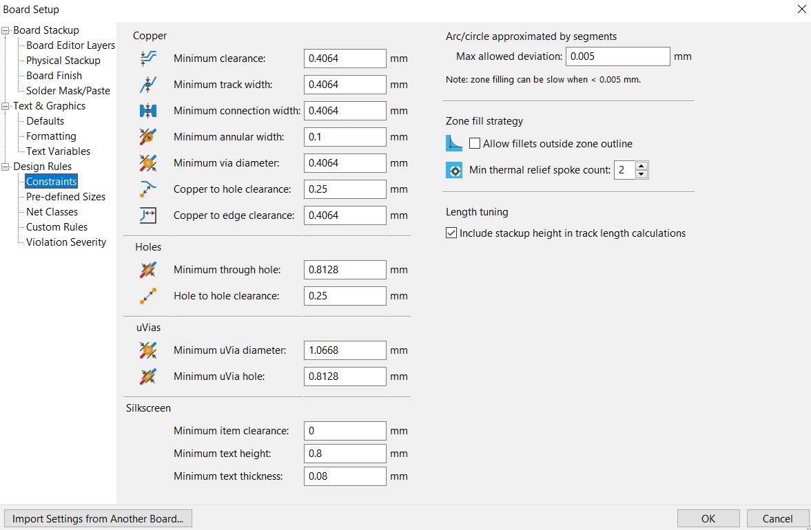
Give the necessary constraints - generally given with respect to the manufacturability or constraints of the manufacturing machine process .
Wiring
To connect two wire trace for two components select the pad from one component and follow the air wire to the pad of other component .
"I've just wrapped up my design, and while it took some effort, I'm thrilled with the outcome!” 😃
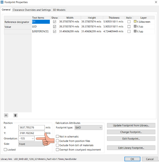
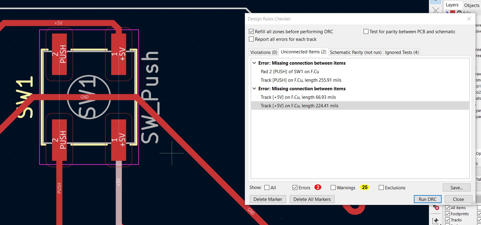
I had two errors for my push button for unconnected pins . I chose to ignore it since physically the pins were connected externally inside the button.
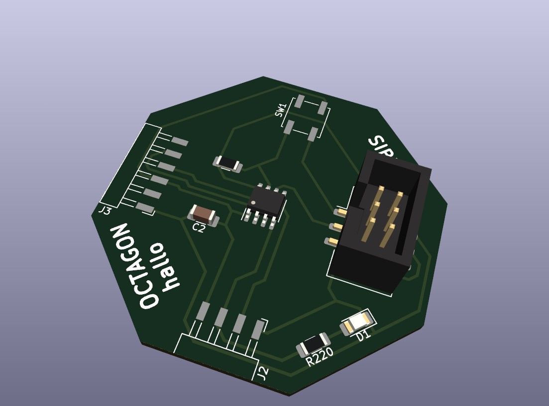
3D view
In KiCad, 3D view is a feature that allows you to generate a three-dimensional representation of your printed circuit board (PCB) design. This feature uses data from the board layout and component models to create a realistic 3D view of the PCB, including the placement and orientation of all the components, and the traces and vias that connect them.
To view 3D click on view and select 3d viewer .
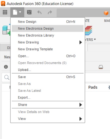
Fusion 360 and Eagle Cad
I used to work on eaglecad for most of my EDA designs . Now Autodesk has integrated Eagle CAD into Fusion 360, allowing users to design their printed circuit boards (PCBs) directly in Fusion 360 and import them into Eagle CAD for layout and manufacturing. This integration makes it easier for users to move between the two tools and provides a seamless design experience. Additionally, Fusion 360's 3D modeling capabilities can be used to create enclosures and other mechanical components for use with Eagle CAD-designed PCBs.
To Open new electronic design click on
files .
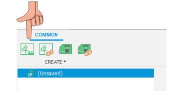
To a new schematic click on the following icon .
Schematic editor opens
To open library manager click on the following icon
Basic library that i like on eagle cad.
Adafruit library - Adafruit EagleCAD library is a collection of electronic component symbols and footprints designed for use with the EagleCAD software. The library is developed and maintained by Adafruit Industries, a popular manufacturer of open-source electronic components and kits.
SparkFun EagleCAD library is a collection of electronic component symbols and footprints designed for use with the EagleCAD software. SparkFun is an electronics manufacturer that specializes in creating open-source hardware and software, and their EagleCAD library is one of their most popular offerings.
follow the link to install both libraries
 https://www.autodesk.com/products/fusion-360/blog/library-basics-install-use-sparkfun-adafruit-libraries-autodesk-eagle/
Use the search button to find libraries .
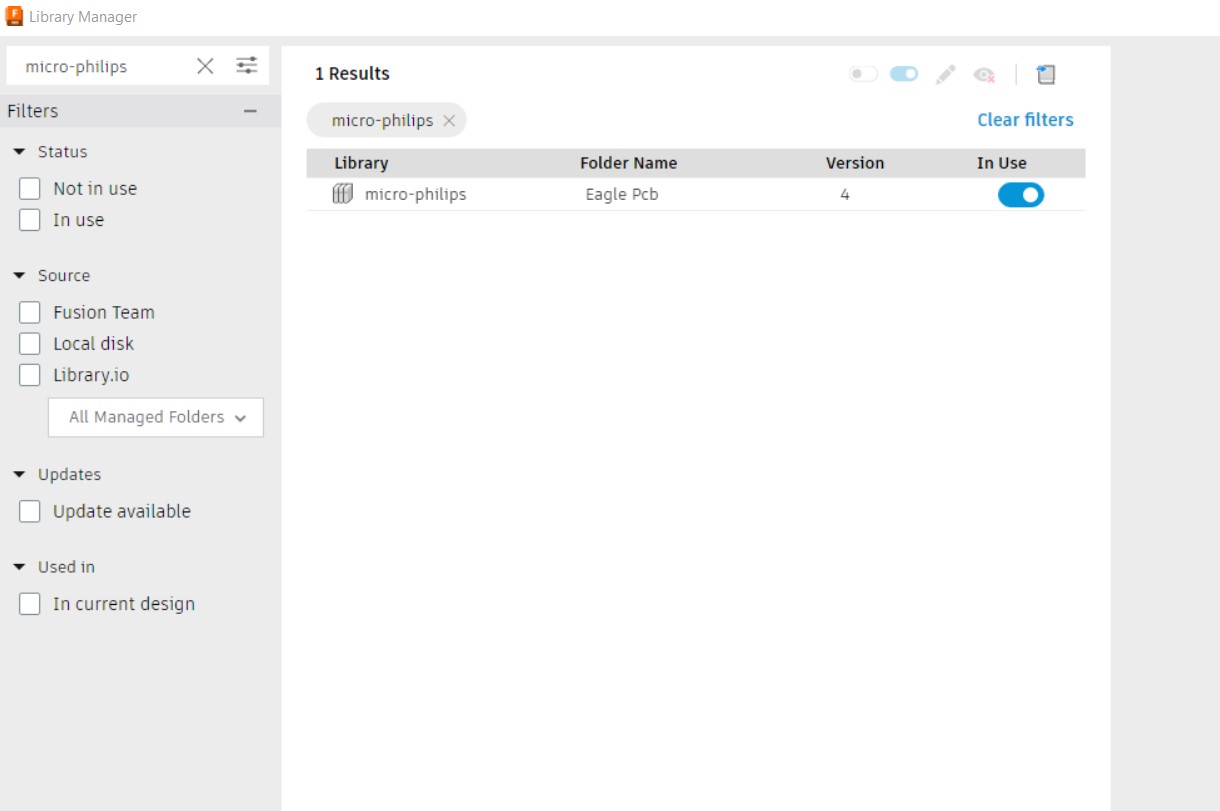
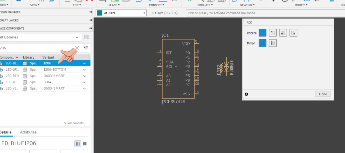
I wanted to place PCF 8574 but I count find it on fusion .
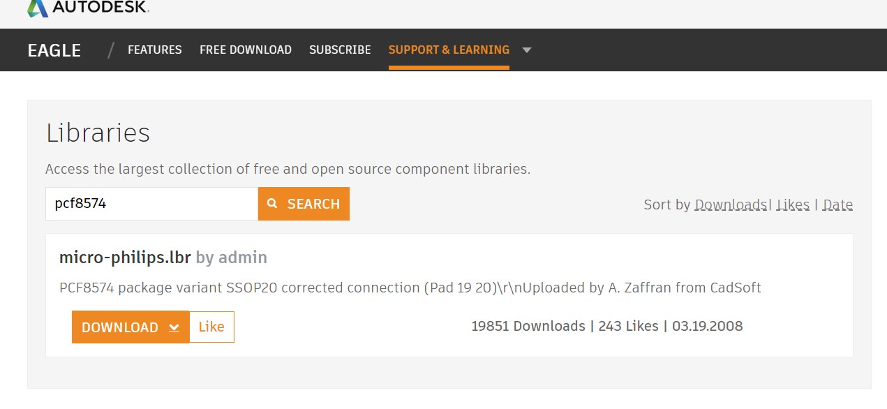
I discovered that the Micro-Philips library contains that component, and subsequently added the library to my Fusion project.
To add a component Click and drag the component onto the schematic editor window. The component should appear as a symbol on the schematic.
If the component does not appear to be the correct size or orientation, you may need to rotate or resize it. To do this, select the component and use the "Rotate" or "Scale" tool in the toolbar.
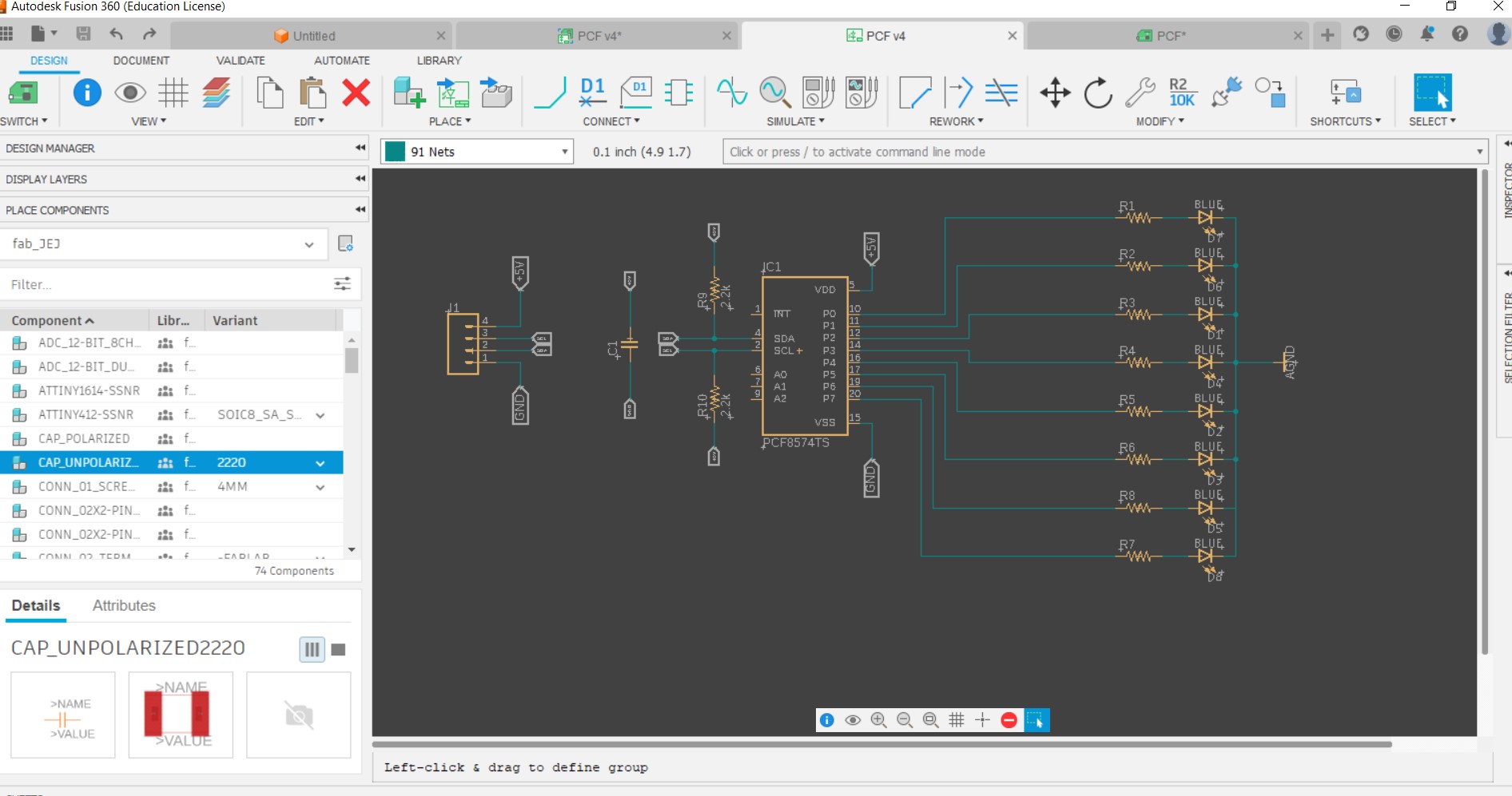
Finally I completed the design
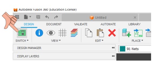
To move on to board design press the bellow icon under
switch .
Auto routing
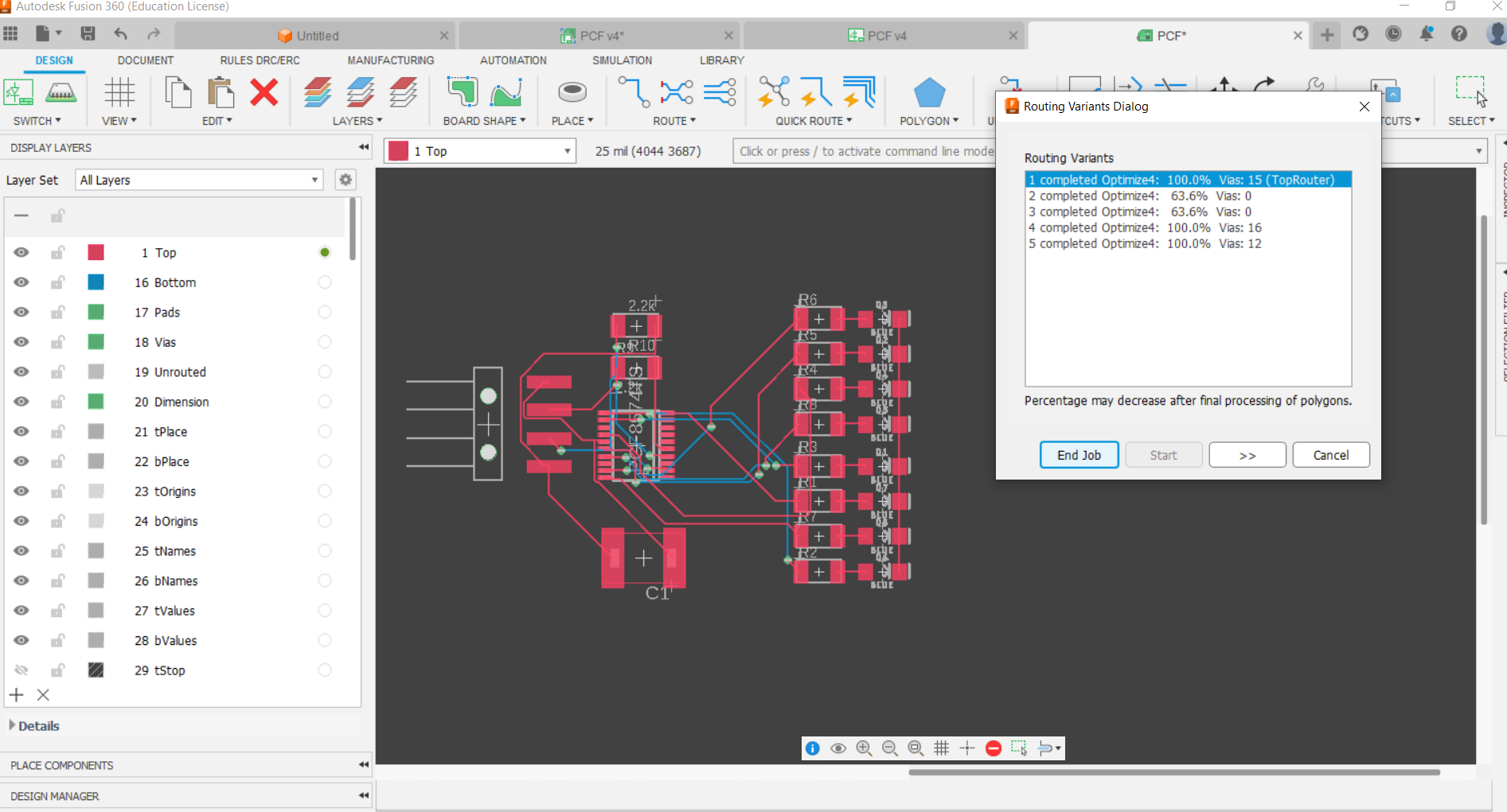
To select auto routing take auto route from
quick route menu .and click start
Autorouting in Fusion 360 is a feature that automatically generates a PCB trace layout based on a schematic design. It is a tool that simplifies the process of designing a printed circuit board (PCB) by automating the routing of electrical connections between components.
When autorouting is enabled, the software automatically generates the routing for all the connections in the schematic, based on a set of routing rules defined by the user. The routing rules define the width of the traces, the spacing between them, and other parameters that affect the electrical performance of the PCB.
Autorouting can save time and reduce errors by automating the tedious process of manually routing each connection on the PCB. However, the quality of the resulting layout can vary based on the complexity of the schematic and the specific routing rules used. In some cases, manual adjustment of the routing may still be necessary to achieve optimal performance.
Resources and Downloads 📩
📩 Kicad PCB file Attiny 412📩 Kicad Schematic file Attiny 412
📩 Fusion 360 8574 File