8. Electronics Production
This week we learned how to manufacture a PCB board.
Group work
In our group work, we milled the board with Roland SRM-20 milling machine. Roland SRM-20 is quite accurate, however, it requires extreme care from the operator for the initial positioning. The positioning of the drilling blade along the Z axis also requires attention since it can either crash to the surface if it is lowered too much, or may not drill the board if it is located too high. Overall, I would prefer to use an LPKF machine for drilling my PCB boards.
Exporting Gerber X2 file from KiCad for PCB manufacturing by LPKF machine.
I started with the following PCB layout design built in Kicad in Electronics Design Week (Figure 1):
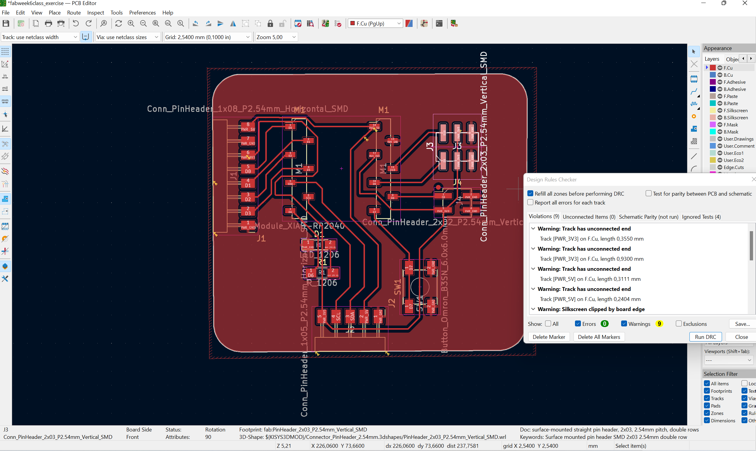
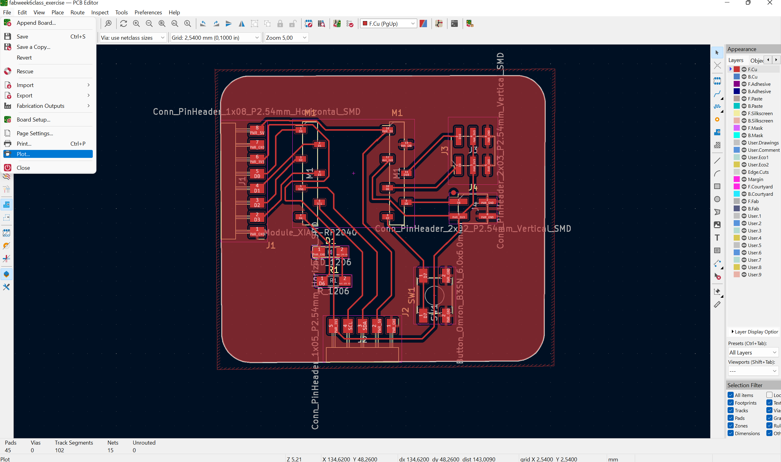
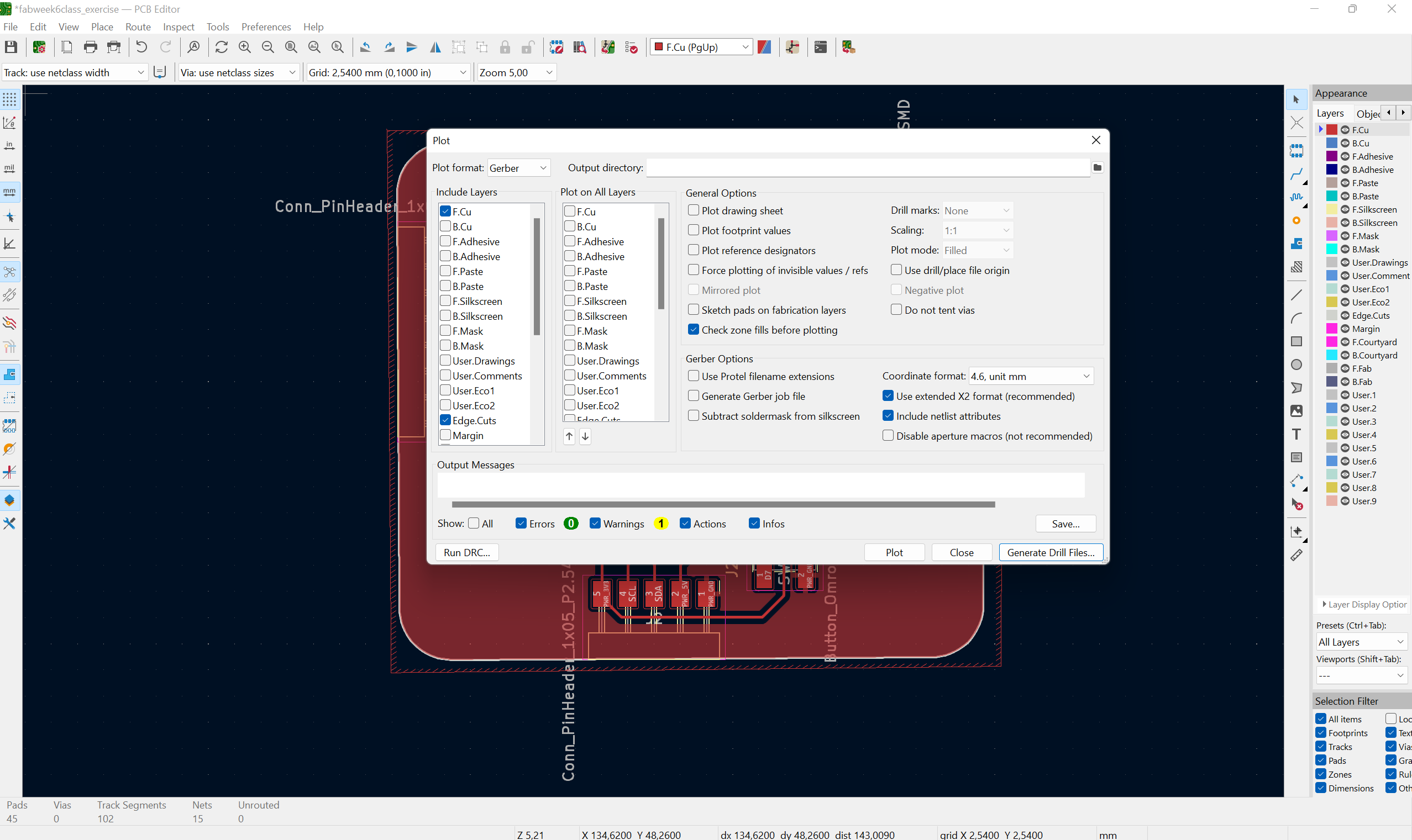
The PCB did not have any errors. Afterwards, I exported it to the Gerber X2 file which was used by the LPKF machine in the Fab Lab. The steps are: 1) File -> Plot (Figure 2). 2) Check the “F.Cu and Edge.Cuts” options, then Generate Drill Files. Map file format is Gerber X2 (Figure 3).
The corresponding design files (including Gerber X2 files) in Kicad can be found from here.
PCB manufacturing by LPKF machine
The following pictures (in sequential order) illustrate the steps I followed to mill the PCB Board on the LPKF machine.
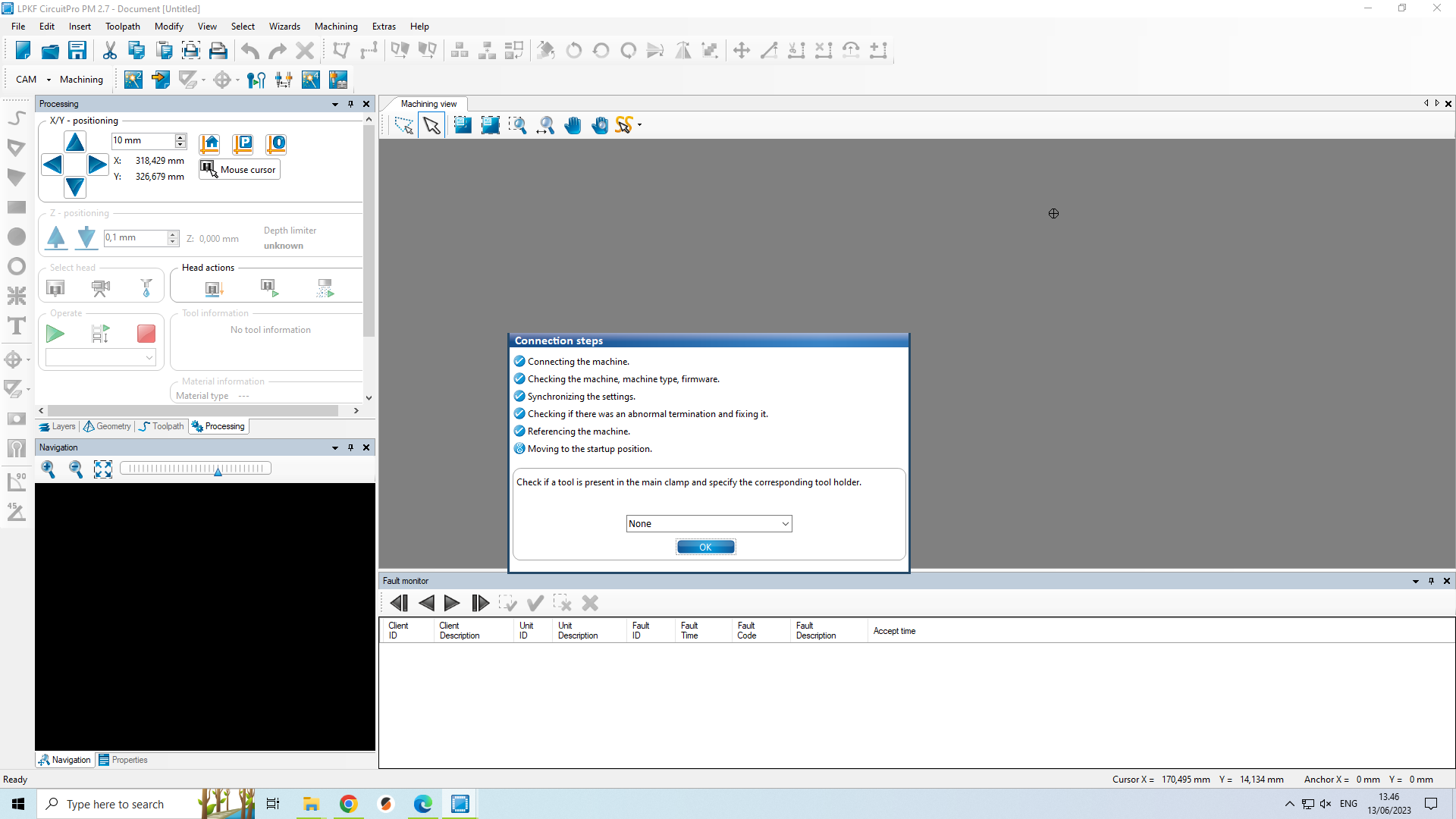 Fig 4: Circuitpro initiates a connection with the LPKF machine at the beginning when it is opened.
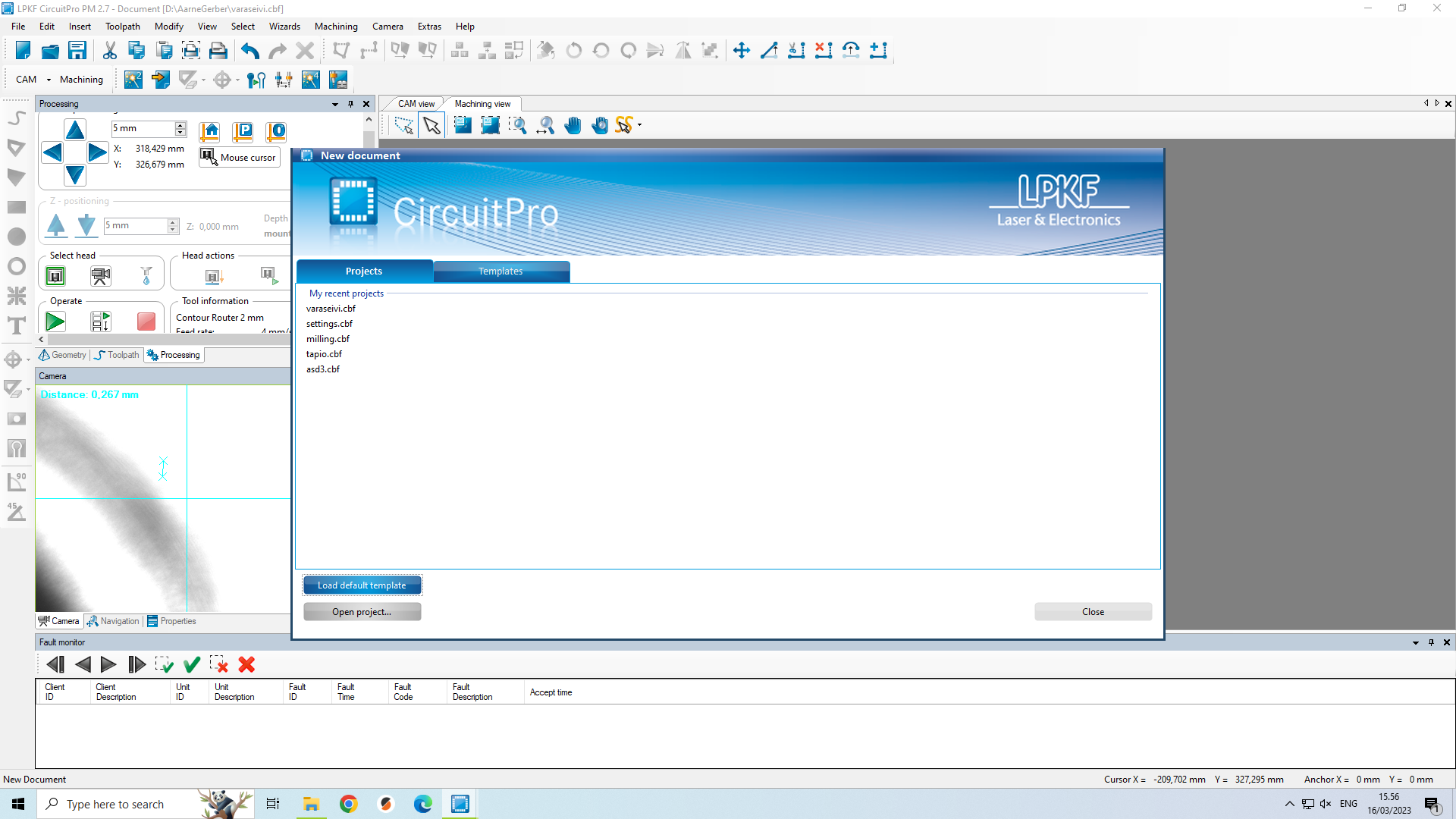
We choose “Load default template”. After this step, there are total 4 major steps:
-
Process planning wizard, where we have to select type of the process (Process PCBs, vs. Process 2.5D elements), the number of layers the board is going to have if Process PCB were selected in the beginning, and the kind of substrate we are going to use for milling the PCB Board.
-
Importing Gerber files, where we load the “Edge cuts” and “Front copper” .grbl files into the program.
-
Generating toolpath, where the actual toolpath for the milling is generated.
-
Board Production Wizard, where we mount the base material in the machine with the help of adhesive tape, set the area on the base material (by deciding P1, for the lower left corner and P2 for the upper right corner) within which the board will be milled with the toolpath generated in step 3, and then the actual milling begins. At the beginning of the milling, we also need to calibrate the width of the cut by milling a line (more details on this below).
Loading Gerber file and adjusting initial settings in the Circuitpro program
Process planning wizard
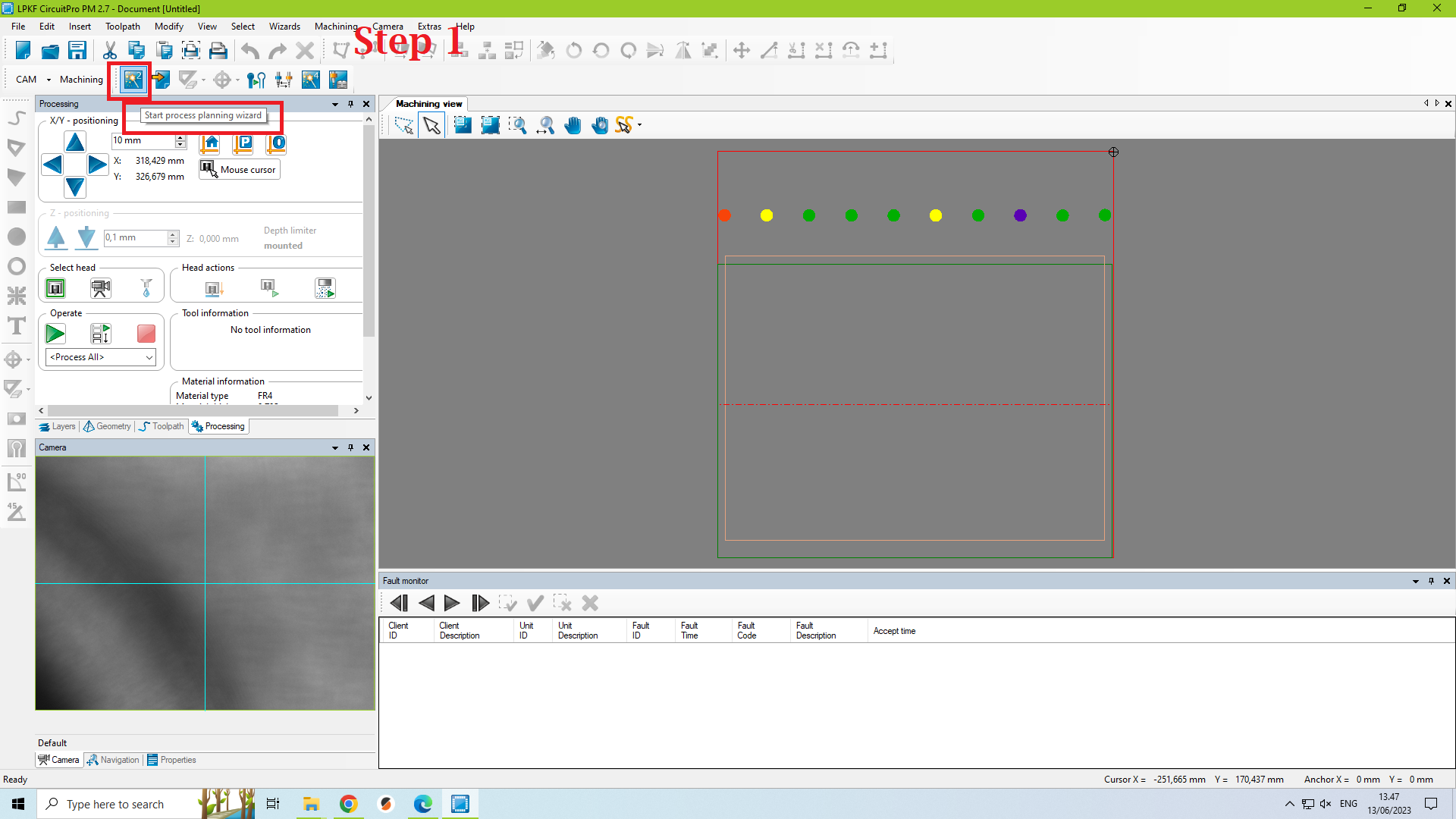 Fig 6: The Tab highlighted in red shows a button to start the Process planning wizard. Click on it to start the process.
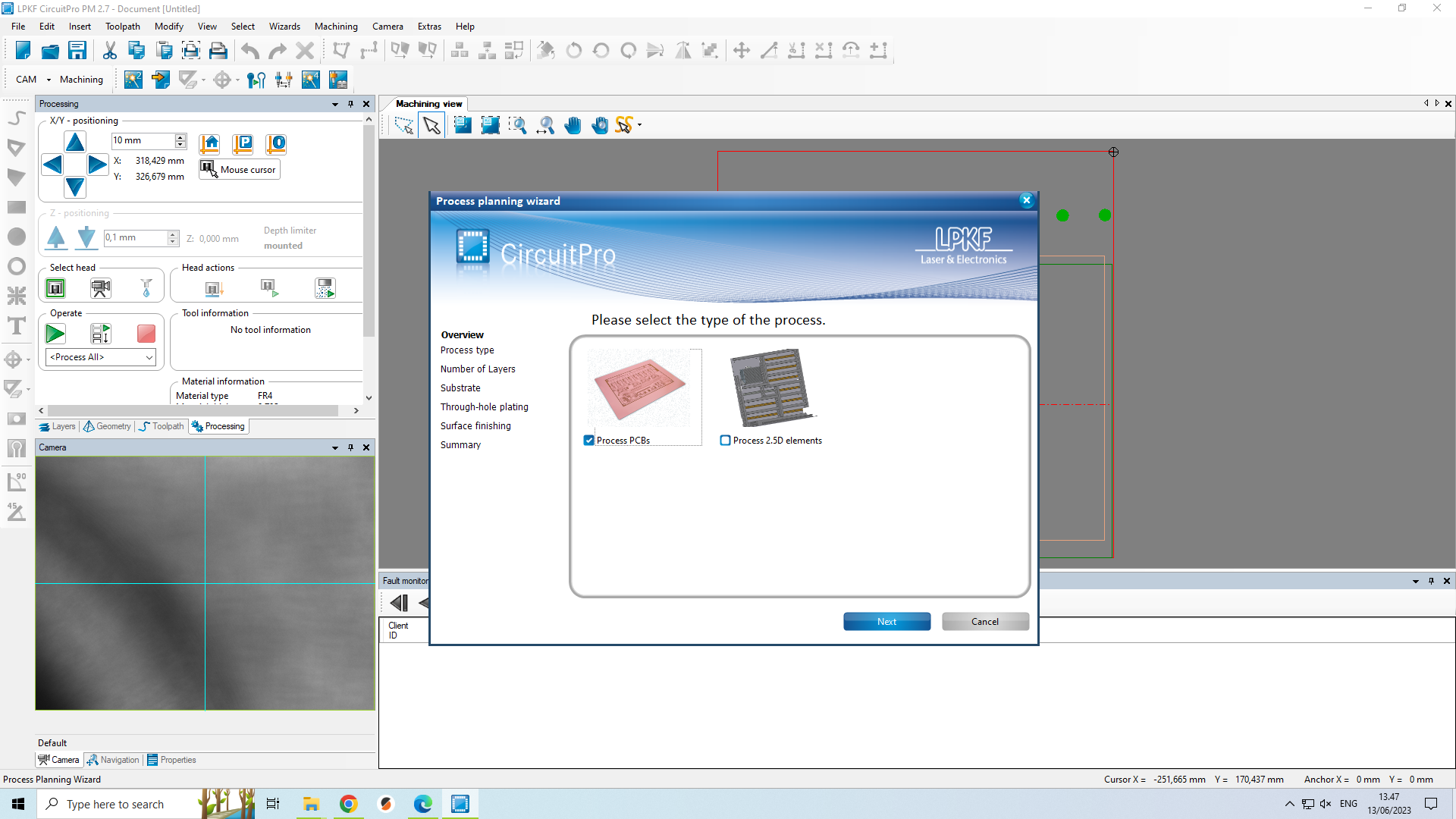 Fig 7: Next we need to choose the type of the process. I chose Process PCBs and then clicked Next.
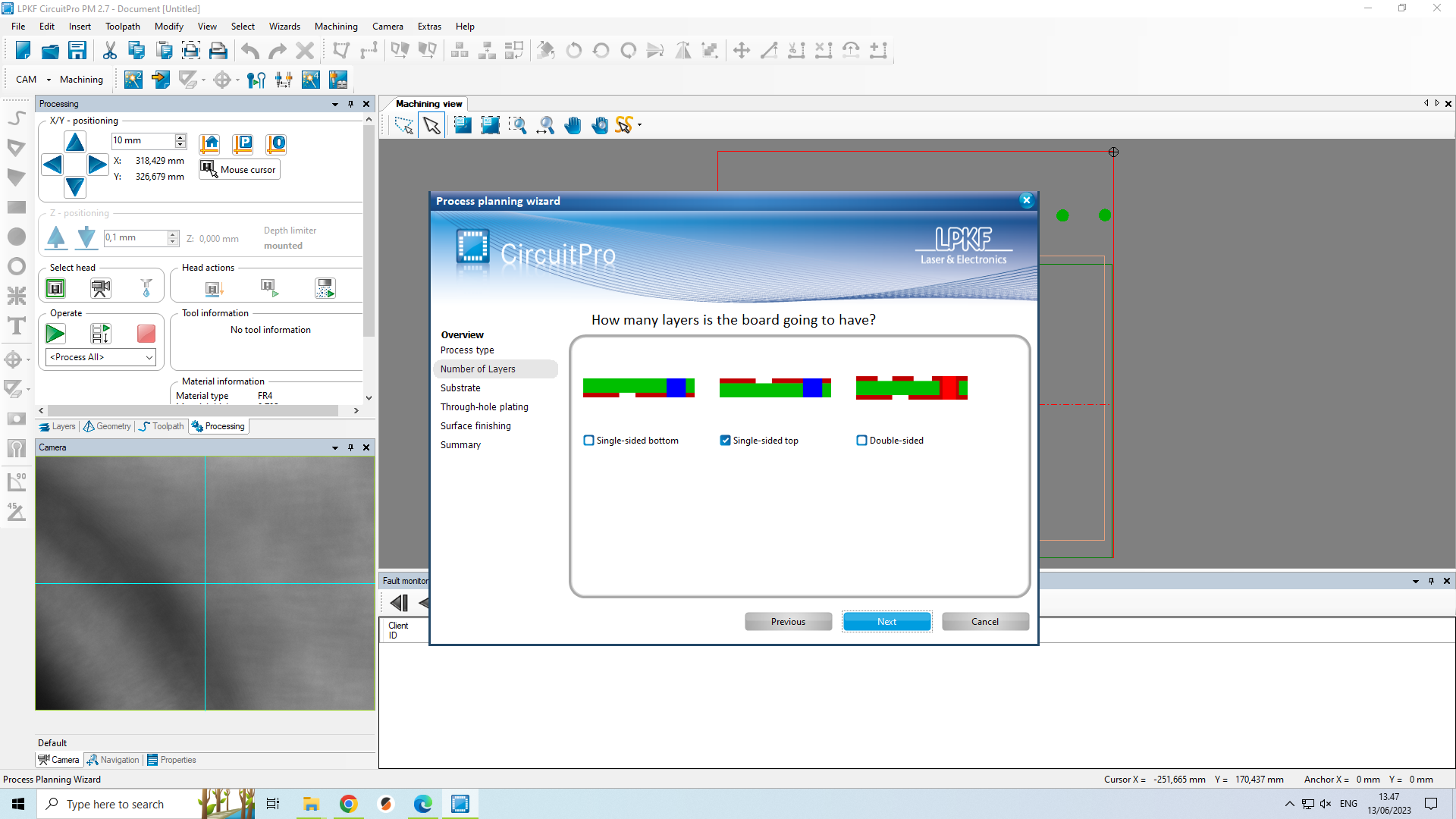 Fig 8: Once Process PCBs have been selected in the previous step, next we need to mention the number of layers the PCB is going to have. I chose a Single-sided top and then clicked Next.
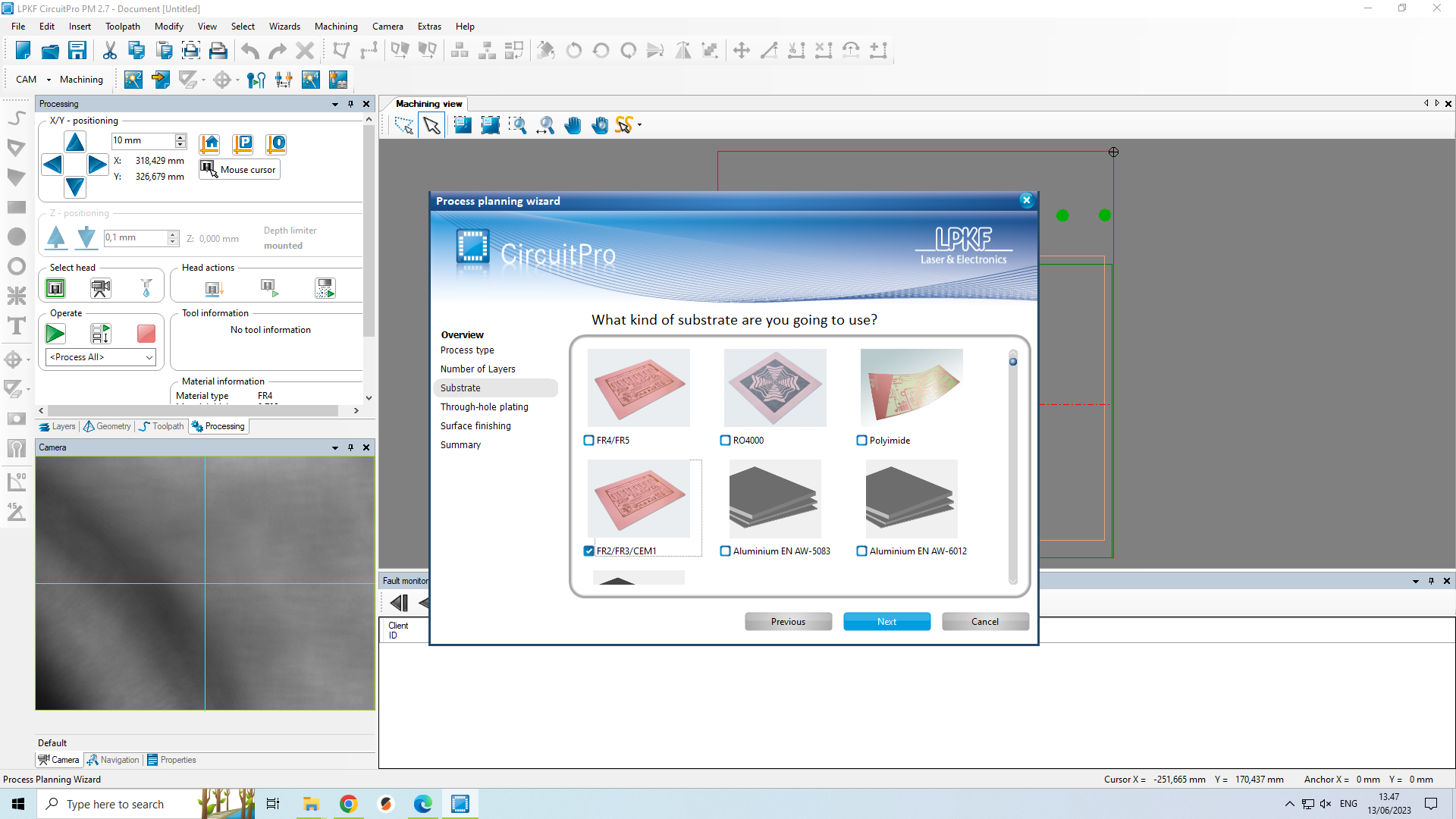 Fig 9: Next we need to choose the type of base material/substrate on which the PCB will be milled. I chose FR2 since our substrate in the lab was of this type. Then, Clicked Next.
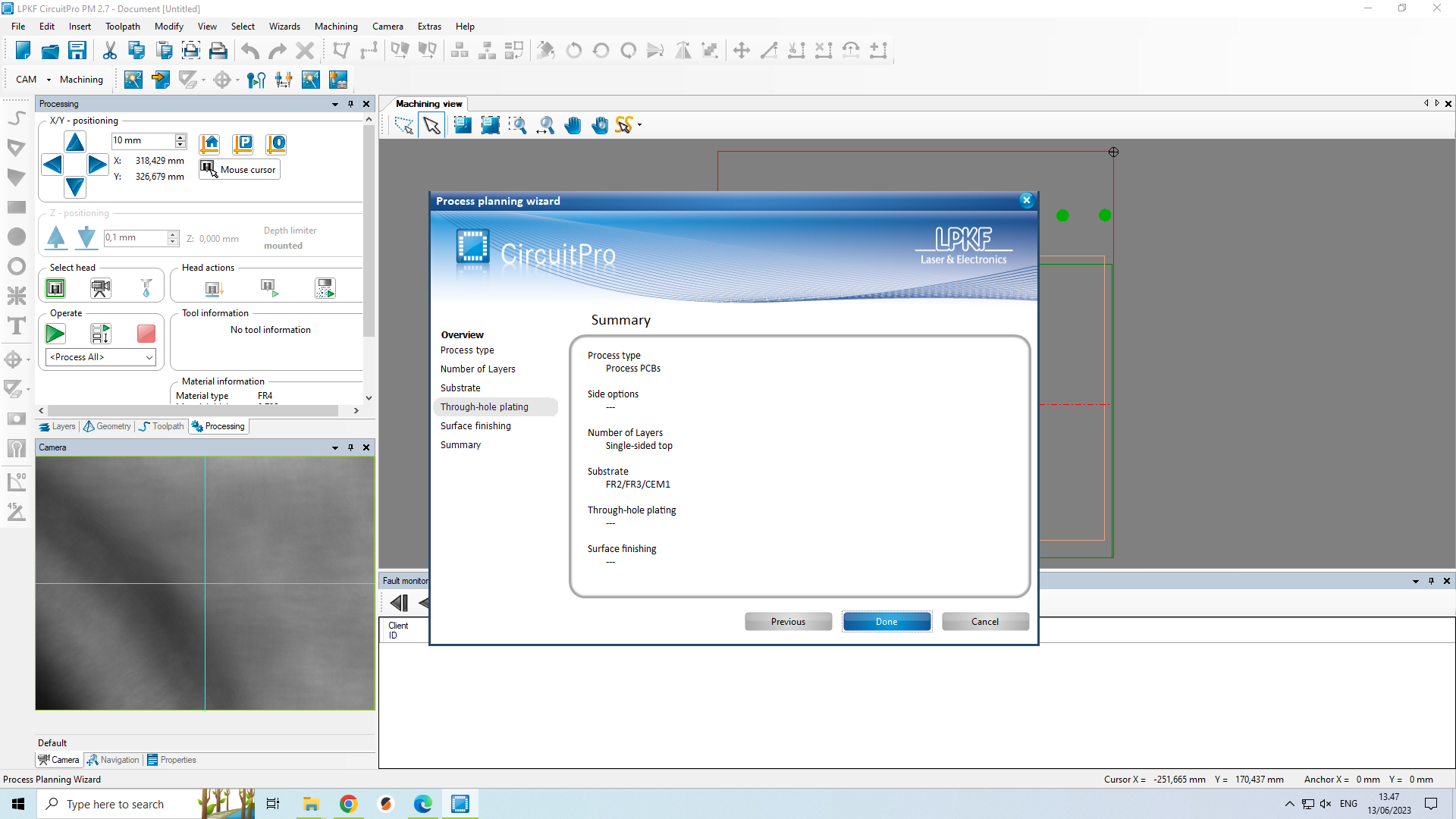 Fig 10: This dialogue box is the end of the process planning wizard and is showing all the settings we chose for process planning. If all the settings are correct, then click Done. If not, then Click Previous to go to the previous steps to modify the setting.
Importing files
Figures 11-14 show the process of importing the following two Gerber files (previously exported from KiCad), and visualizing them.
- “Edge cuts” .grbl file
- “Front copper” .grbl file
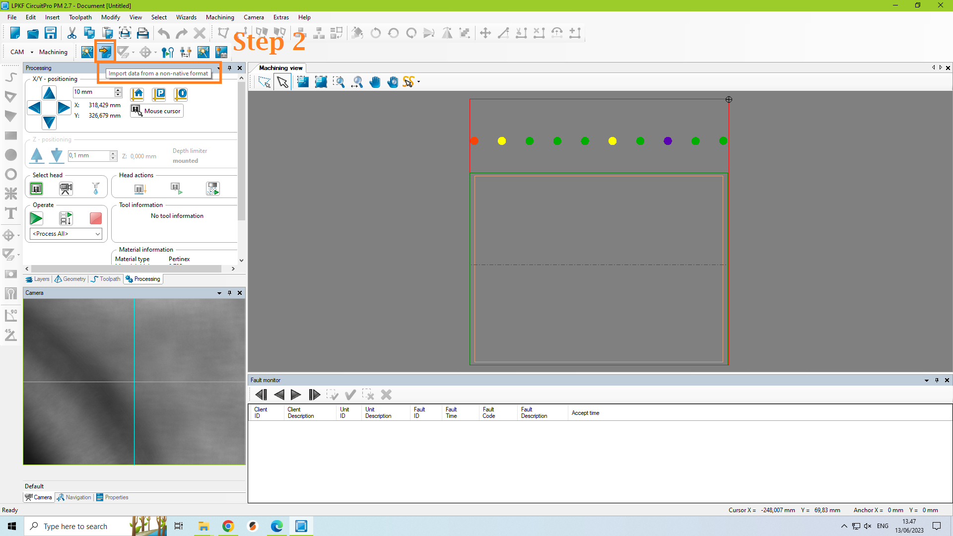 Fig 11: Import menu for loading Gerber files for milling.
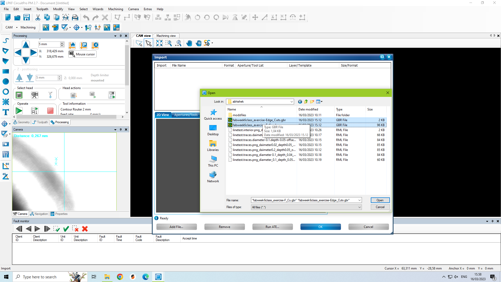 Fig 12: Importing Gerber files.
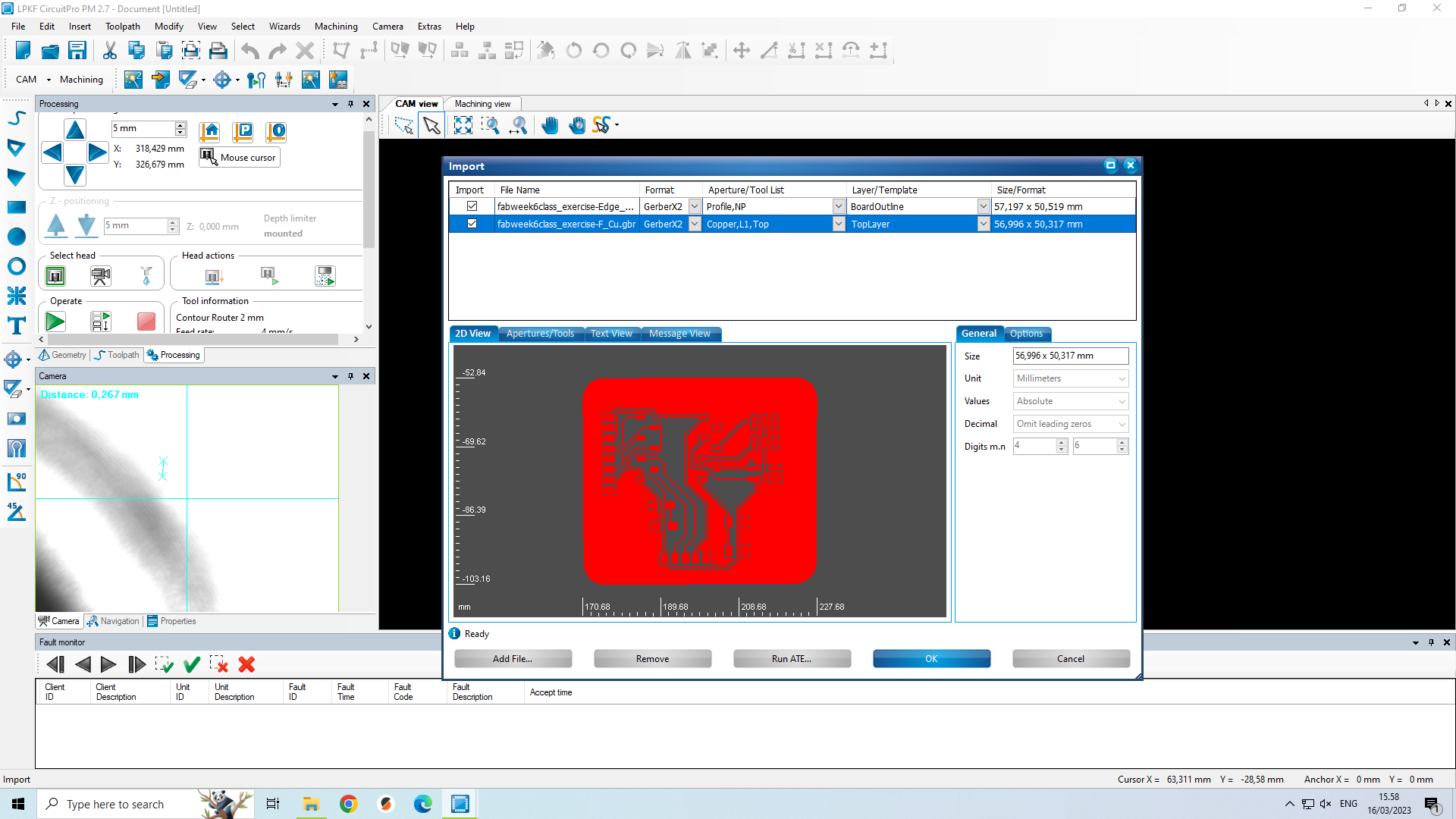 Fig 13: Visualization of PCB’s Copper region Layout after importing Gerber file into CircuitPro Software.
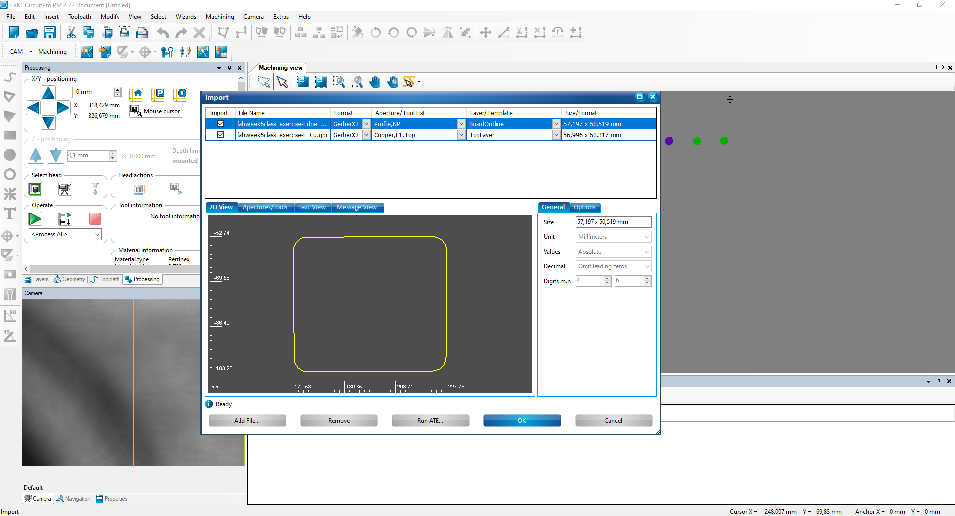 Fig 14: Visualization of PCB’s Edges after importing Gerber file into CircuitPro Software.
Figure 15 shows the milling path after exporting the “Edge cuts” and “Front copper” .grbl files into the Circuitpro program.
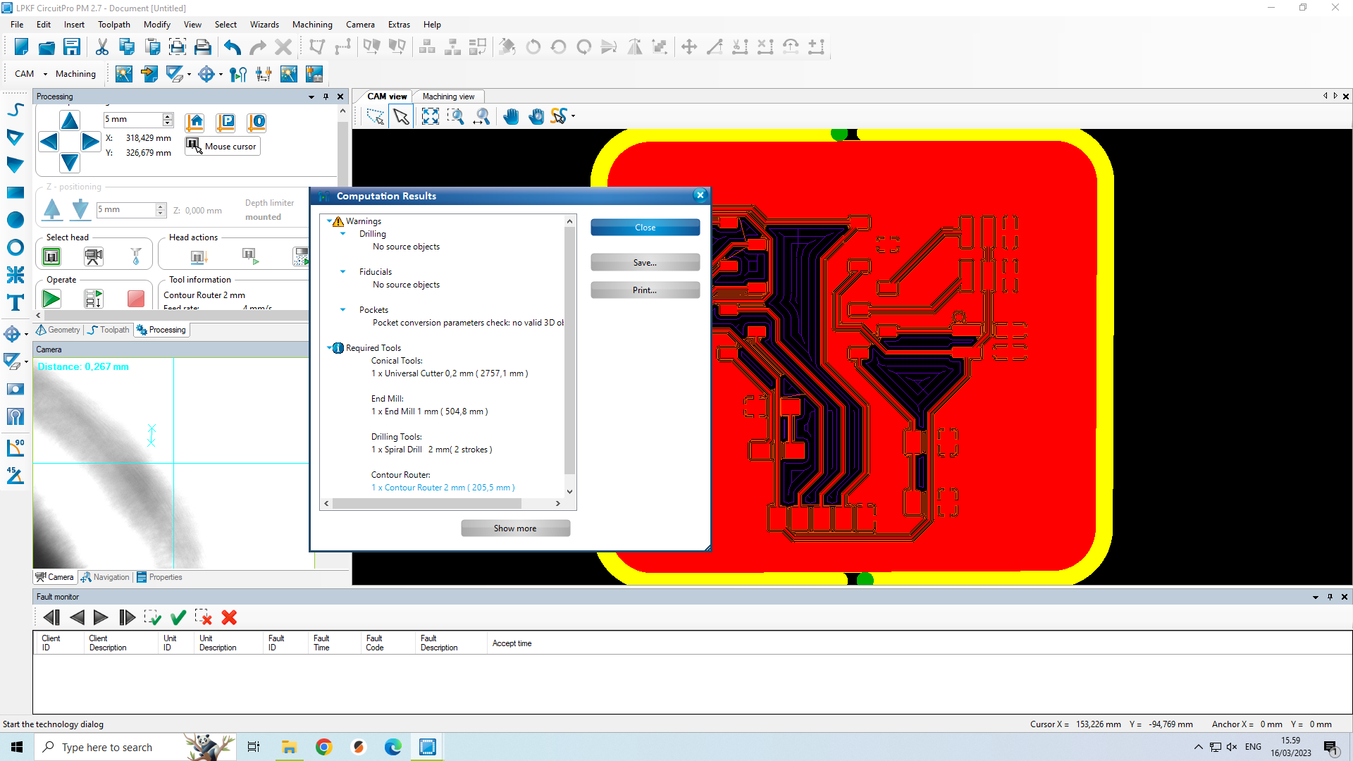 Fig 15: Milling paths.
Generating toolpath
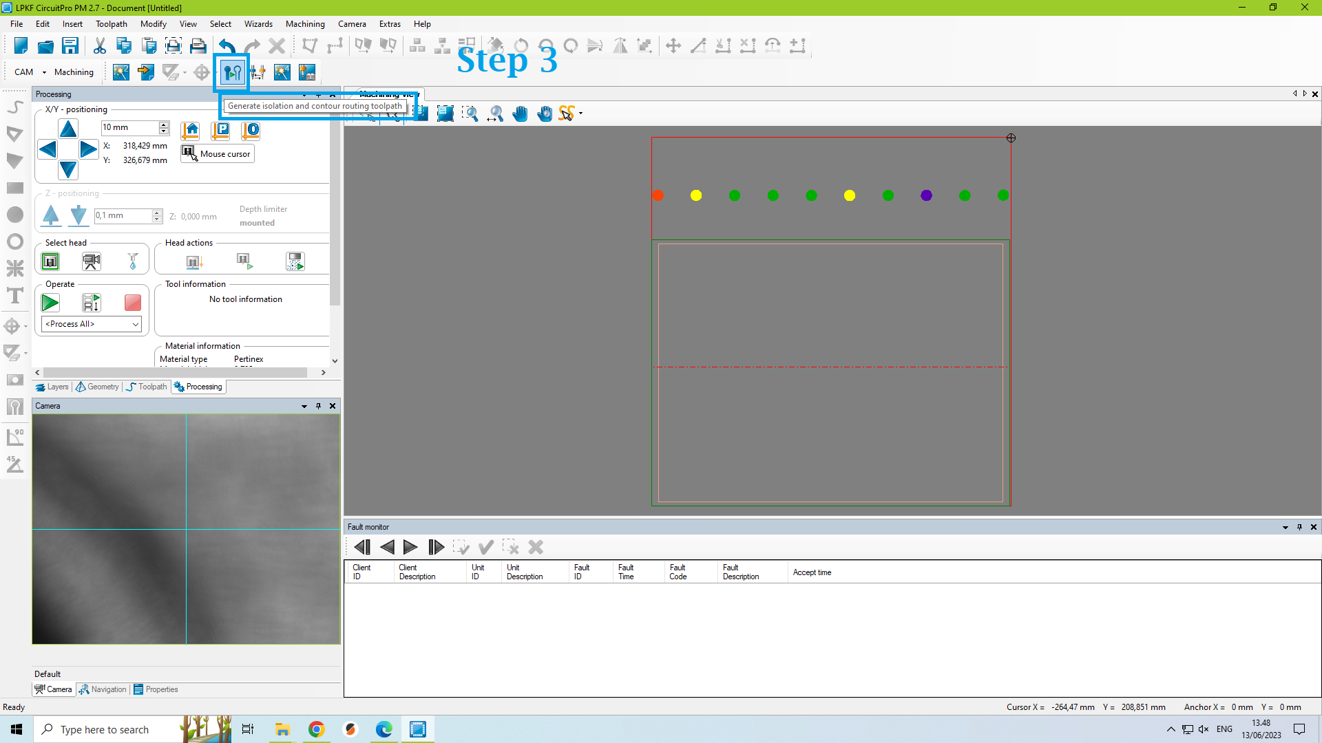 Fig 16: The Tab highlighted in blue color shows the button to generate isolation and contour routing toolpath. Click on it to start the process.
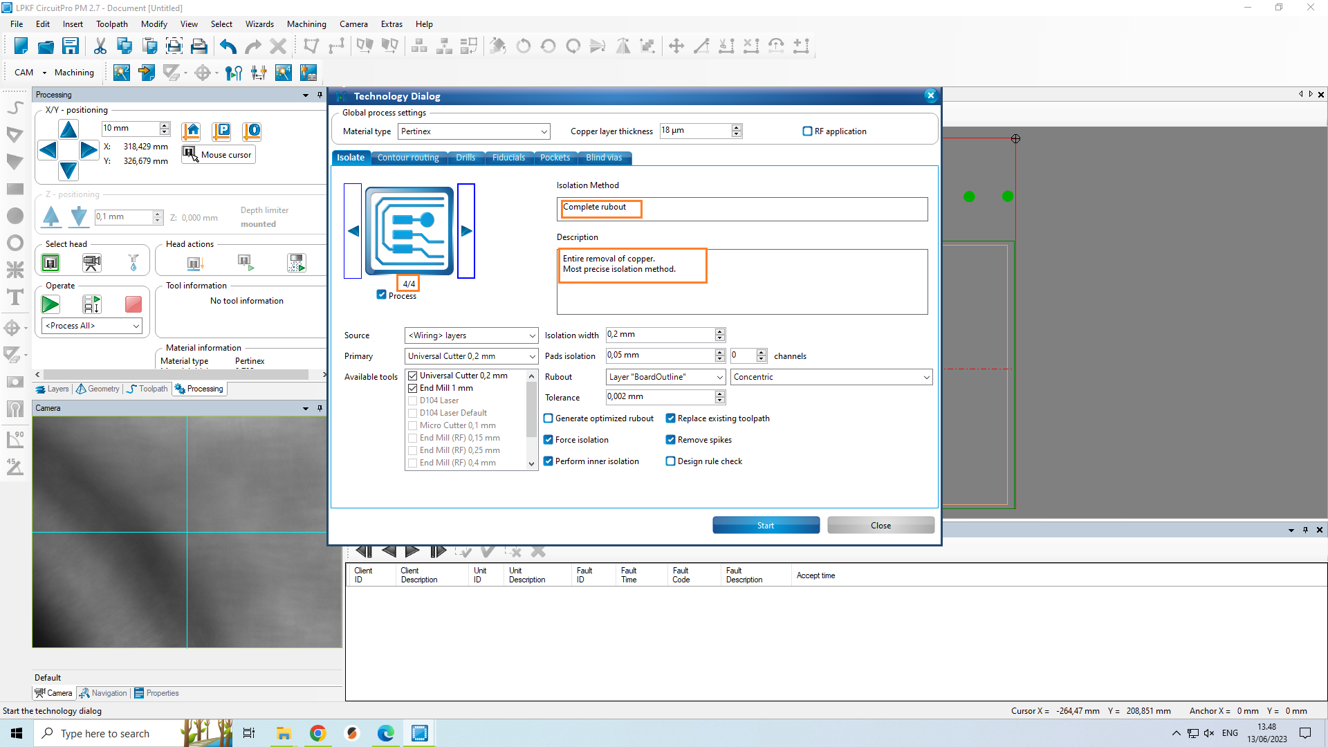 Fig 17: Select appropriate Isolation routing. I chose the one shown in the image.
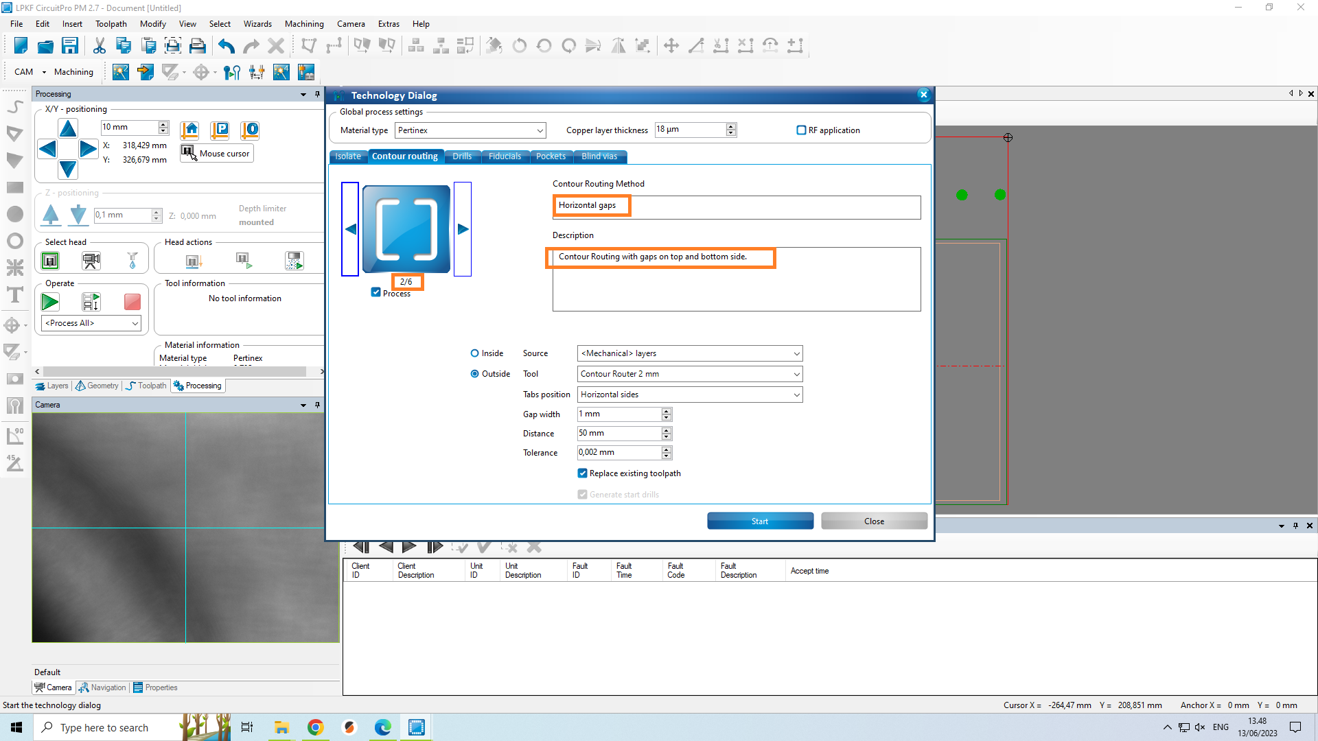 Fig 18: Select appropriate contour routing. I chose the one shown in the image. Then, select Next
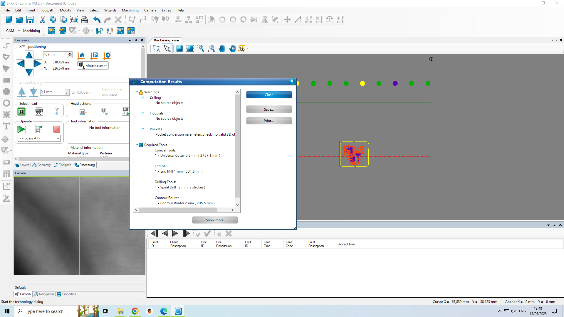 Fig 19: The dialogue box shows computational results and our settings. Click Close or Save.
Editing contents of the tool magazine.
I call this step 3.5 because we need not make any modifications for the most part. Accepting the default setting will do the job just fine.
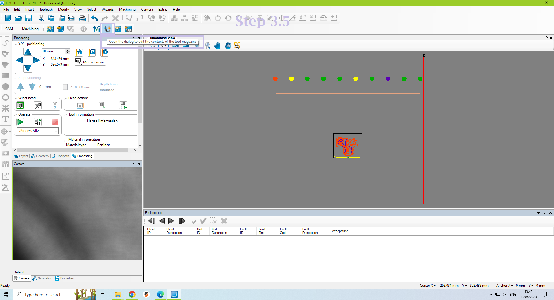 Fig 20: The Tab highlighted in the coloured rectangle shows the button to edit the contents of the tool magazine.
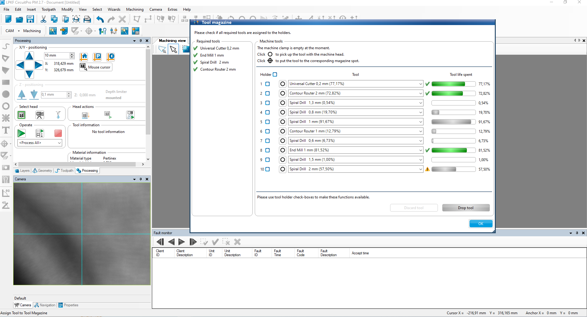 Fig 21: Showing options of the tool magazine content.
Board production wizard
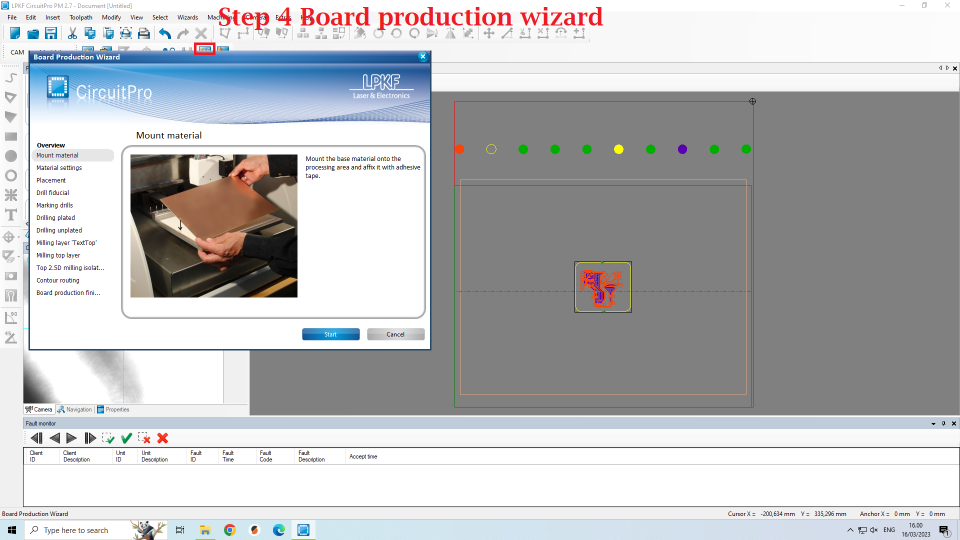 Fig 22: The Tab highlighted in deep red shows the button to start the Board production wizard. From here, the actual production of the PCB starts. The tab is slightly hidden because I had already clicked the button which generated the dialogoue box which hid it.
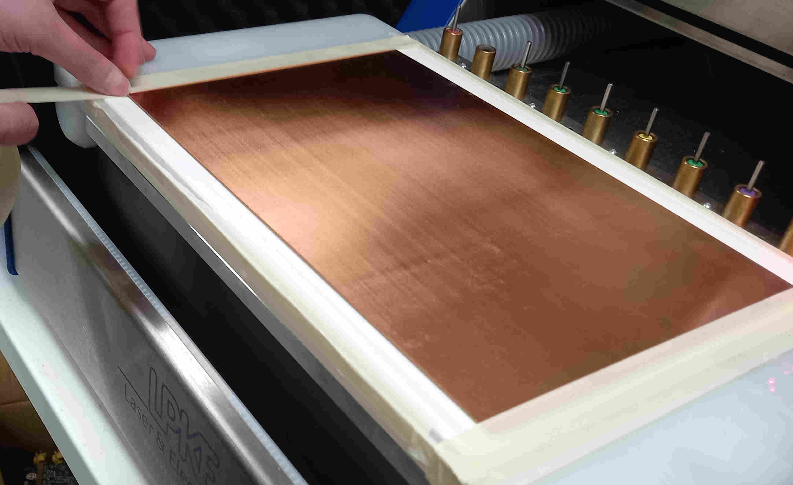 Fig 23: Next we mount the FR2 substrate inside the milling machine with adhesive tape.
Next, we need to select the region within which milling will be done to make the PCB. P1 refers to deciding the lower bottom corner.
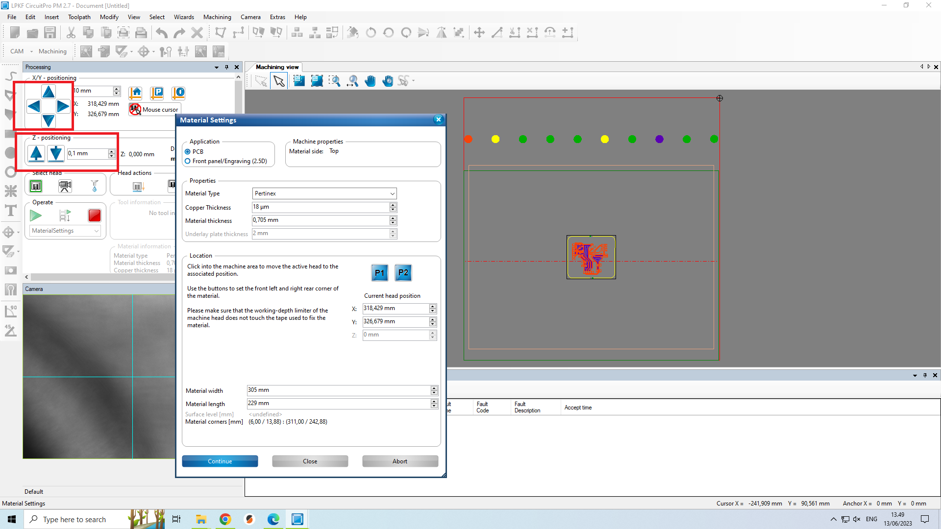 Fig 24: We use the allows highlighted in the red colour rectangle to locate the lower bottom corner of the milling region.
Next P2 refers to deciding the upper right corner of the region within which the milling will be done.
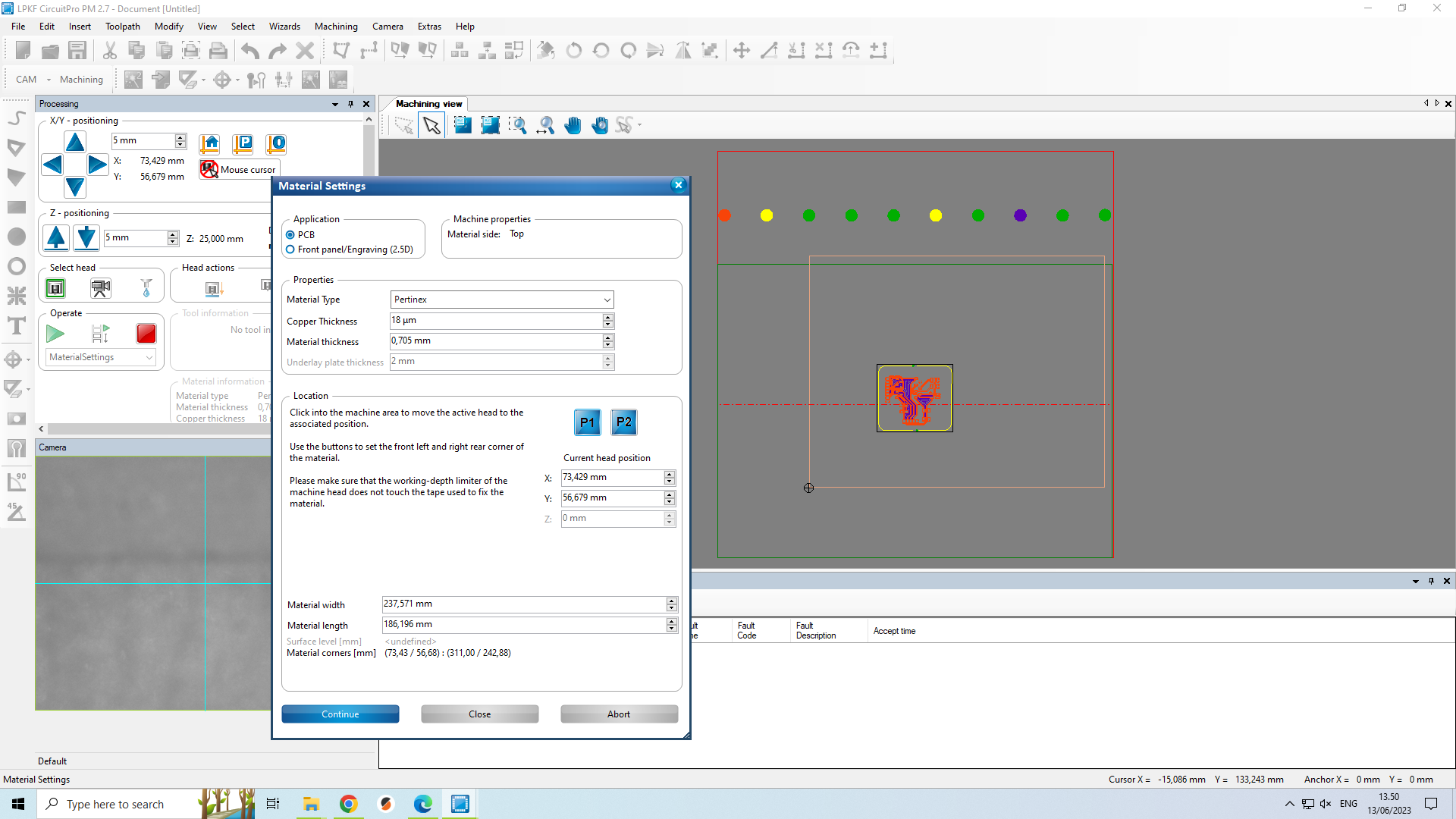 Fig 25: Next we click any region in the upper right region. The safe estimate is to place P2 at the farthest top and the farthest right corner from P1 which is still within the area of the mounting material. Once we locate such a point, we click on it. Then click P2. It will create a boundary within which our milling should be done. Then, click Continue.
 Fig 26: We can move the board layout within the created boundary for milling in the previous step.
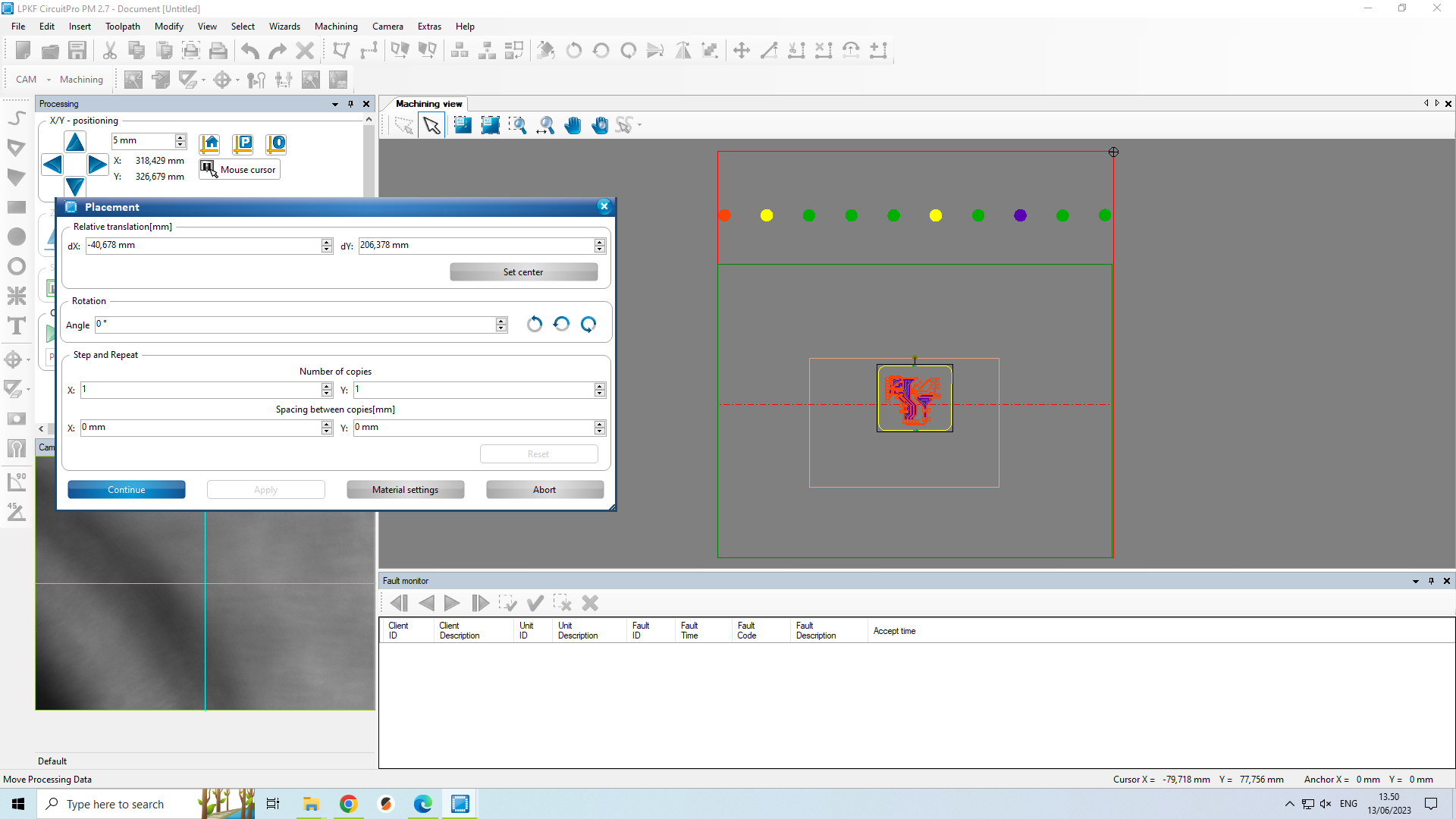 Fig 27: After moving the board to the boundary region, select Continue in the Placement dialogue box. After this milling begins.
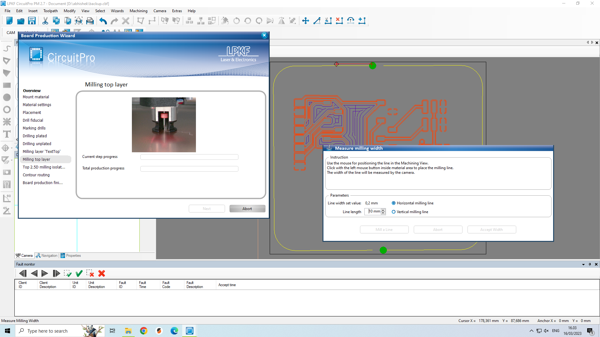
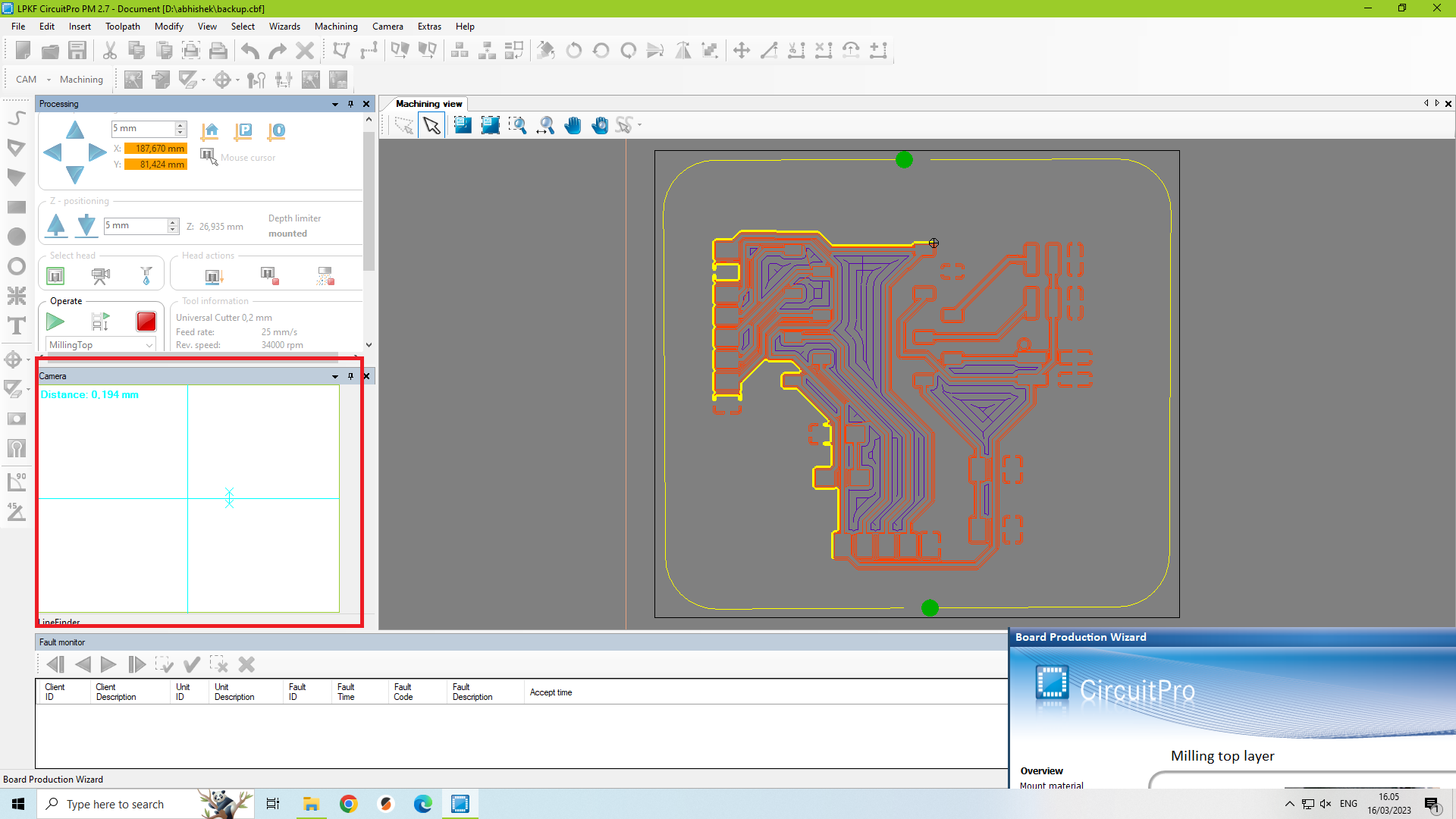
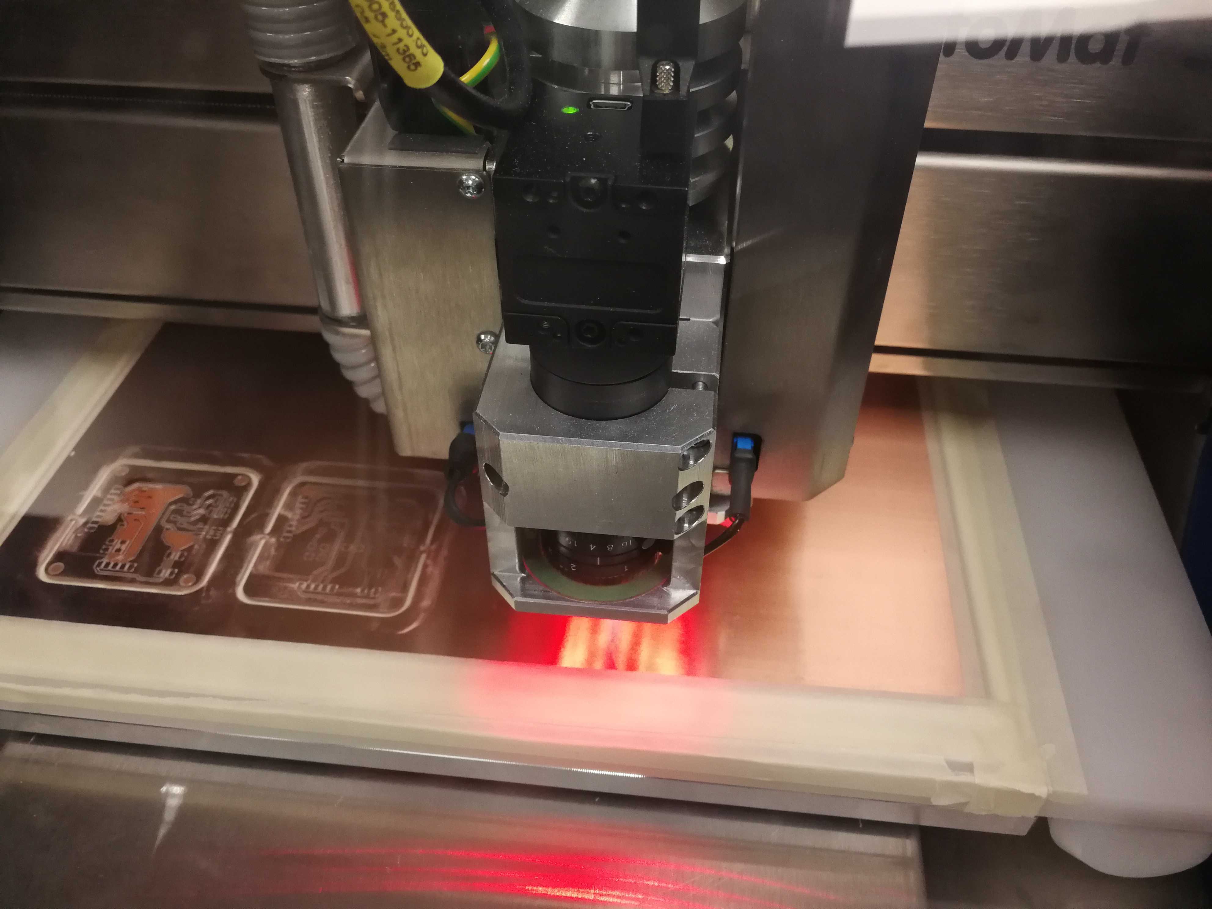
Immediately it asks to set the drilling width. For horizontal milling line, we click a region outside the board layout and then mill a line, and we accept the milling width. Usually accepting the default width does the job just fine. Then, it comes the length of the vertical milling line. For that. we look at the camera region (shown in red rectangle in Figure 29). If the auto-focus is correct, then we right-click, choose “Point to Point” measure mode, and pick two points vertically within the focus region. In the Figure 28, it shows the height to be 0.194mm, then we accept the settings. It begins the drilling.
Milling in Progress
Actual drilling begins.
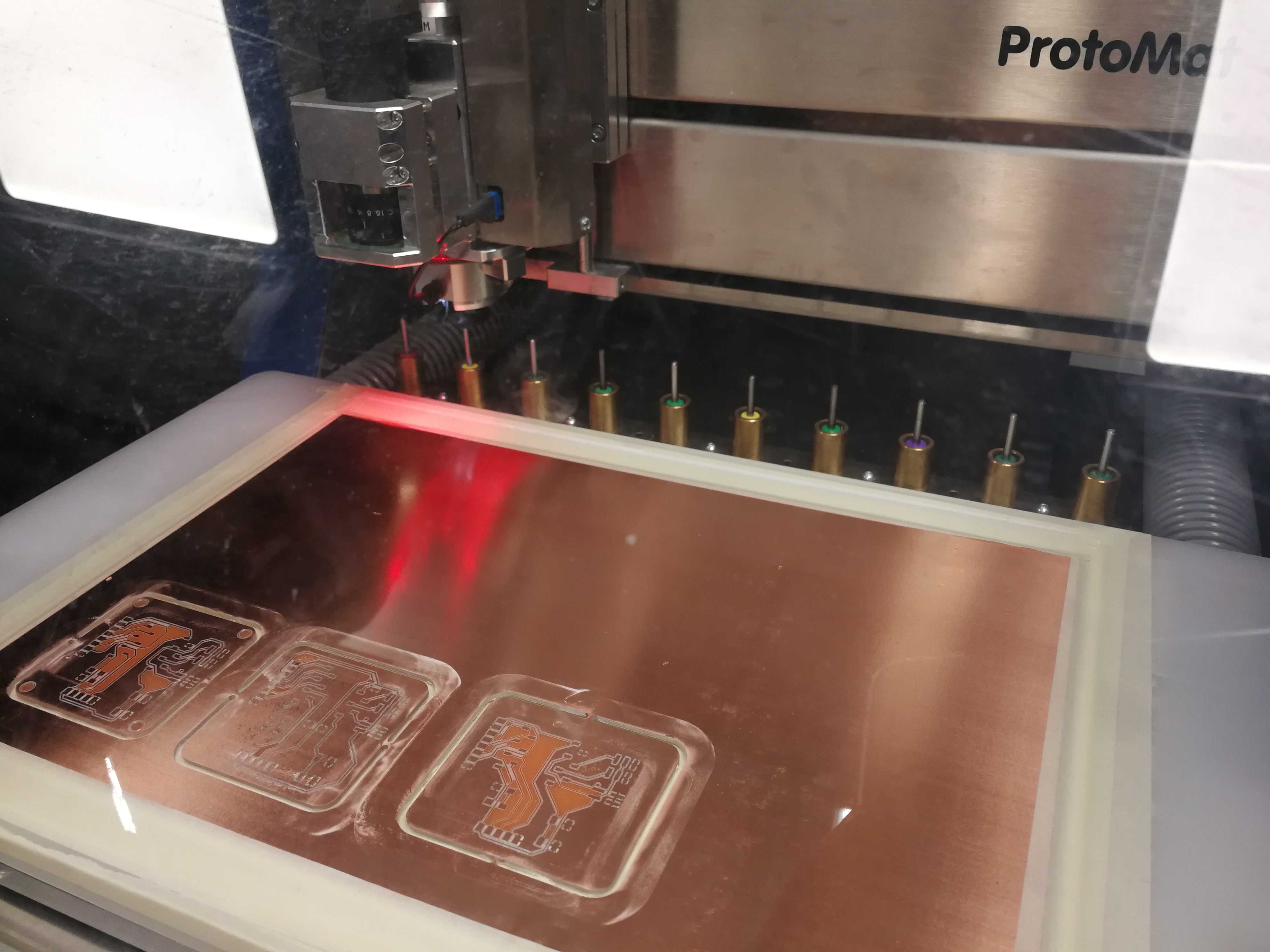
Milled PCB Board
PCB Soldering
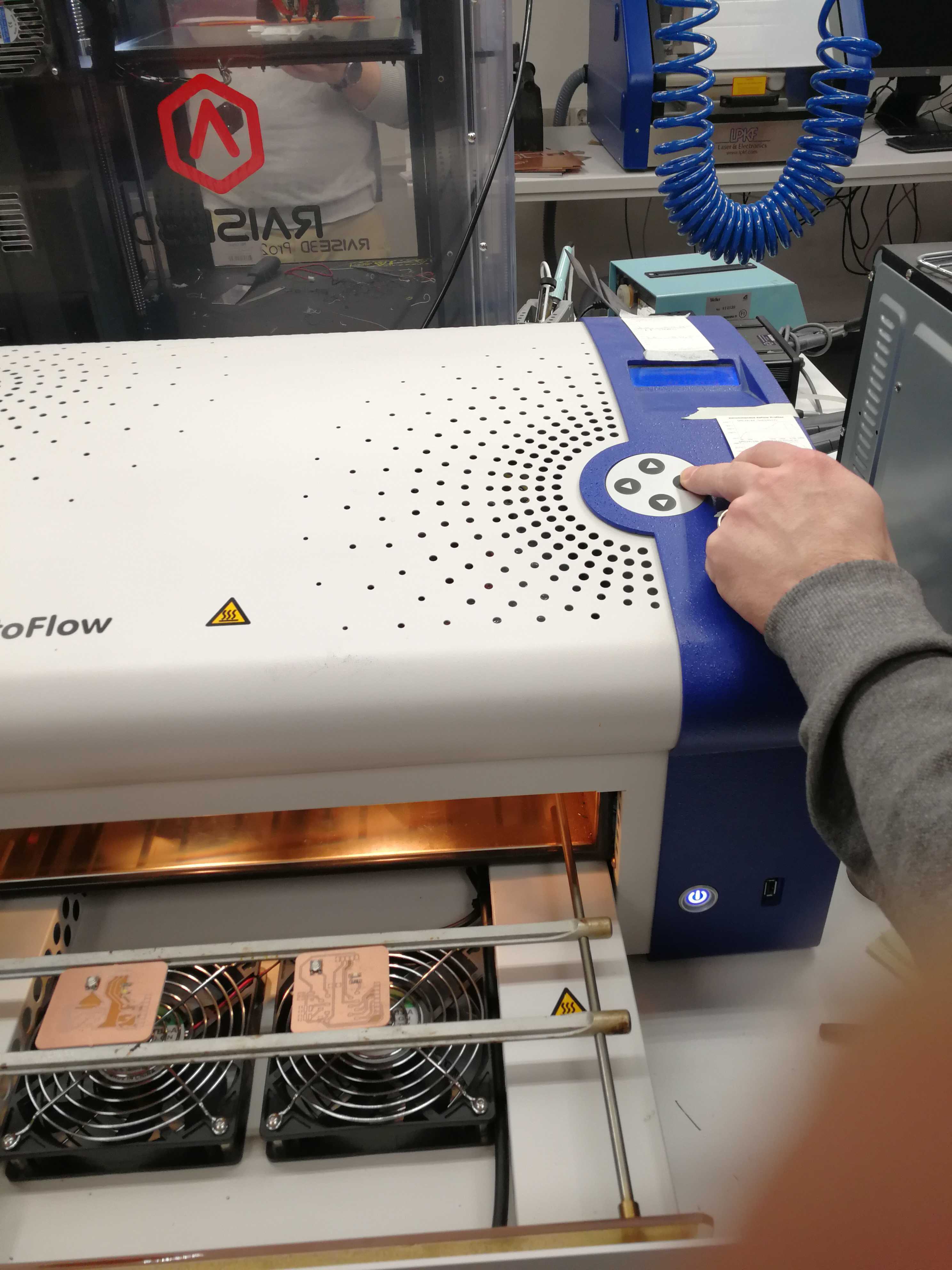
After milling the board, I soldered the board in two phases: 1) Solder paste and Reflow Oven 2) Manual soldering
Soldering with Solder paste and Reflow Oven
During the first phase, solder paste was applied to the board so that the led, button and resistor could be later soldered in Reflow Oven (Figure 32).
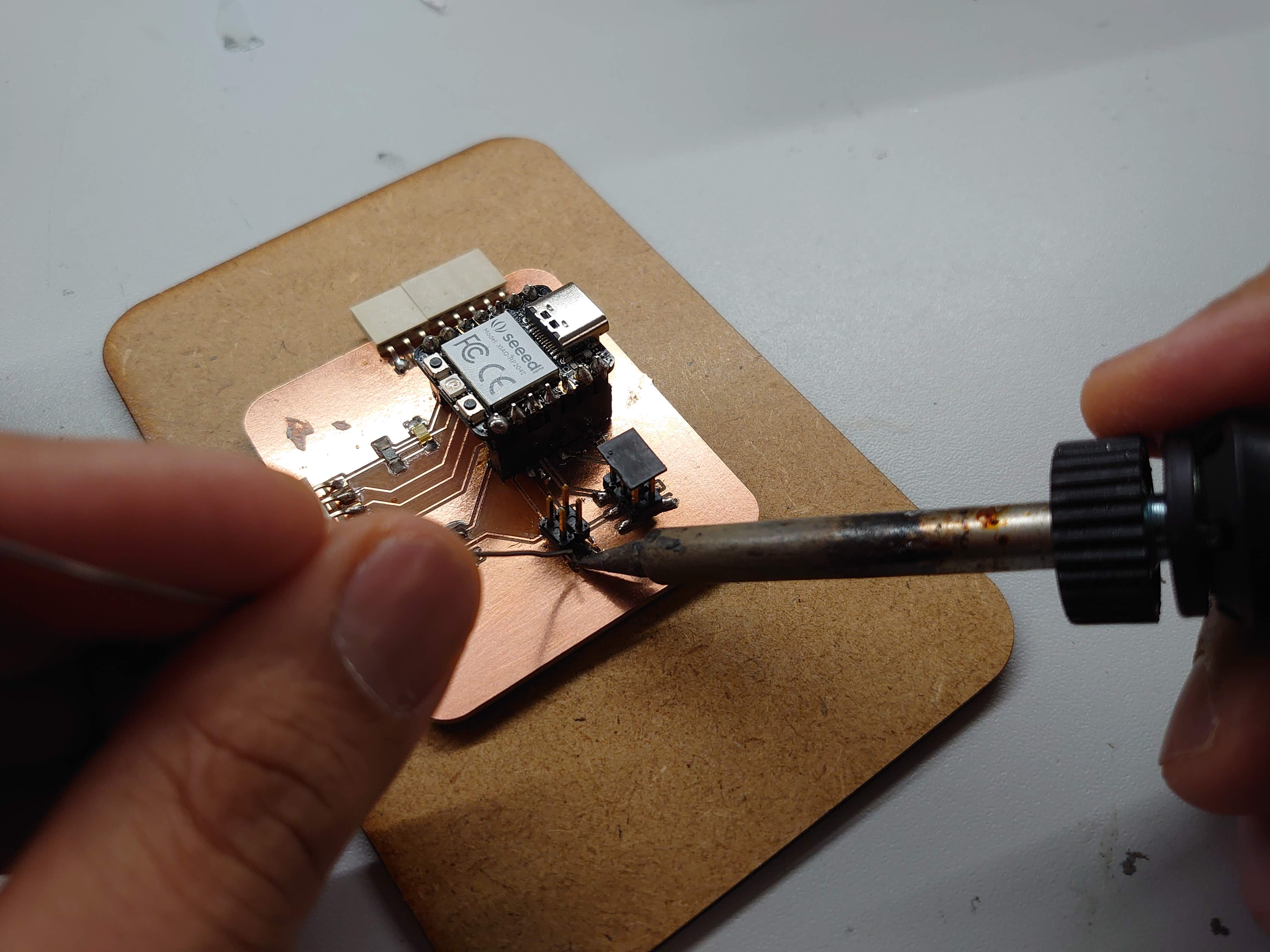
Manual soldering
Afterwards, I soldered the remaining components manually by hand soldering (Figure 33).
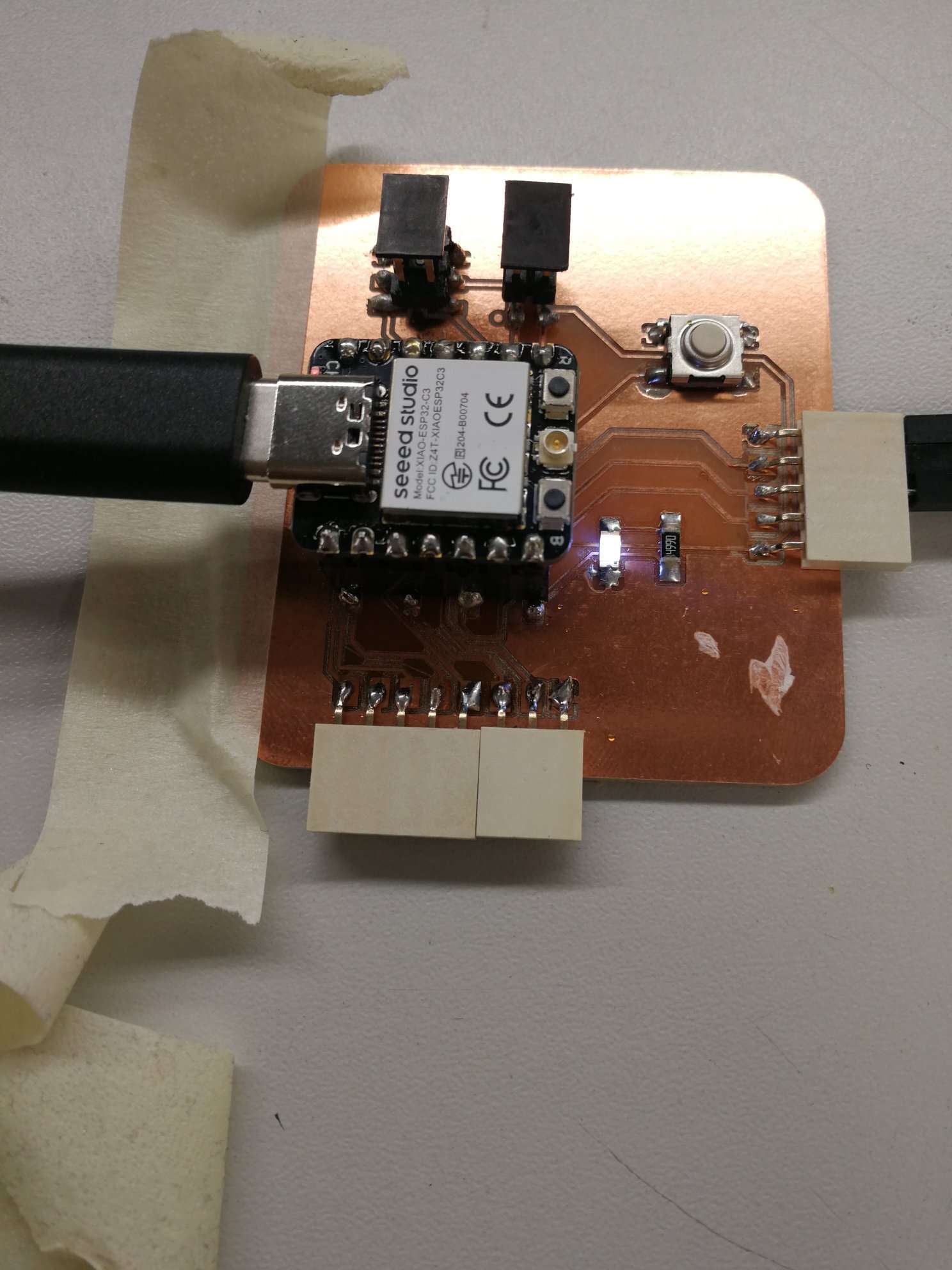
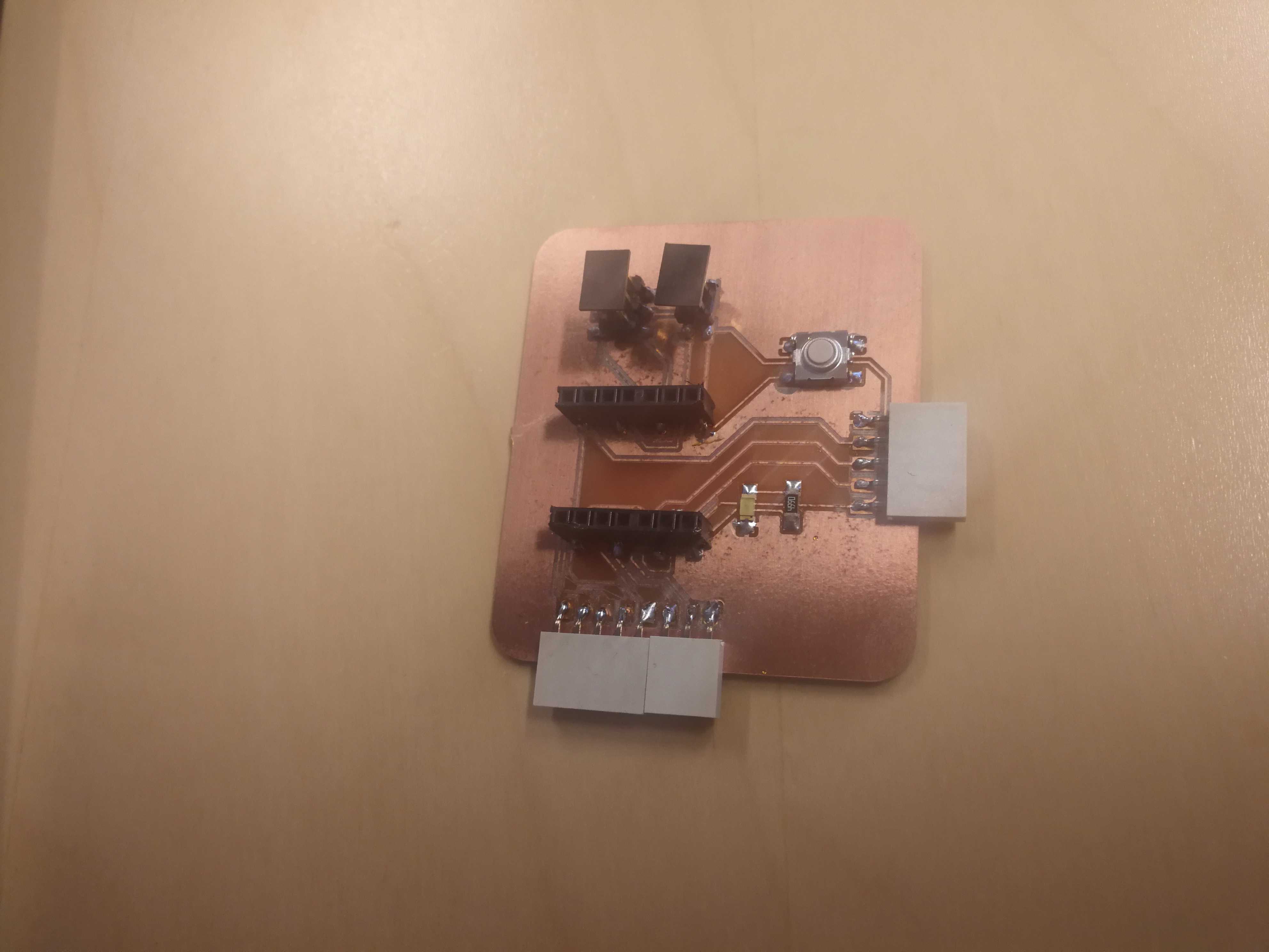
Final PCB
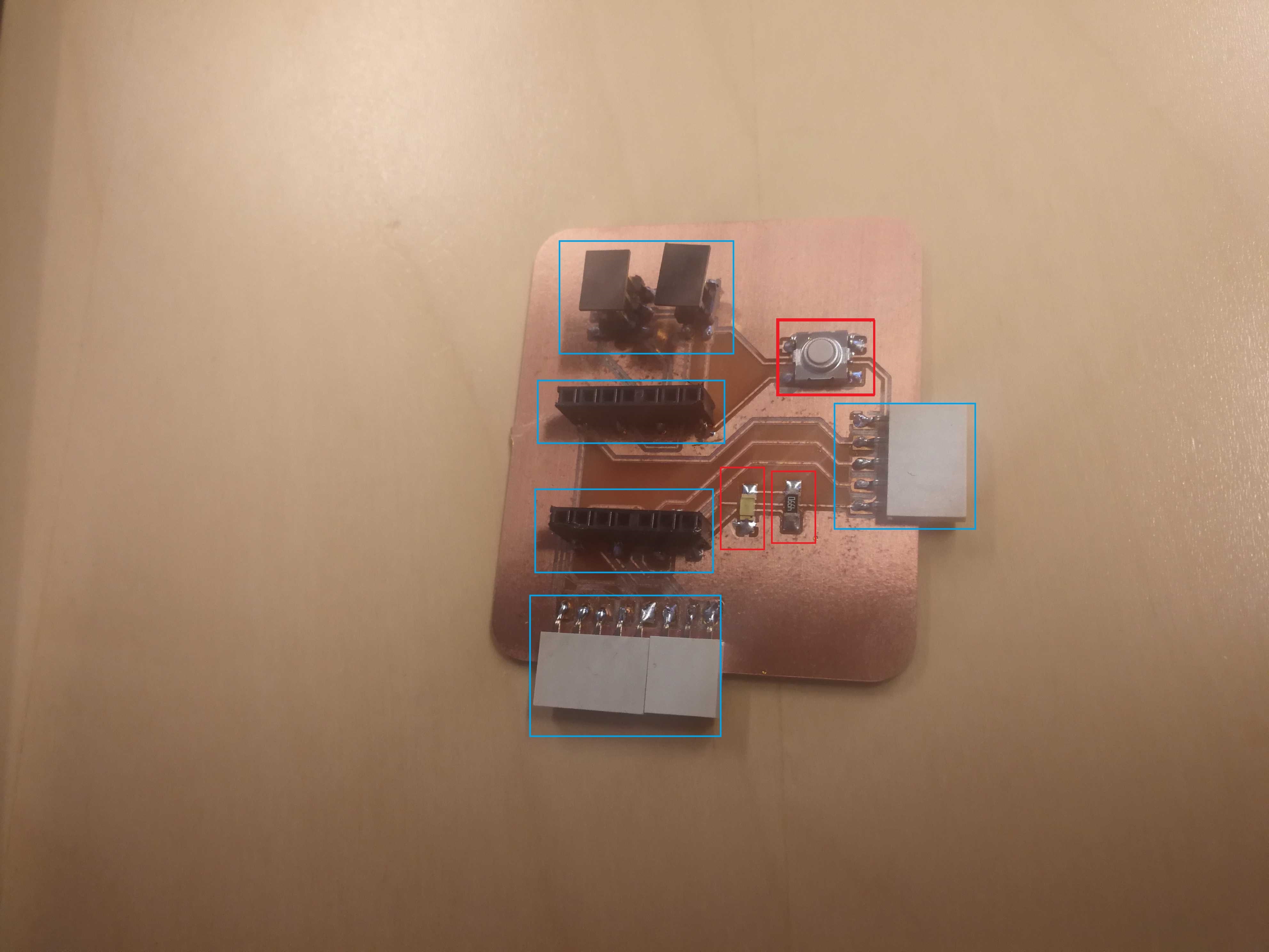
The final PCB looked like the following:
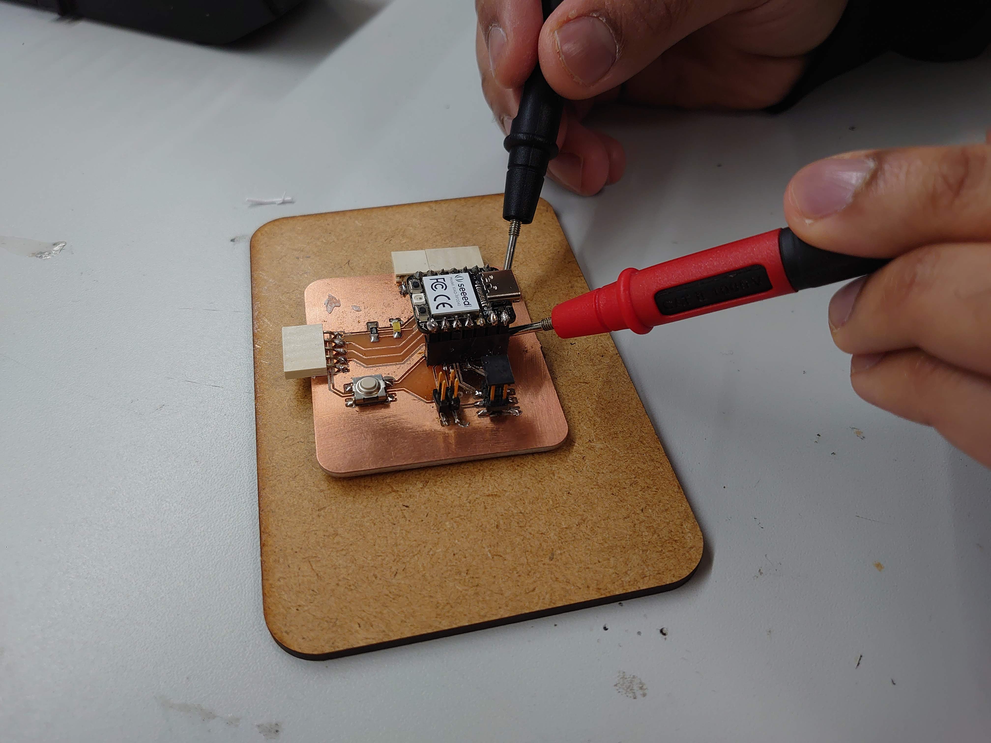
Note on Soldering: I had a lot of issues during the soldering process: either I put too much solder which led to short-circuiting, or I put too little solder which led to a very weak attachment of connector pins with the copper on the board because of MCU Xiao RP2040 got detached with the connector many times when I tried to remove from the board. The connector should have remained attached to the board. But eventually, I got it working. I tested for short-circuiting with the multimeter available in the Fab lab (Figure 36), then did some further testing mentioned in next the section.
Testing the board: Blinking the LED by setting HIGH on MCU Pin D6
Figure 37 shows the outcome of one snapshot of the blinking experiment done in Week 4. Embedded Programming. I further tested the manufactured PCB board in the output week with NeoPixel LED strip.