6. Electronics Design
This week I worked on getting my hands on electronics design with the help of KiCad doftware. It was the first time for me to work on building a custom printed circuit board. During the group work, I learned how to measure/test microcontroller power usage with a multimeter.
Setting up KiCad on the Local Computer
I followed the instructions mentioned on Fab Electronics Library for KiCad (in Readme.md file) to download and configure the required library.
Designing PCB schematics in KiCad
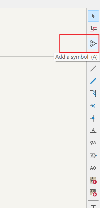
All necessary symbols for the circuit board were added by choosing “Add a Symbol” menu on the right hand side of the Kicad Window.
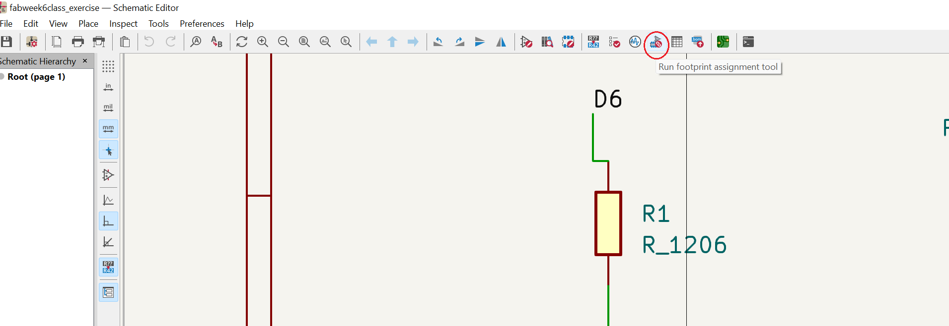
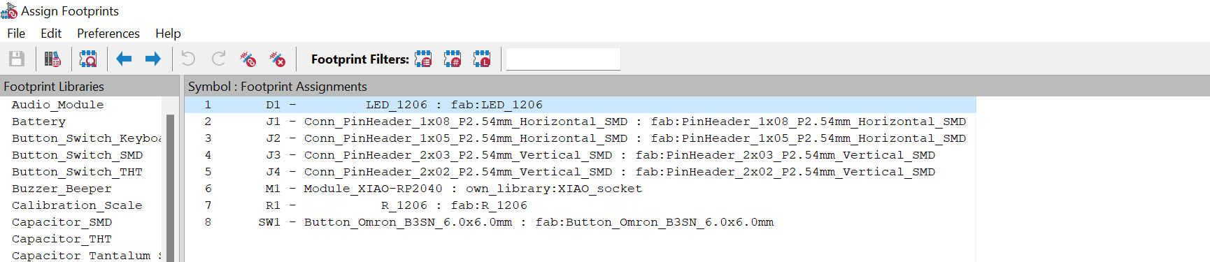
Footprints of the components was set so that they take optimal space on the board by choosing tools from upper menu as shown in Figure 2, then they were assigned as shown in Figure 3.
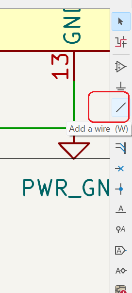
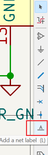
Wires and labels were added by choosing menu icons in Figure 4 and 5.
Each pins of components was connected with a wire (Shown as Green coloured strip connected to pins in Figure 6). Symbol PWR_FLG were connected to Ground and Power pins.
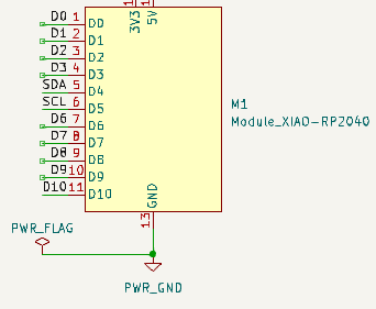
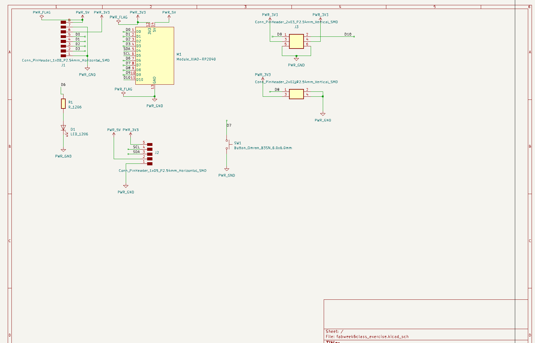
Figure 7 shows the complete and connected PCB schematics.
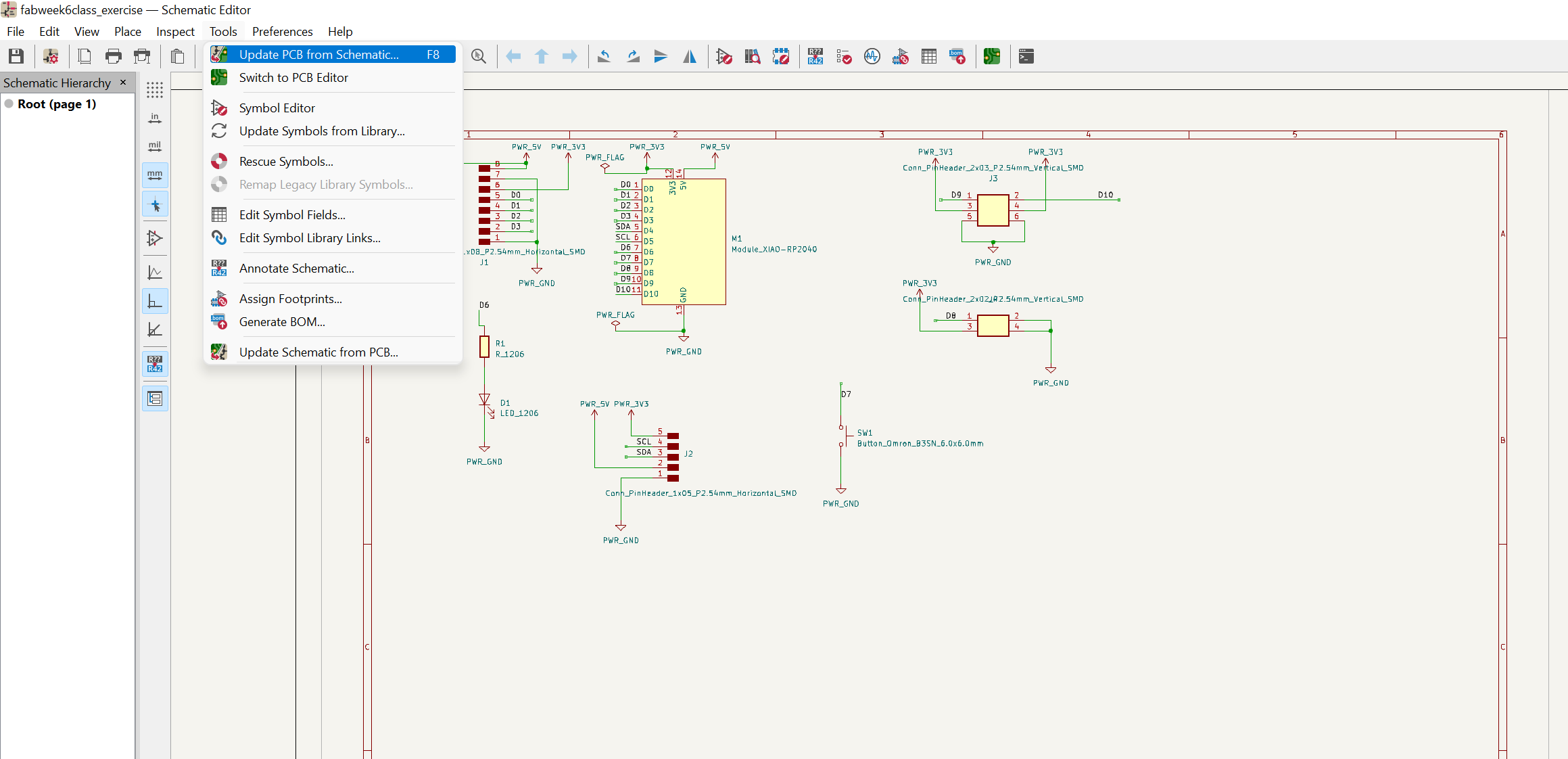
Then, “Update PCB from Schematics” option was chosen from “Tool” menu. Initially, there were some errors because there were a few unassigned labels hanging in the schamtics area.
Updating PCB from Schematics opened the kicad_pcb file, and then we had to move components in order and draw connections using routes. Initially, my routing resulted in the scenario where all pins which should get 3V power could not be connected to the 3V pin on the MCU. So, I needed to try different connection routes. I sought the assitance of our lab instructor Antti Mäntyniemi with this issue.
Specific routing wire width was suggested to be 0.400 mm during the local session. But I missed to use this width and ended up drwaing routes with default wire width.
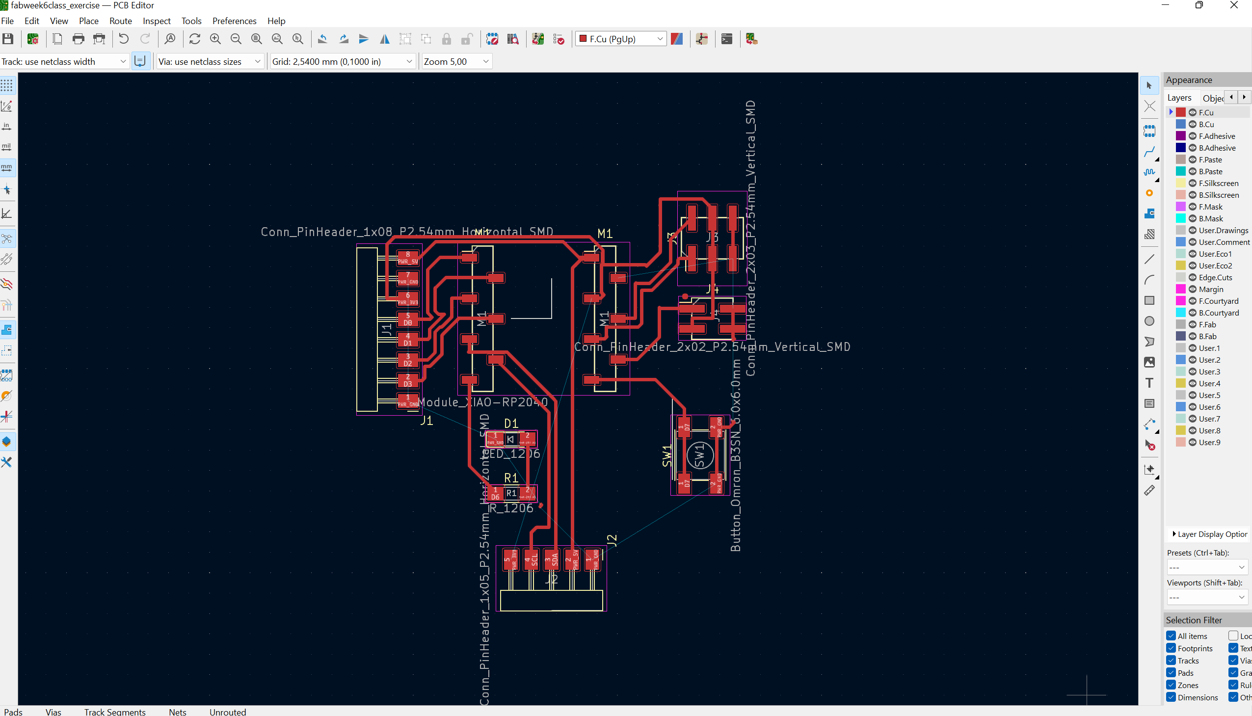
I moved the components in a better order, drew edges to the board, and routed the connections between the components. GROUND connections were connected at this stage since they were to connected after filling the zone.
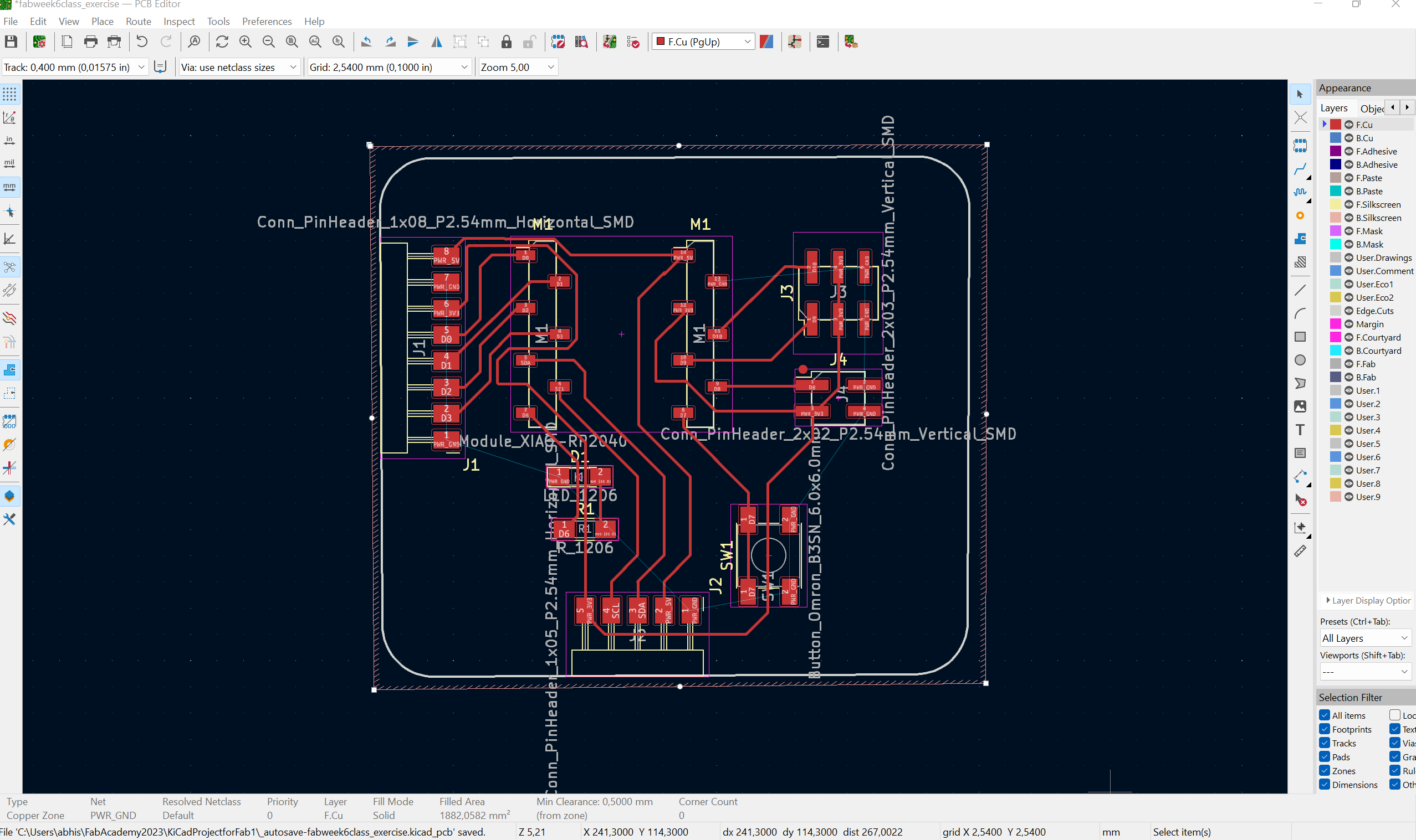
“Add a filled zone” from the right hand menu was selected and clicked inside of the board region. To add GROUND connections to the board, “F.Cu” from left was selected and PWR_GND from the list. It added copper (now in red color) to the board (in Fig 11), which was not there before (Fig 10). All red zone (copper filled) serves as medium for GROUND connection.
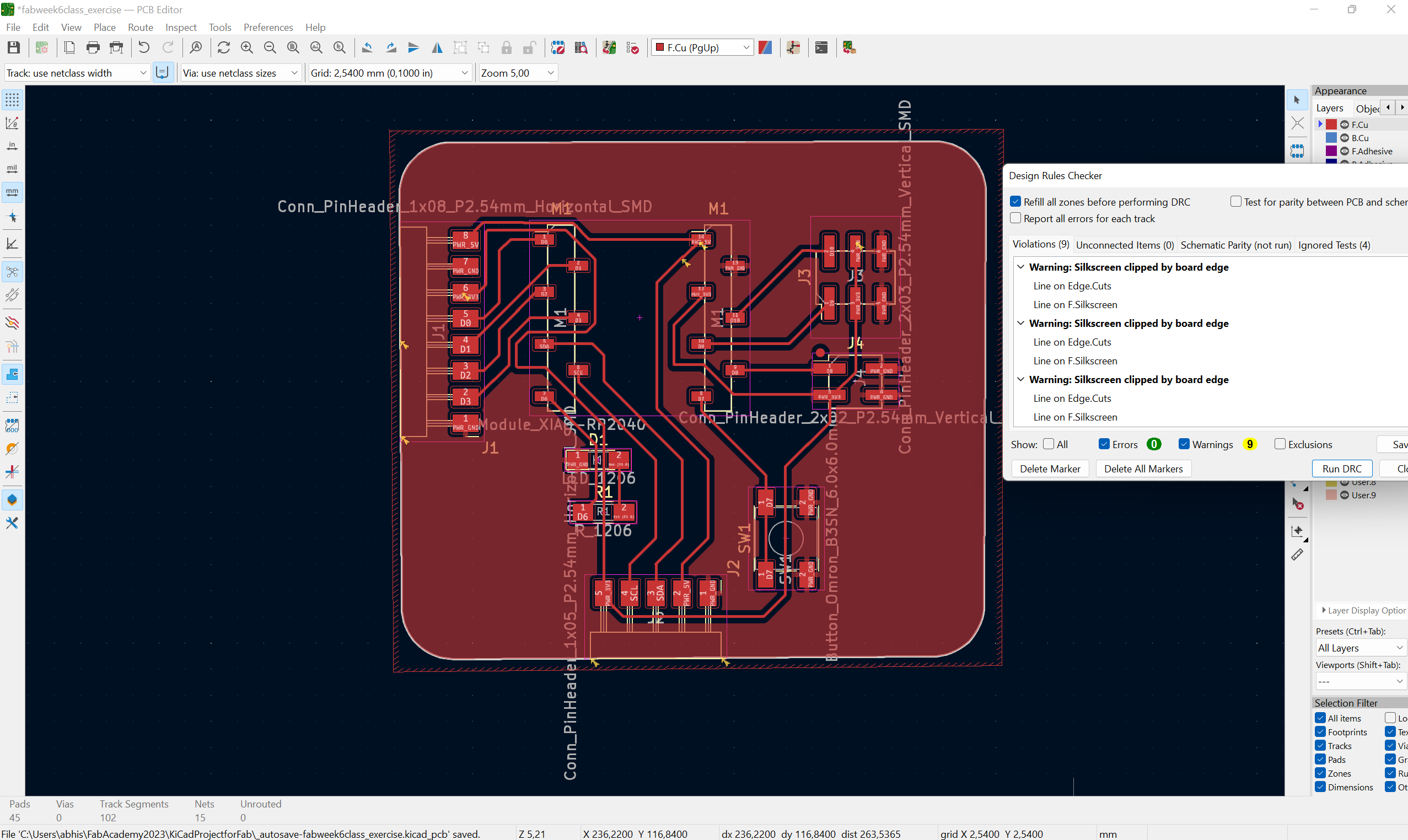
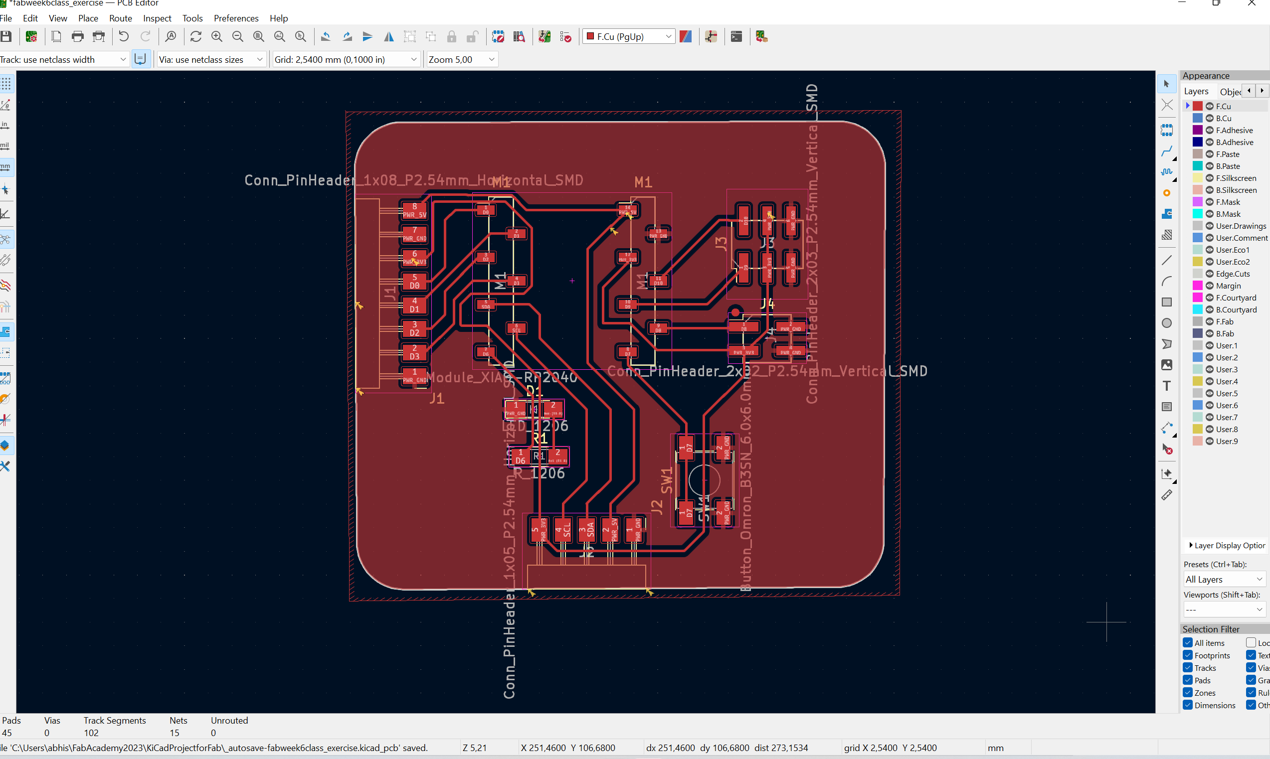
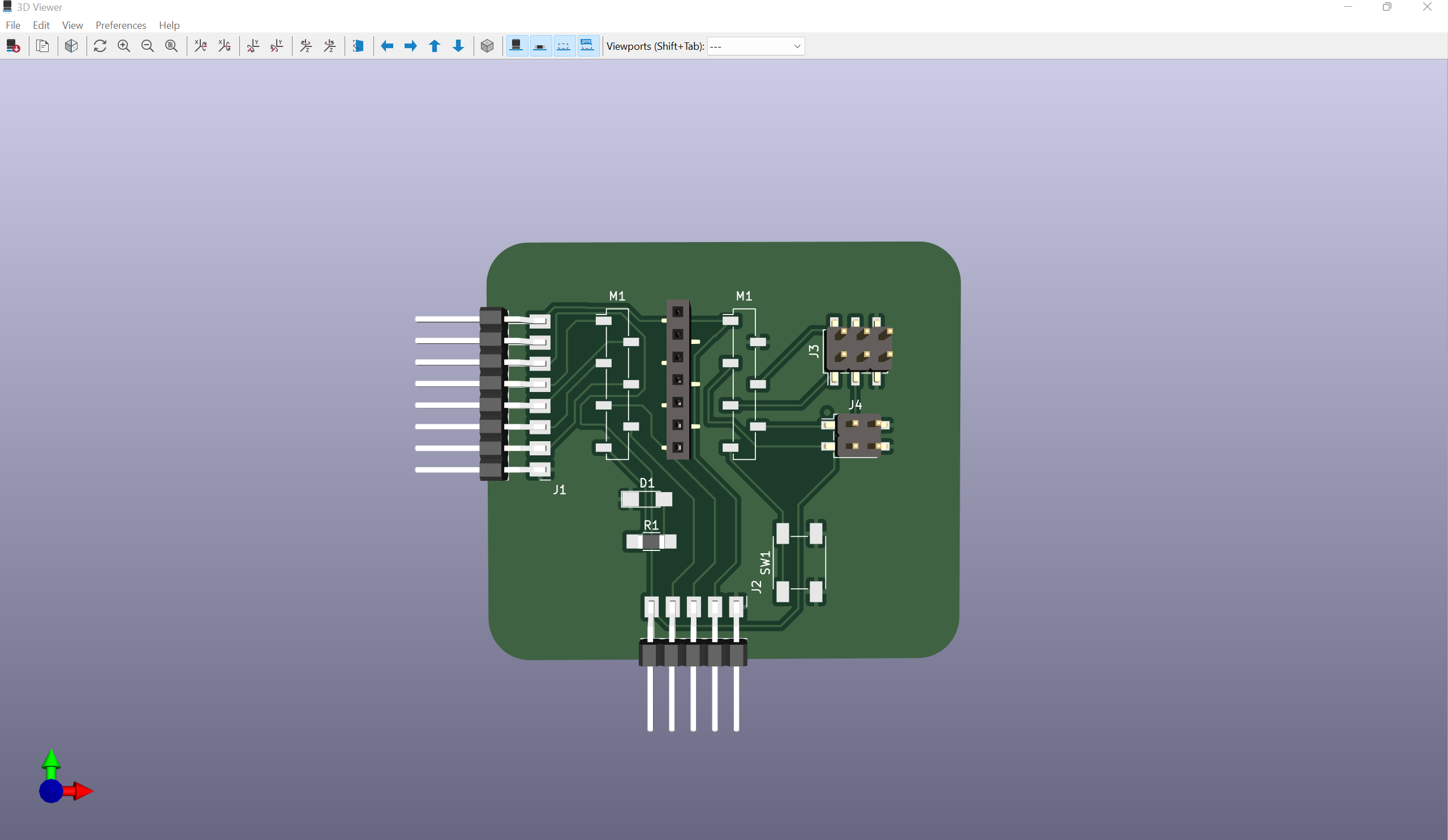
Figure 13 shows 3D View of the PCB. It can be selected via: View-> 3D Viewer in KiCad PCB layout window.
KiCad files can be found from here.