Electronics Design
KiCad
Fab components library
After installing KiCad, I also installed the library of components that should be available at fablabs. It's a great work done by Krisjanis Rijnieks. The library and the detailed instructions on how to install it, are available here

Schematics
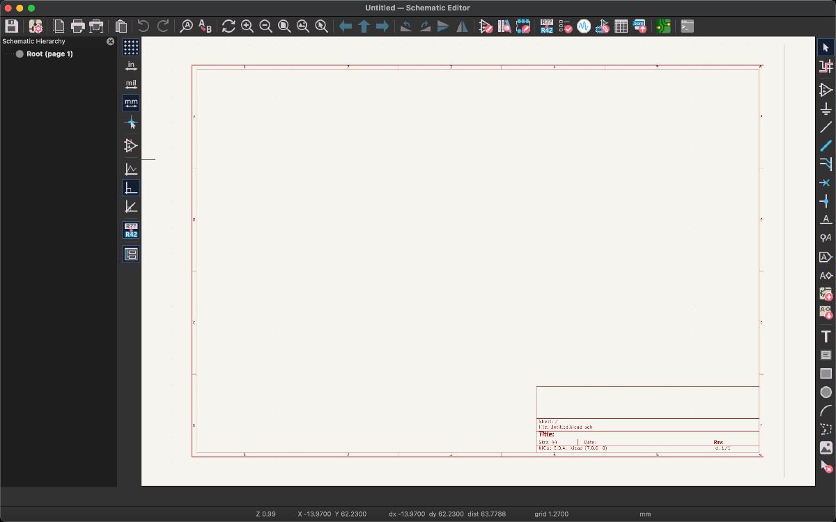
- This is what the software interafce looks like when starting a new project
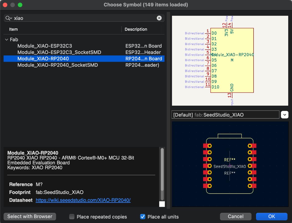
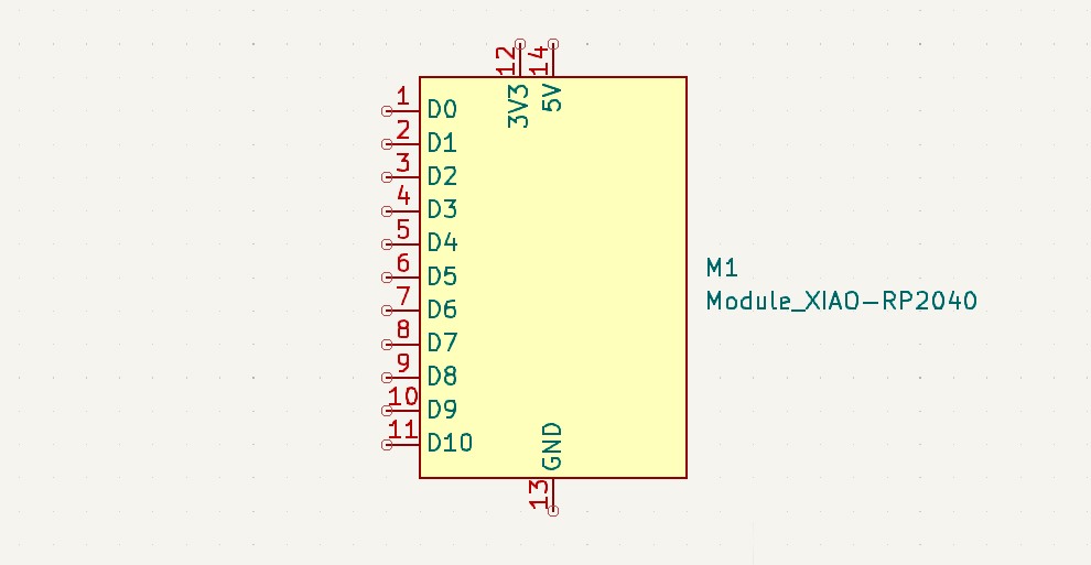
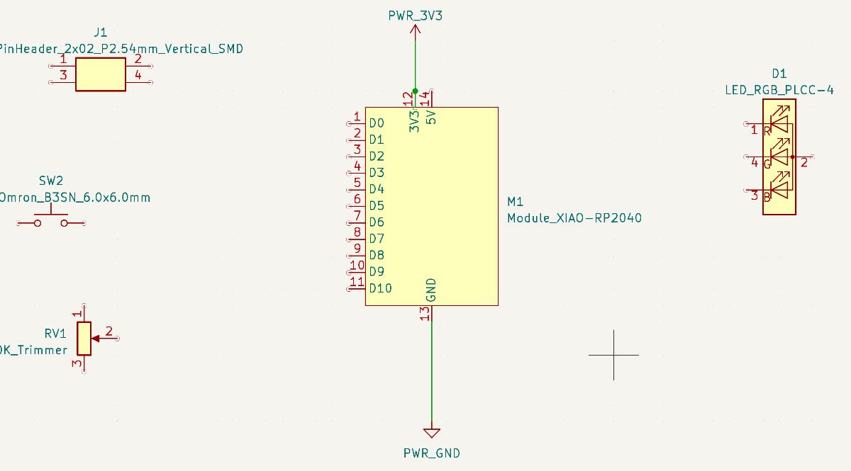
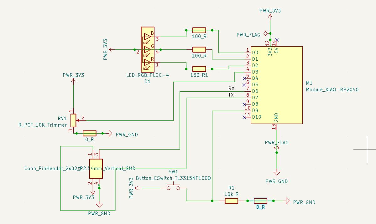
- The next step was to add all the necessary components. I did it with the Add a symbol (A) option that opened a new window.
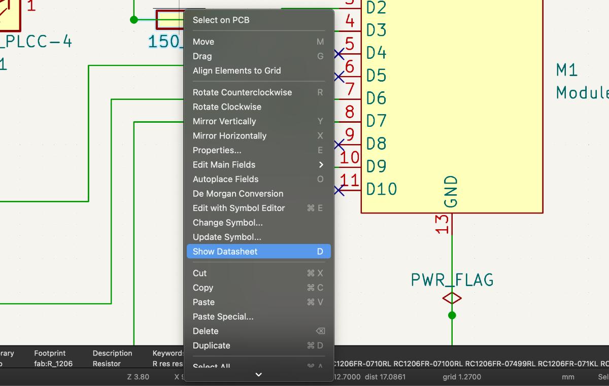
- The most important parameters of all the components may be found via the Show Datasheet (D) option accessible through the add symbol window an then by right clicking an already added component
- It is also possible to Edit Value (V) of the particular components
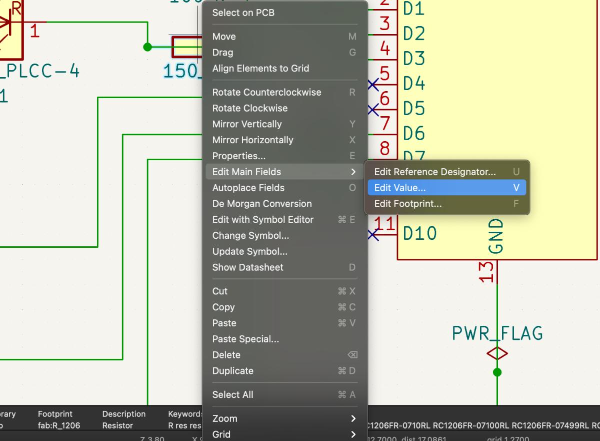
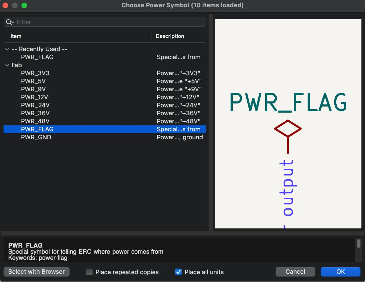
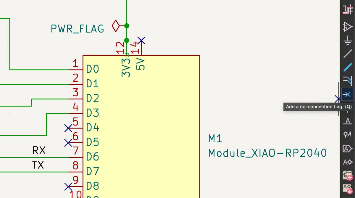
- The next step was to add a Power Symbol (P) that defined the power source and main ground for the whole circuit. It should be the special PWR_FLAG
- Then it was necessary to add the connection between specific components. It was done with the add Wire (W) option. It was not neccessary to connect all the components to the main Powr and Ground pins - I did it using the flags instead to make the schematic easier to read
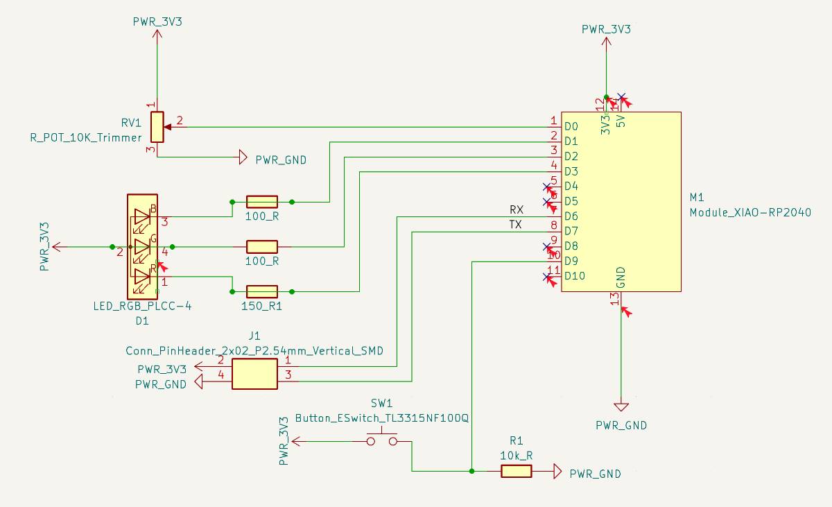
- There were some pins left without any wire. It was necessary to define them as unconnected with the No-Connection Flag (Q)
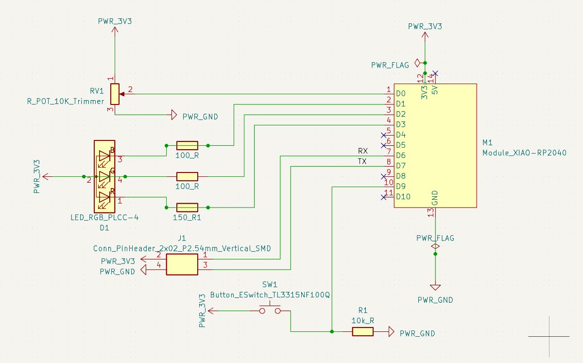
- This is what my schematic looked like after the steps above
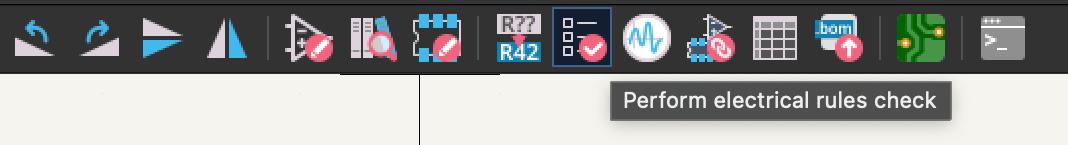
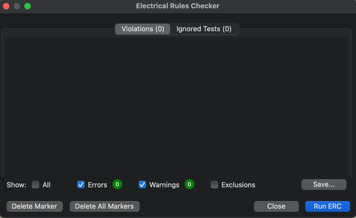
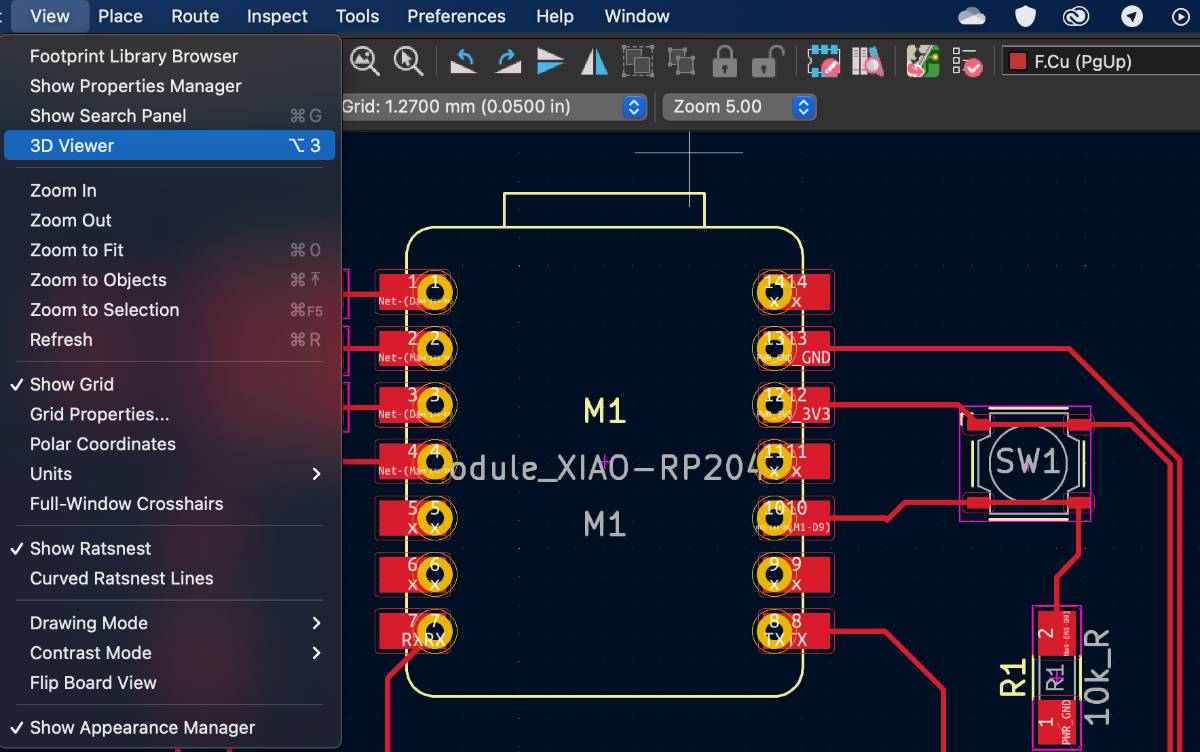
- I also performed the Electrical Rules Check on my board to ckech for any possible problems
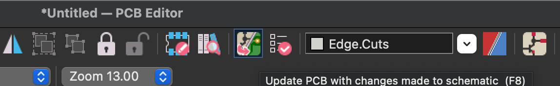
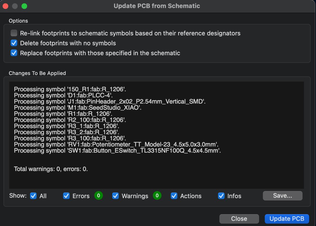
- First, I needed to transfer the components defined in the schematics to the board designer window. I used the Update PCB from Schematic (F8) option
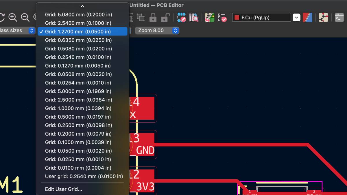
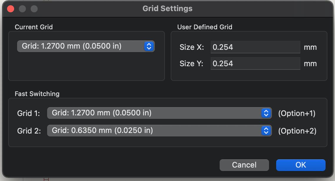
- Then I defined the Grid , that I wanted to use for my board. It is crucial to select fitting grid spacing for one's purpose
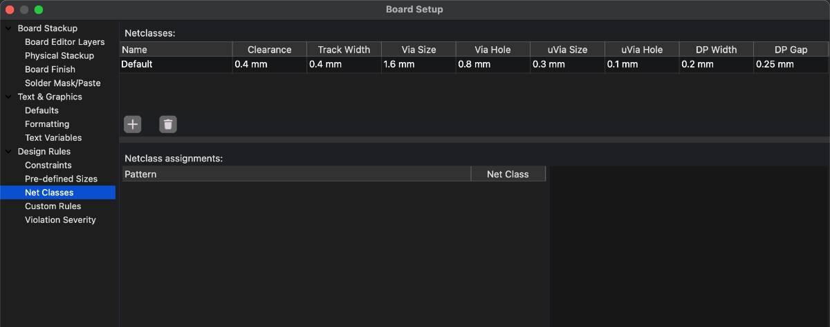
- I made changes to the default Board Setup options as listed above. It is another crucial step to perform in order to be able to fabricate the board later on. The parameters depend on the fabrication method.
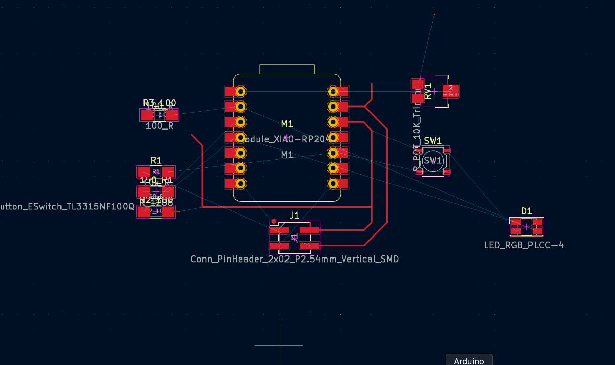
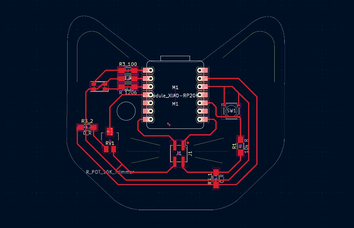
- I placed the components in the board viewer with no parcticular design in mind. It was the first time I wass doing this, so it was random. KiCad showed me where the connections should go with the thin blue lines

- I started adding Route Tracks (X) to connect the components
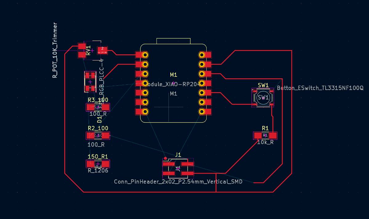
- And I got stuck. This particular board integrates a Seeed Xiao board that has a USB-C connector. I acknowledged that this connector should be placed by the edge of the board, so no routes could go there and it created a significant constraint in the circuit design. At some point I got so entangled in the route maze, that I could no longer proceed connecting the pins. I managed to get the signal and power connection to all the components, but could not connect the ground pins
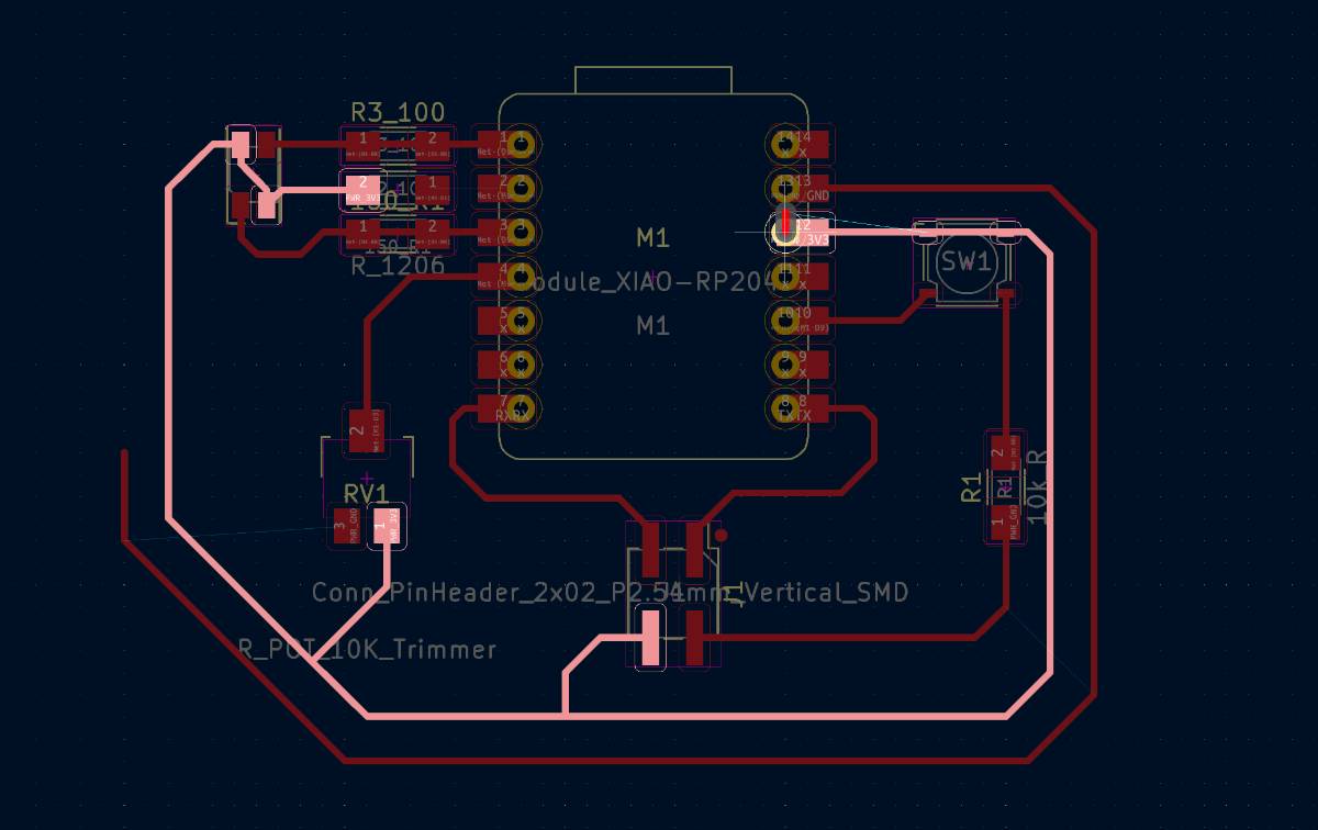
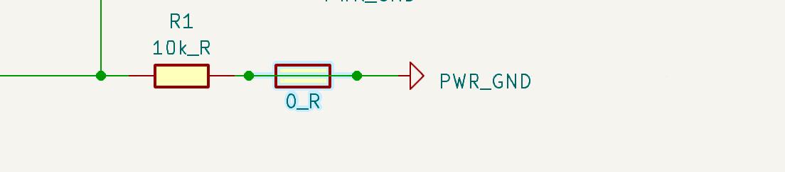
- Adviced by Kris, I added two Resistors with value 0 , serving as bridges that go over other routes. Another solution would have been to make the ground connection on the other side of the board, but I decided to go with the one-sided board as my first one

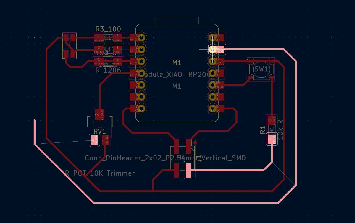
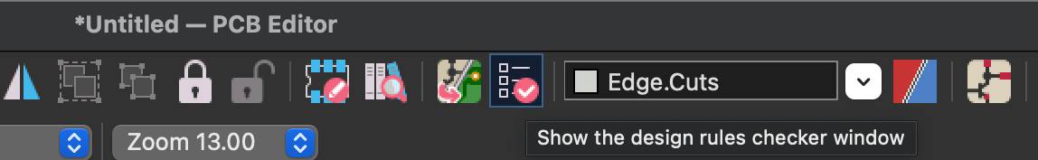
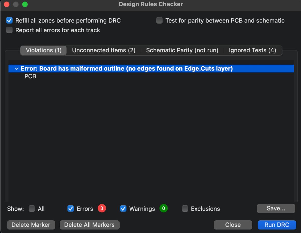
- The next step was to perform the Design Rules Check
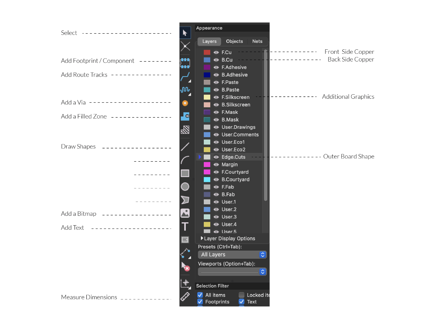
- In order to add the outer shape to cut the board in, I needed to switch to the Edge Cuts layer
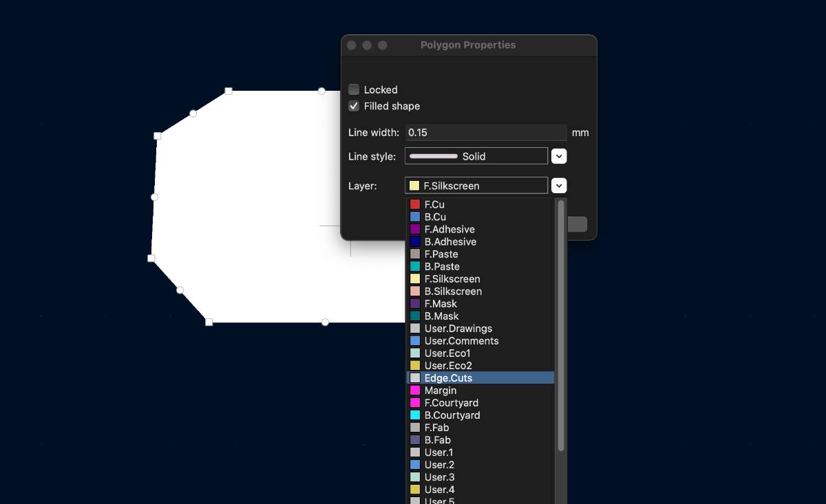
- I exported the route preview as an SVG file that I opened in Illustrator, where I drew the cat shape.
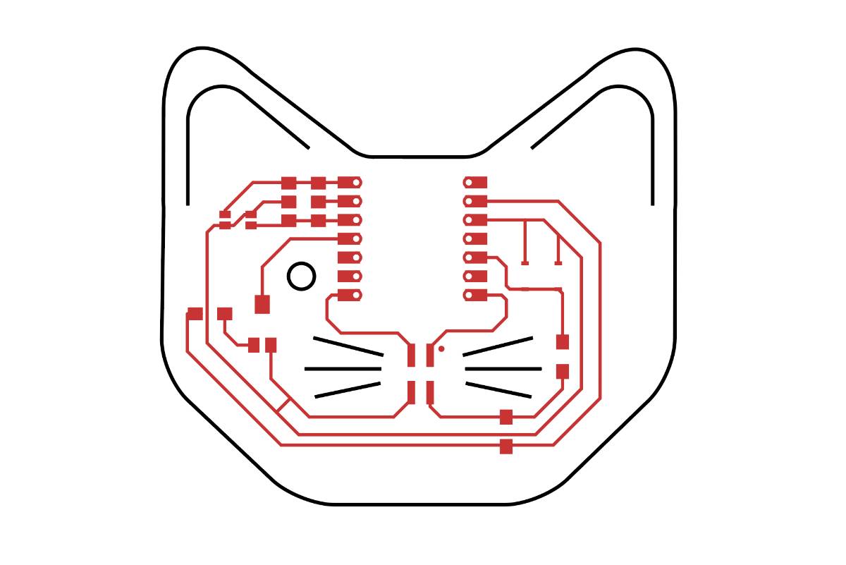
- I Imported the SVG Graphics cat shape to the Edge Cuts layer
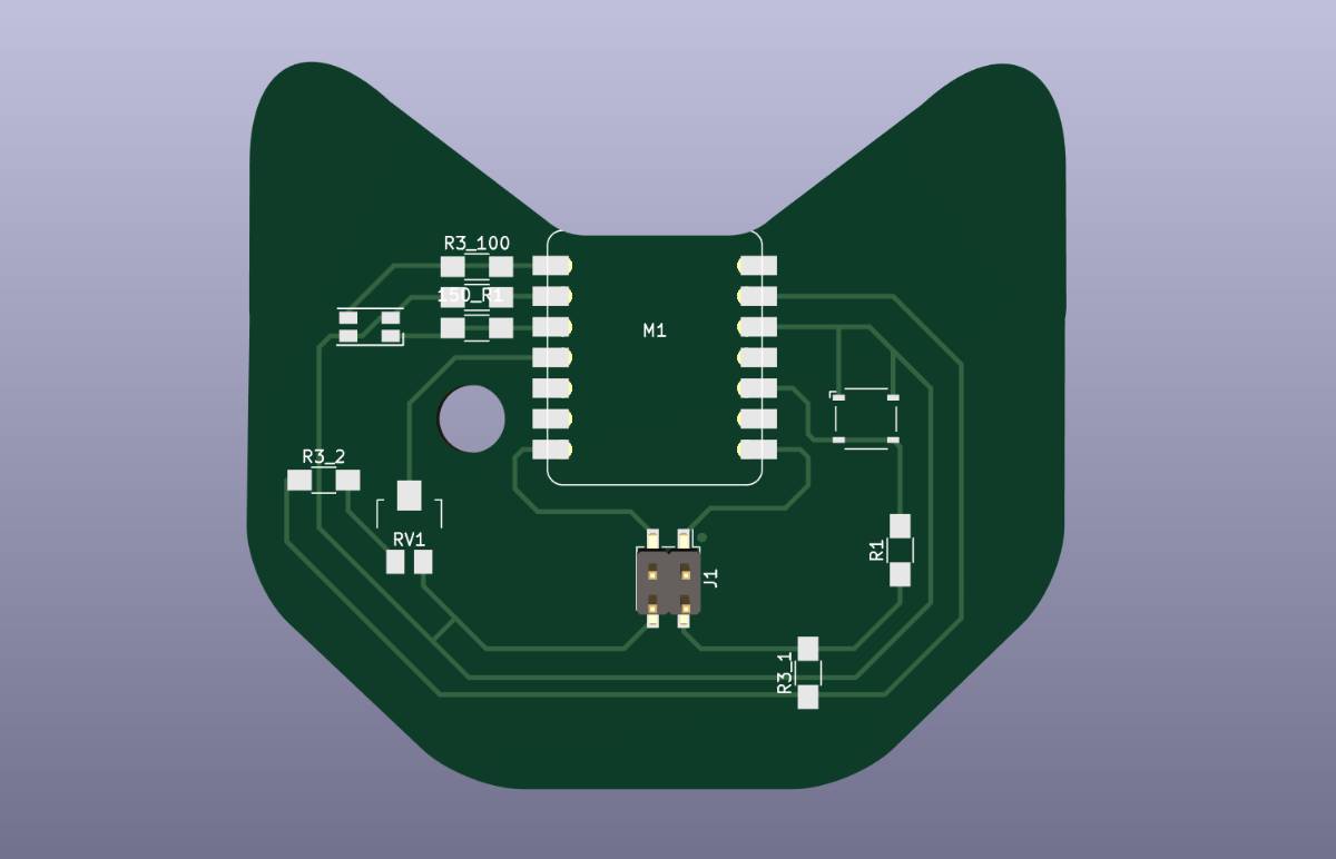
- I opened the 3D Viewer to see a rendered preview of what the board would lool like
Calculating the Resistor value needed for my RGB LED

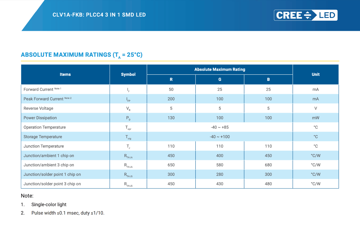
In order to calculate the resistance of a resistor needed, I opened the CLV1A-FKB: PLCC4 3 in 1 SMD LED datasheet to look up the following:
- Forward Voltage Drop (Vf) : the voltage drop across the LED when it is conducting current. Should be the typical or average value of Vf. ccording to the datasheet for the CLV1A-FKB, the typical forward voltage drop is 2.8V.
- Maximum Current (If) : maximum current that the LED can handle without being damaged. In the circuit it should be less than or equal to the maximum current specified on the datasheet. According to the datasheet, the maximum current for this LED is 20mA.
- Supply Voltage (Vs): voltage of the power supply. In my case is 3V3.
Then I used the Ohm's law (V = IR) to calculate the resistance needed for my circuit (where I is current, V is voltage, and R is the resistance). The voltage across the resistor should be the supply voltage minus the forward voltage drop of the LED (Vr = Vs - Vf). The current flowing through the resistor shuld be the desired current for the LED (If). So the formula for calculating the resistance needed shuld be
R = (Vs - Vf) / If
R = (3.3V - 2.8V) / 0.02A = 25ΩSo I would need a resistor with a value of 25Ω or the closest available value that is higher than 25Ω. This resistance calculation is based on the maximum current of the LED, and iit could be a lower current for a a dimmer light.
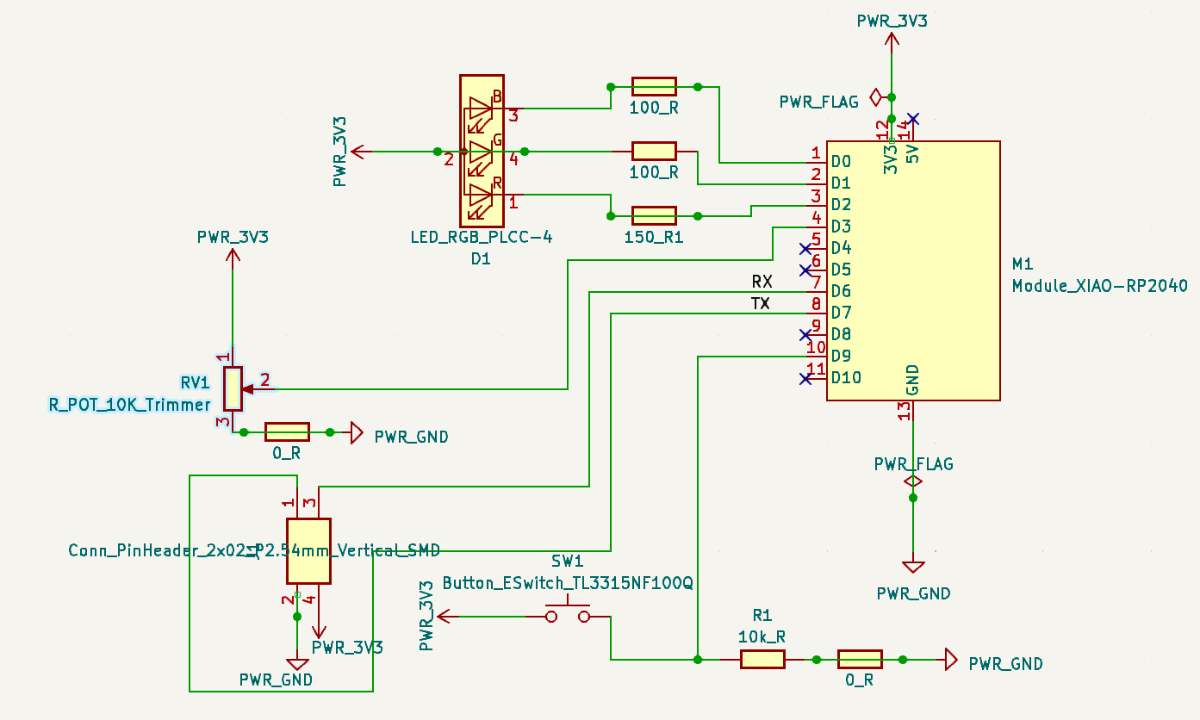
I will need to update the resistor values in my schematics for the 3V3 power supply instead of 5V
Group Assignment page
- I Imported the SVG Graphics cat shape to the Edge Cuts layer
Circuit design - board view
Then I could proceed with the next step - designing the board itself
The route labyrinth
Layers
Outer shape
Everything may be made into a cat,
if you try hard enough