14. Networking and communications
Hello! In this opportunity, we will learn about networks and communications.
A very important part is the communication between devices and/or projects, we must know the two communication methods, SPI and I2C.
Research
SPI (Serial Peripheral Interface)
The SPI Bus is a communications standard, used mainly for the transfer of information between integrated circuits in electronic equipment. The Serial Peripheral Interface Bus or SPI bus is a standard for controlling almost any digital electronic device that accepts a clocked serial bit stream (synchronous communication).
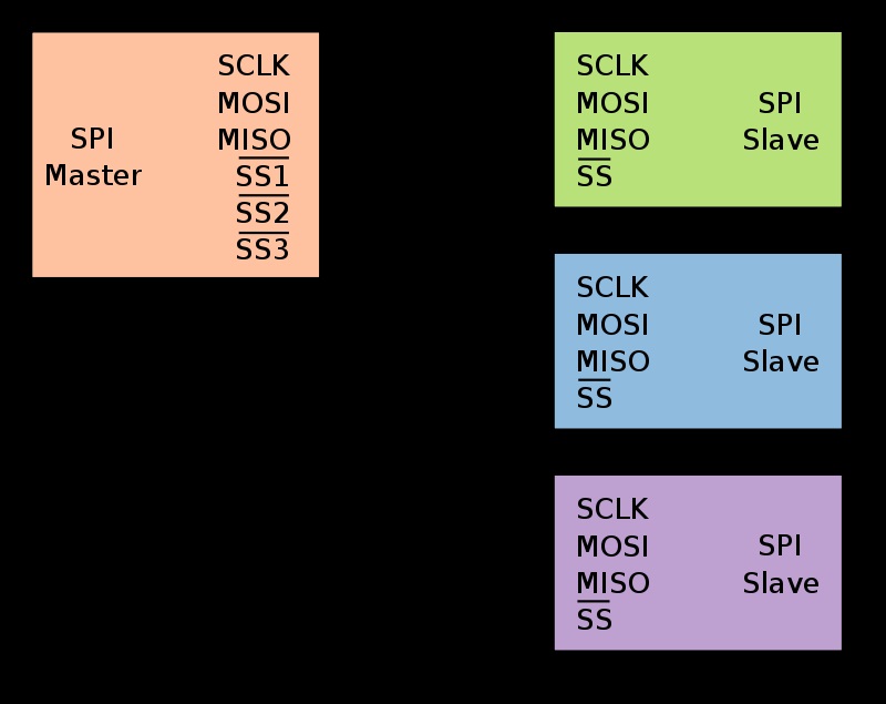
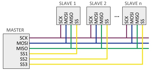
It includes a clock line, data in, data out, and a chip select pin, which turns on or off the operation of the device with which one wishes to communicate. In this way, this standard allows multiplexing the clock lines.
Many digital systems need a fast connection to their peripherals. The advantages of a serial bus is that it minimizes the number of conductors, pins, and the size of the integrated circuit. This reduces the cost of manufacturing, assembling and testing the electronics. A serial peripheral bus is the most flexible option when you have different types of serial peripherals. The hardware consists of clock signals, data in, data out and chip select for each integrated circuit that has to be controlled. Almost any digital device can be controlled with this combination of signals. Devices differ in a predictable number of ways. Some read the data when the clock goes up, others when the clock goes down. Some read it on the rising edge of the clock and others on the falling edge. Typing is almost always in the opposite direction of the direction of movement of the clock. Some devices have two clocks. One to capture or display the data and the other to the internal device.
OPERATION:
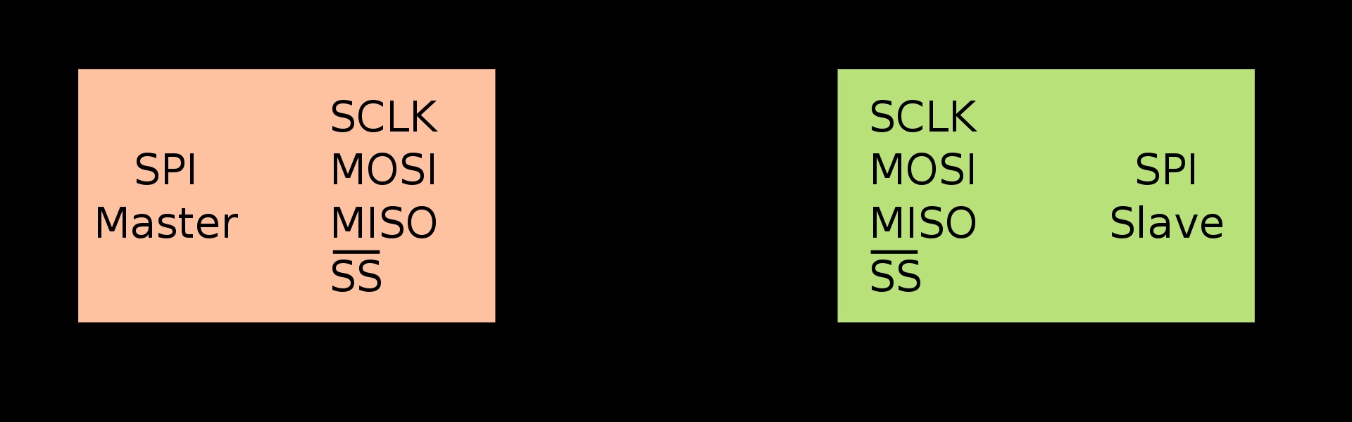
SPI is a synchronous protocol. Synchronization and data transmission is carried out by means of 4 signals:
- SCLK (Clock): It is the pulse that marks the synchronization. With each pulse of this clock, one bit is read or sent. Also called TAKT (in German).
- MOSI (Master Output Slave Input): Data output from the Master and data input to the Slave. Also called SIMO.
- MISO (Master Input Slave Output): Data output from the Slave and input to the Master. Also known by SOMI.
- SS/Select: To select a Slave, or for the Master to tell the Slave to activate. Also called SSTE.
The String of bits is sent synchronously with the clock pulses, that is, with each pulse, the Master sends one bit. To start the transmission, the Master lowers the SSTE or SS/Select signal to zero, with this the Slave is activated and the transmission begins, with a clock pulse at the same time that the first bit is read. Note that the clock pulses can be programmed in such a way that the transmission of the bit is carried out in 4 different modes, this is called polarity and phase of the transmission:
- With the rising edge without delay.
- With a delayed rising edge.
- With the falling edge without delay.
- With a delayed falling edge.
I²C DEVICE
The original system was developed by Philips in the early 1980s in order to easily control various chips in televisions. Since the mid 1990s I²C is also used by some competitors to designate Philips I²C compatible systems, including Siemens AG (later Infineon Technologies AG), NEC, STMicroelectronics, Motorola (later Freescale), Intersil, etc. There are a total of one thousand different ICs from more than 50 manufacturers (according to 2014 data).
ELECTRICAL DEFINITION:
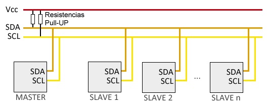
Three devices are represented in the diagram. The I²C requires two signal lines: clock (SCL, Serial Clock) and the data line (SDA, Serial Data). Both lines require pull-up resistors towards VDD. Any device connected to these lines is drain or open collector (Open Collector), which in combination with the pull-up resistors, creates a Wired-AND circuit. The high level must be at least 0.7 x VDD and the low level must not be more than 0.3 x VDD. The series resistors Rs (not represented in the diagram), at the input of the devices, are optional and are used as protection resistors. The I²C Bus works with positive logic, this means that a high level on the data line corresponds to a logical 1, and a low level to a 0.
BUS STATUS PULSE:
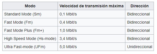
The clock signal is always generated by the master. For each specified mode, a maximum allowable clock pulse is respectively predetermined. In general, slower clock signals can also be used, as long as they are compatible with the master interface. However, some integrated circuits (for example, an analog-to-digital signal converter or converter) require a minimum frequency in order to function properly. The following table shows the maximum allowable clock percentages.