Electronics design
This week there are two types of assignments, one group and one individual. In my case I’m alone in ESNE’s Fab Lab so I am doing both.
Assignments
Group assignment:
- Use the test equipment in your lab to observe the operation of a microcontroller circuit board.
Individual assignment:
- Redraw an echo hello-world board, add a button and LED check the design rules, make it, and test that it can communicate.
Group assignment
Group assignment page
In the following link you can access the Leon Fab Lab page that contains all the group assignments: Fab Lab Leon group assignment page
Measurement tools
When working with electronic products, certain tools allow us to understand what is happening in our circuits, if there is voltage or not, what resistors we have, or capacitors… or if there is continuity in our tracks.
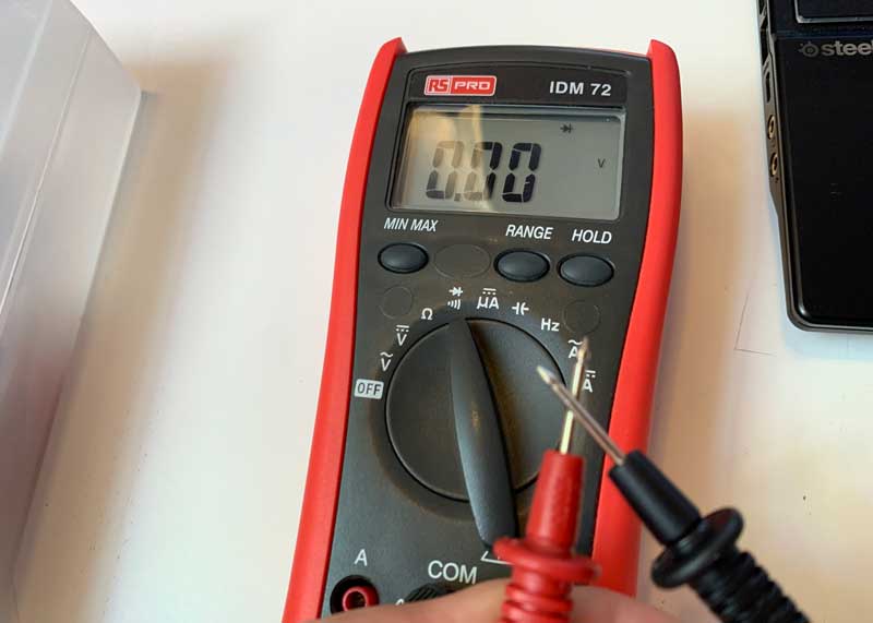
Multimeter
I use a multimeter of the brand RS Components. It is not the cheapest multimeter in the market but it works well. The multimeter seems to me the most useful tool in the field of electronics because I normally use it for various things.
Continuity
The first use that I give it is in the way in which the multimeter emits sound when there is continuity between the two poles, it is very useful to know if there is a damaged cable or if the tracks of a pcb are connected or not
Resistances
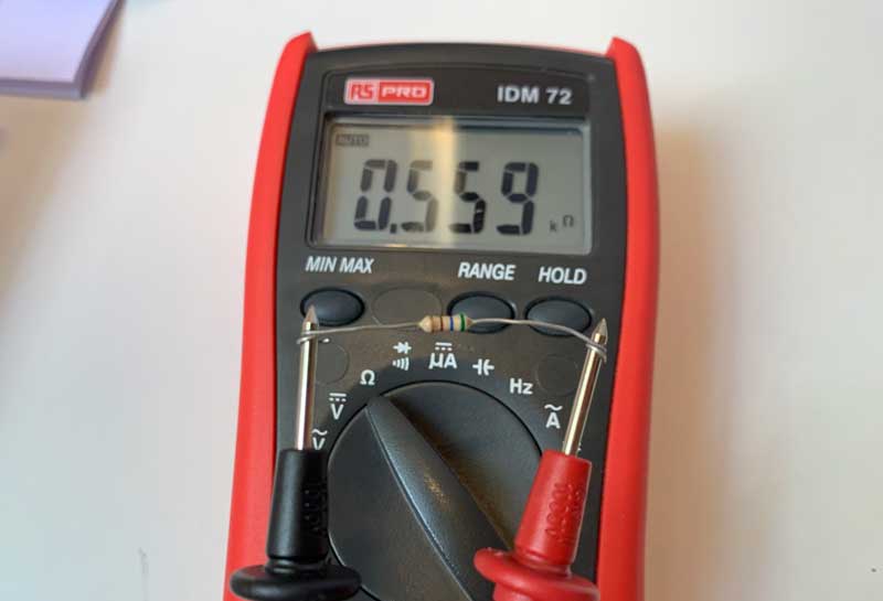
The second mode that I use the most is the measurement of resistances, whether they are SMD or Through Hole.
Polarity
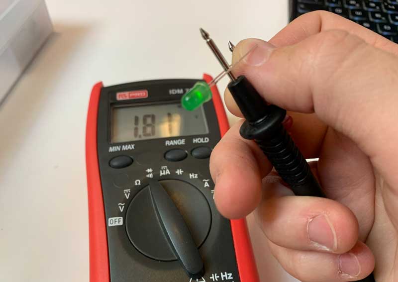
The third mode that I use the most is to know the polarity of certain components such as LEDs, in my multimeter it is in the same tab as continuity but you have to change the mode
Individual assignment
Install Kicad and libraries
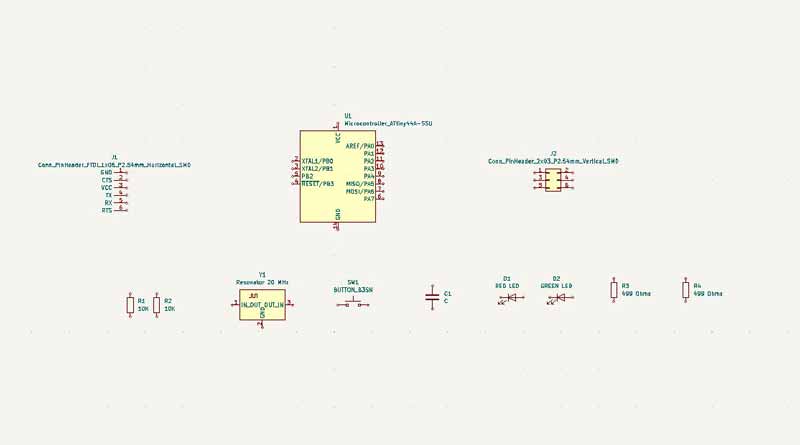
For individual assignement I started by downloading Kicad to do the PCB design. After that I downloaded the Fab electronics component library for KiCad.
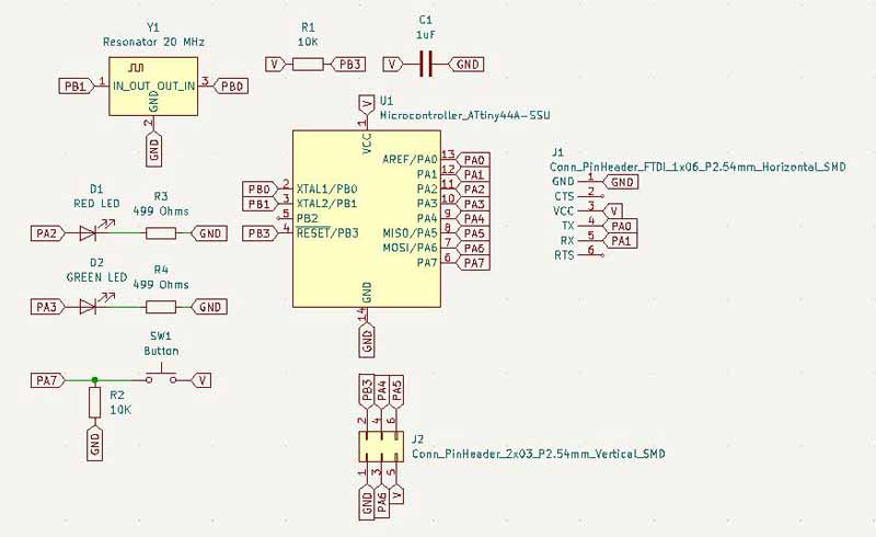
After a couple of failed attempts I managed to successfully install all the libraries. Then I put all the components I had to make my board into Kicad’s schematic editor.
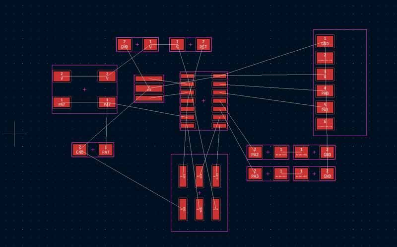
First steps in Kicad
Then I went to the board editor to see where I could pass the paths of each of the components, after trying 50 times and not succeeding, I copied the paths from this link.
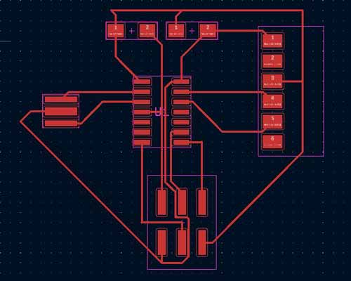
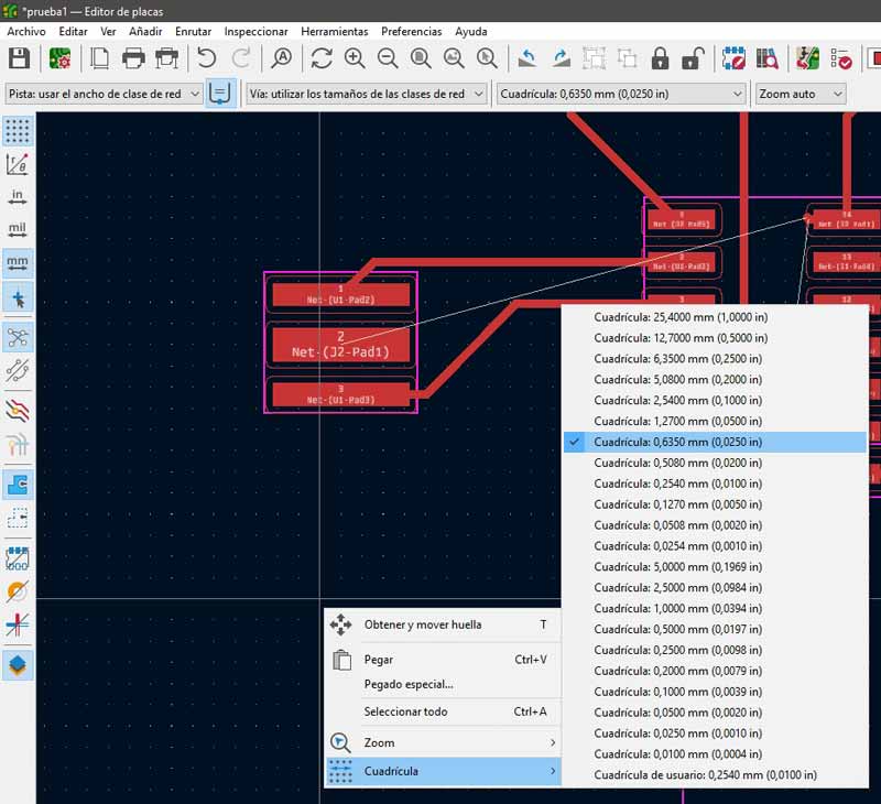
At the beginning I had many problems with the distance between different paths, I was able to solve it by reducing the size of the reference mesh that Kicad has by default, when I reduced the size of the mesh I was able to pass the paths where I needed without problems.
Try to design the paths leaving the maximum possible distance between them to avoid problems when milling the plate.
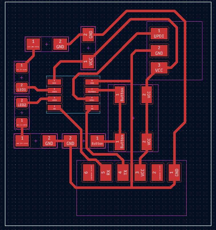
Now that I had connected everything and tested the two ways Kicad works, I went back to the schematic editor to connect the button, the leds and the resistors.
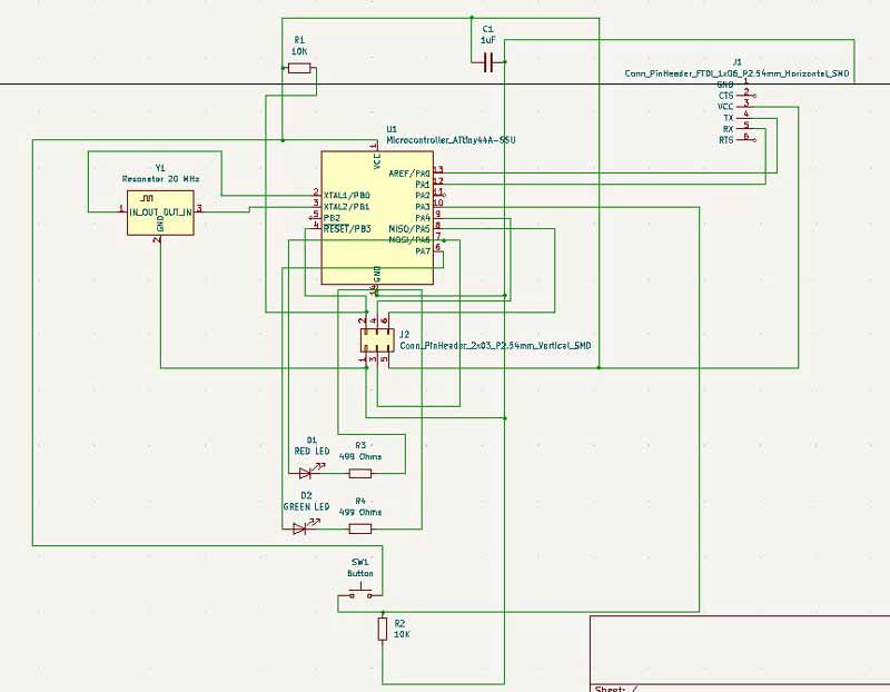
With all the cables the schematic editor was very confusing. I changed everything to labels, it was a good decision, the schematic is much cleaner and easier to understand.
Then I went on to connect the components but I had problems connecting all the pads, I couldn’t find a way to connect them all.
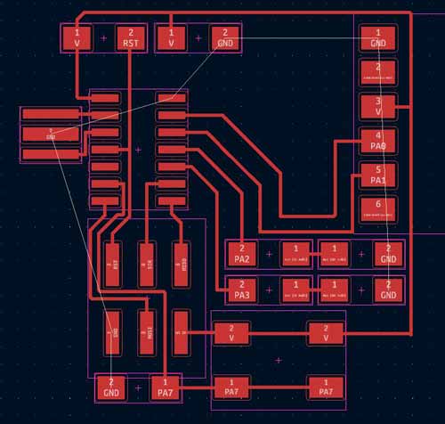
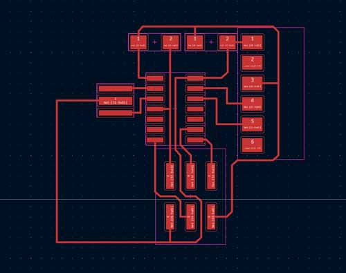
On Sunday morning I spoke with my colleague Luis Diaz, Luis taught me how to make a square on my board to connect all the GND, he also told me to avoid making 90º angles in the paths and to change the thickness of the paths to 0.4 and 0.8. After making all these changes my board was ready to export.
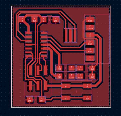
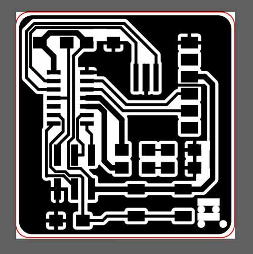
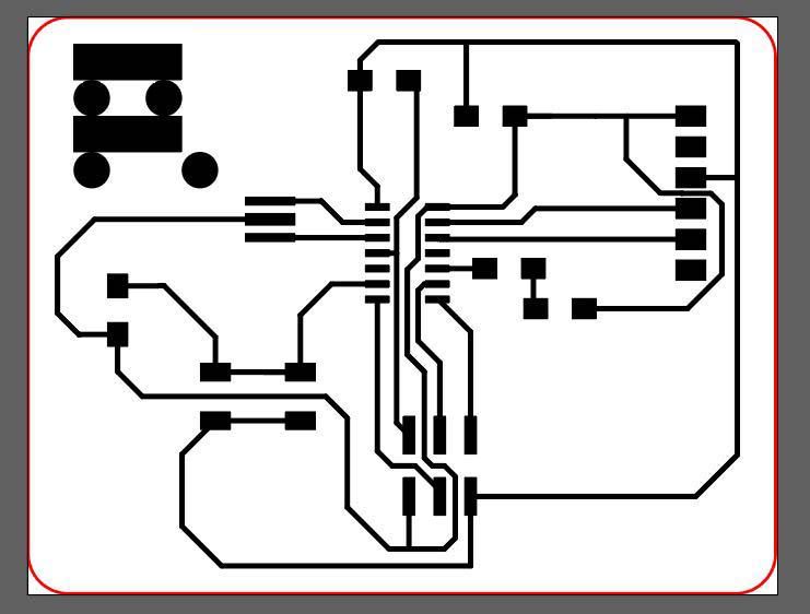
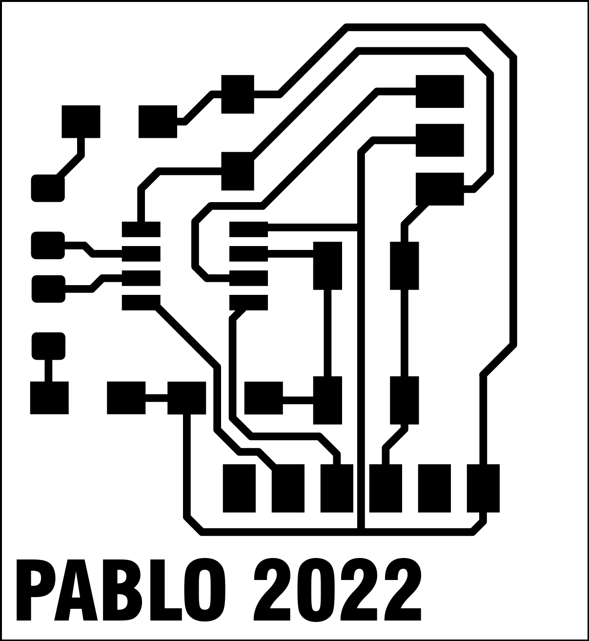
After exporting it in .svg I opened it with Illustrator to modify the paths a bit and customize my plate, I wanted to remove parts of the plate that I did not like, round the corners of the plate and add a drawing somewhere.
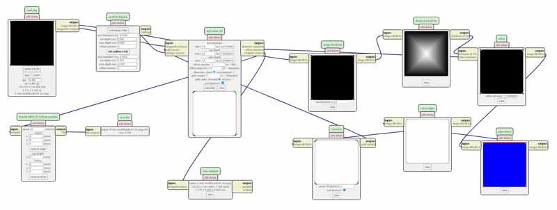
Gcode in mods
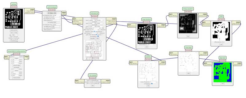
Then I passed the svg to mods to create the gcode for the Roland, I was able to make the gcode for the milling of the paths without problems.
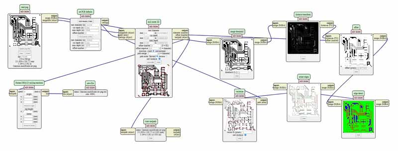
But to mill the outline of the plate, mods made the file disappear and I couldn’t get it to calculate the gcode. I tried to do it with the svg as with the png but I didn’t get anything.
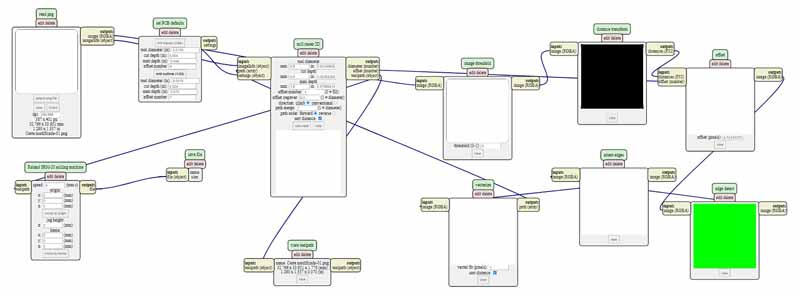
Then I realized that the previous file was wrong and I wanted to mill the opposite, the same thing happened with the contour. I modified the .png’s in Photoshop and redid the gcode with mods. I hope this time it works on the milling machine.

Problems with mods
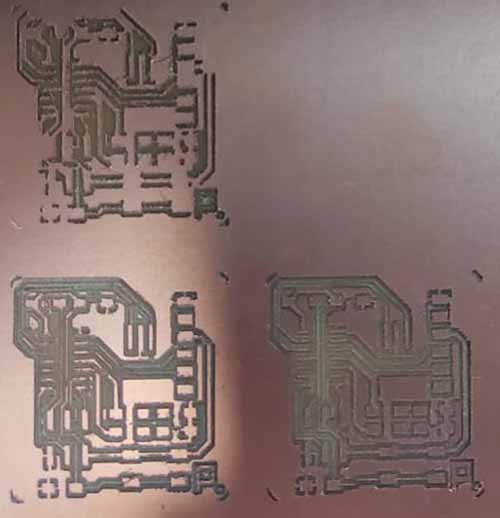
But with the gcode I made in mods, the milling machine eliminated one of the paths that passed under the microcontroller, I tried several times with different milling cutters but I couldn’t mill any plate that worked
I decided to change the design of the plate to see if with another design I could mill a plate that would work, I erased all the paths I had made in Kicad and started over again
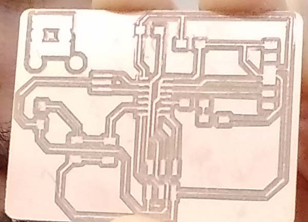
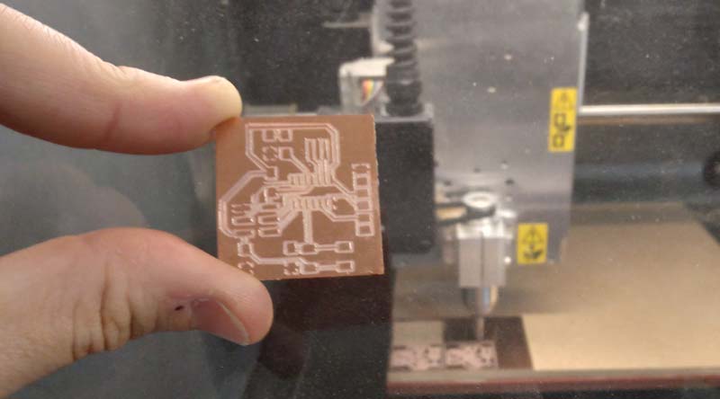
I added a logo to this last design and milled it on the milling machine
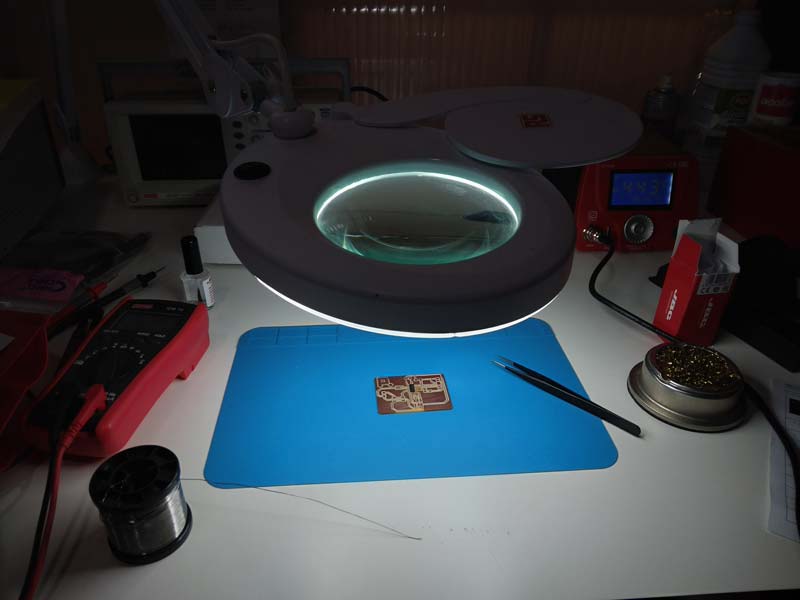
Then solder the components to the board starting with the microcontroller

Problems soldering the plate
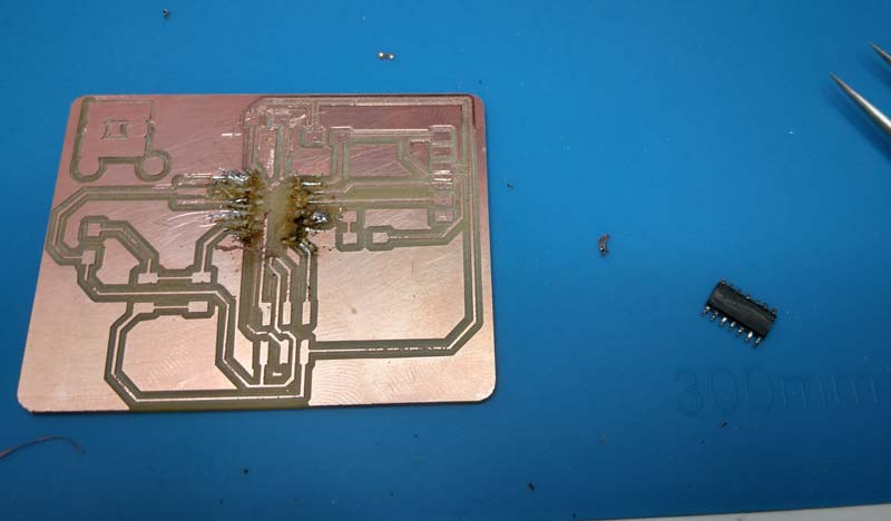
When soldering the microcontroller I had continuity problems because there was tin under the microcontroller joining two paths, so I had to desolder the microcontroller and mill another board again :(
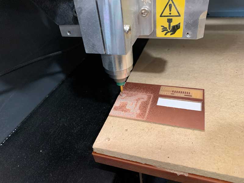
Problems milling the plate
I tried milling a board design that my colleague Luis Diaz gave me to see if it worked better for me when I soldered the components on the board
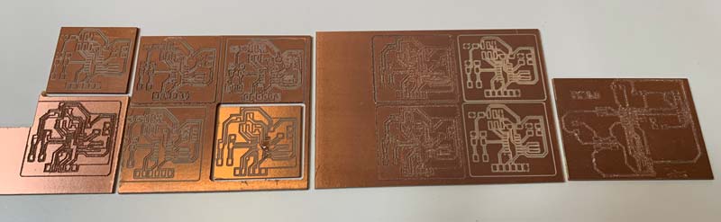
In the process of milling the plate, in addition to the previous problems, I had many other problems with my milling machine. In the following photo you can see the number of poorly made plates that I manufactured. Finally, all these problems were solved when the piece arrived with the 3mm head to use the 0.4 and 0.8mm diameter milling cutters.
No more problems, Hello ATtiny412
After receiving in the fablab the part for my milling machine with which I could put the 0.4mm and 0.8mm milling cutters, all my problems disappeared.
This time I designed a board for the ATtiny412 with two leds and a button, I started with the design in Kicad
Then pass the design through photoshop to transform it into png and add my name to the plaque
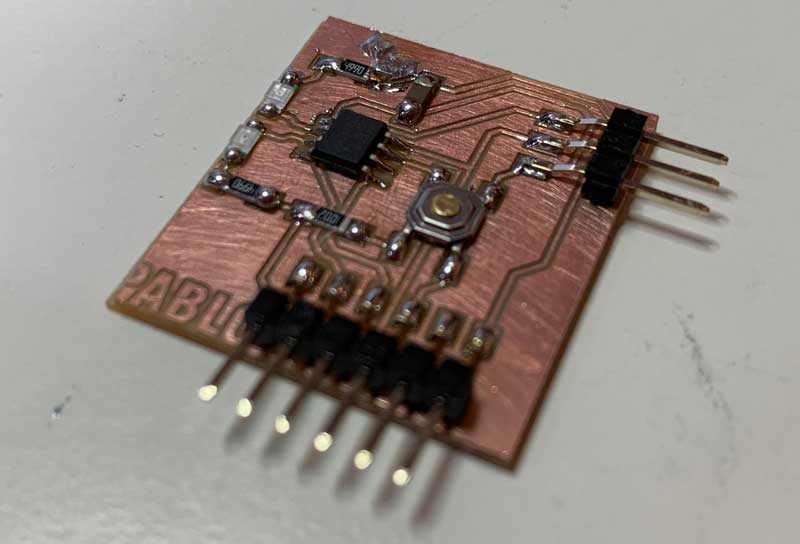
Then drill the paths with the 0.4mm drill and then the contour with the 0.8mm drill. The plate was perfect at first.
Finally I soldered all the components to the board, when I finished I had continuity problems between VCC and GND, checking the solder with the multimeter I discovered a ball of tin that was connecting two paths, luckily I was able to remove the excess tin and correct the problem of continuity
With all the components soldered I made a simple program for the board in which when pressing the button the green light would change to red and then back to green. This is the program I used on arduino
// Code for Hello ATtiny 4412 with 2 leds and 1 button
//By Pablo Pastor Fabacademy 2022

int ledR = 0; // LED RED
int ledG = 1; // LED GREEN
int boton = 4; // Button

int presionado = HIGH;

void setup() {

  pinMode(ledR, OUTPUT);  // initialize digital pin Led Red
  pinMode(ledG, OUTPUT); // initialize digital pin Led Green

  pinMode(boton, INPUT); // initialize digital pin Button
}

void loop() {

  digitalWrite(ledR, HIGH);   // turn the LED Red on
  digitalWrite(ledG, LOW); // turn the LED Green off

  presionado = digitalRead(boton);

  if (presionado == HIGH) {

    digitalWrite(ledR, LOW);   // turn the LED Red off
    digitalWrite(ledG, HIGH);  // turn the LED Green on
    delay(1000);

  }

}
I was able to upload my code without problems and check that my board was working correctly
Download archives
Kicad + PNG + Mods in the ATtiny412
See you next week!