6. ELECTRONIC DESIGN
This week we’re learning electronic components, the basics of an electronic circuit, and how to design and connecting them using copper or wire as a closed loop (such as resistors, capacitors, microcontrollers in through electrical current flow).
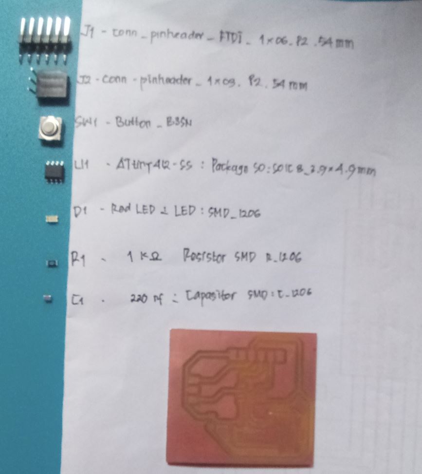
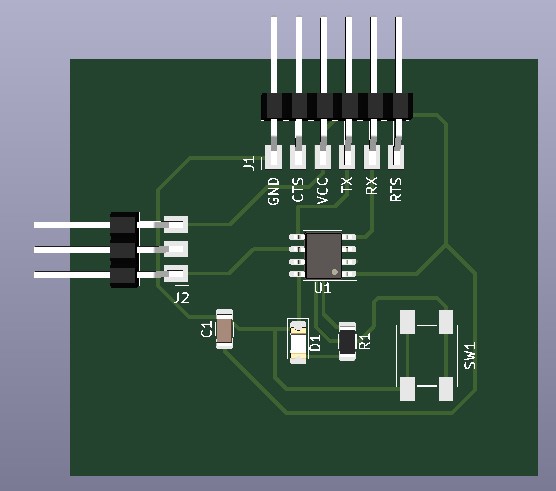
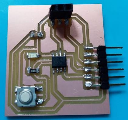
We’re working with SMD (surface mount device), components 1206 standard, and small components which has a high level of difficulty for me in placing it on the PCB and soldering them for ATtiny 412” hello-world board with a button.
ASSIGNMENT FOR THIS WEEK
Group assignment:
-
We use the test equipment in our lab to observe the operation of a microcontroller circuit board (in minimum, check operating voltage on the board with multimeter or voltmeter and use oscilloscope to check noise of operating voltage and interpret a data signal).
-
Document our work to the group work page and reflect on our individual page what you learned.
For group assignment, you find them in HERE.
Individual Assignment
- Redraw one of the echo hello-world boards.
- Add a button and LED (with current-limiting resistor) or equivalent input and output.
- Check the design rules, make them, and test them (simulate their operation).
LEARNING PROCESS
SMD components (Surface Mount Devices) are the electronic function parts, which are soldered to the circuit board by surface mount technology. There are many types of SMD components, and each type is packaged in different forms, which results in the huge SMD components library.
According to the function of SMD components, they can be classified as follows, the letters in brackets represent their identification on the PCB.
- Resistor
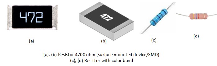
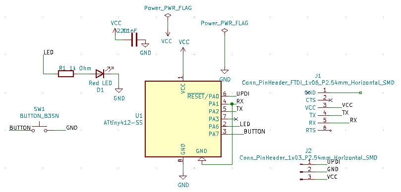
Chip Resistor (R), generally, the three digits on the body of a chip resistor indicate its resistance value. Its first and second digits are significant digits, and the third digit indicates the multiple of 10, such as “103’‘ indicates “10KΩ”, “472” is “4700Ω”. The letter “R” means “resistance”…I would describe a resistor as a component to reduce current.
- Capacitor
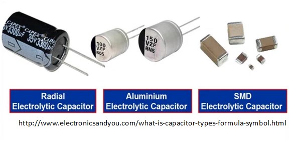
Capacitor (C), the most used are MLCC (Multi-layer Ceramic Capacitors), MLCC is divided into COG (NPO), X7R, Y5V according to the materials, of which COG (NPO) is the most stable. I would describe “capacitor”…as a device to temporarily store electrical charge.
- Diode / LED

LEDs are divided into ordinary LEDs and high-brightness LEDs, with colors of white, red, yellow, and blue, etc. The determination of LEDs’ polarity should be based on a specific product manufacturing guideline and it allows the current to only flow in one direction.
- Microcontroller

For this assignment, I used ATtiny412 for microcontroller. It is basically a small computer or integrated circuits, meaning that all the components are hidden inside. microcontroller requires protection against moisture are packed, together with absorbent and humidity sensor, in hermetically sealed Moisture Barrier Bags (MBB). It has no working memory so I can’t store anything on it, and there’s no operating system on it.
- Pin Headers
-
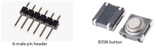
I used 6 pins header (male) able to connect electronic boards and other components to each other and 3 pin connector (female); because I ran out of stock pin header female as a connector.
- Button
I used a SWf B3SN button or a switch for a connection when we press to turn on the LED.
The picture of those components were listed in this picture below.
Making a Hello World Board
For our individual assignment this week we need to (re)create a “Hello World” board, based on the ATtiny412 blink board, but also add a button, and LED to it.
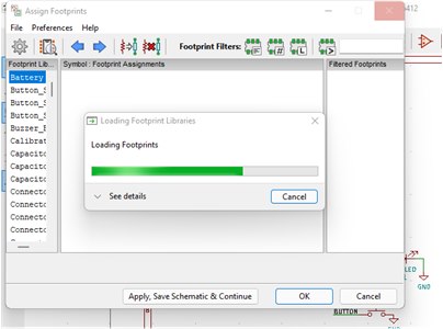
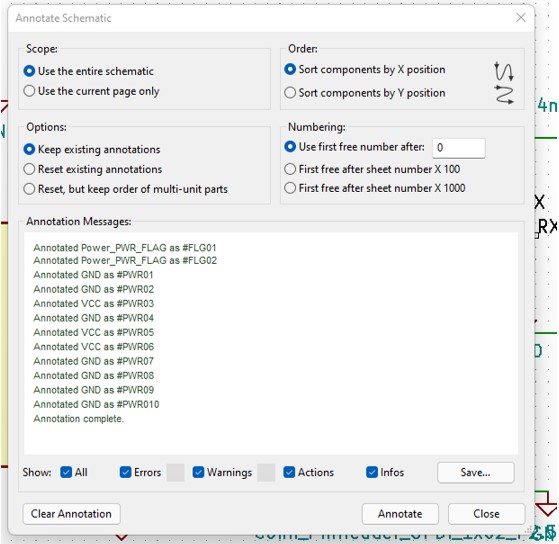
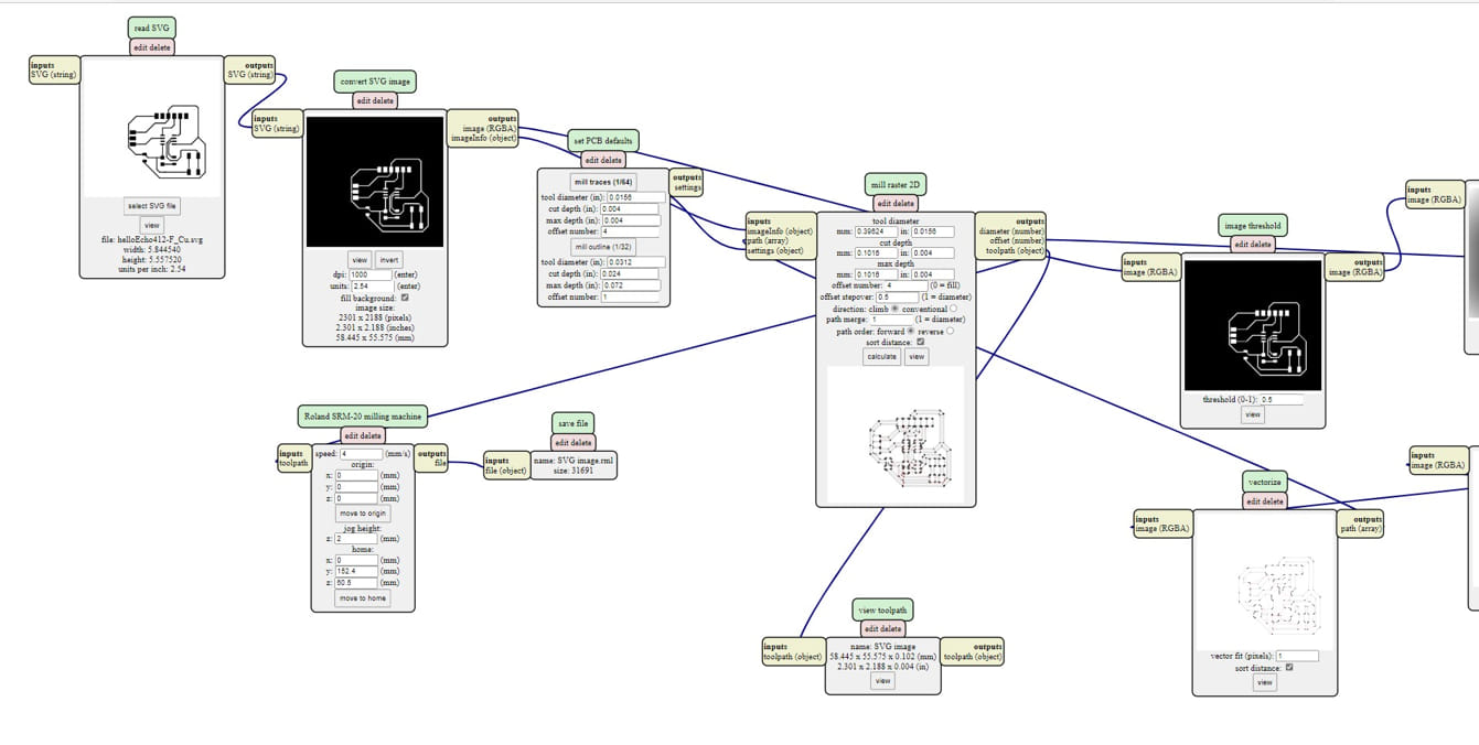
I used KiCad 5.1.12 and KiCad 6 to design our board. This software is open-source electronics design automation suite and collect several different programs (KiCad, Eschema, Pcbnew, Bitmap2Component, PCB calculator, and PI Editor) that work together to help in the design of a PCB.
KiCad can run on GNU/Linux, Apple macOS and Windows operating systems. You can find instructions and links to download the latest version of KiCad at http://www.kicad.org/download/.

From here you have access to eight tools: Eeschema, Schematic Library Editor, Pcbnew, PCB Footprint Editor, GerbView, Bitmap2Component, PCB Calculator and Pl Editor.
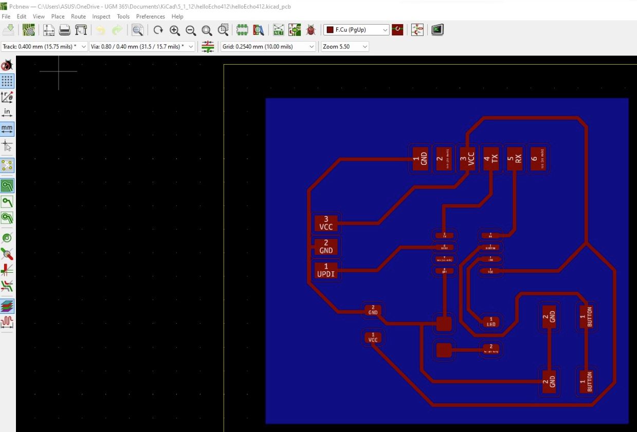
When the schematic has been drawn, the next step is to transfer the drawing to a PCB. Sometimes, we need to add a new component, a component needs to be changed to a different size, the net needs to be renamed, and so on.
‘Pcb layout editor’
-
Explained problems and how you fixed them, if you make a board and it doesn’t work; fix the board (with jumper wires etc) until it does work.
-
Included original design files (Eagle, KiCad, etc.)
- Soldering Process our Components on PCB
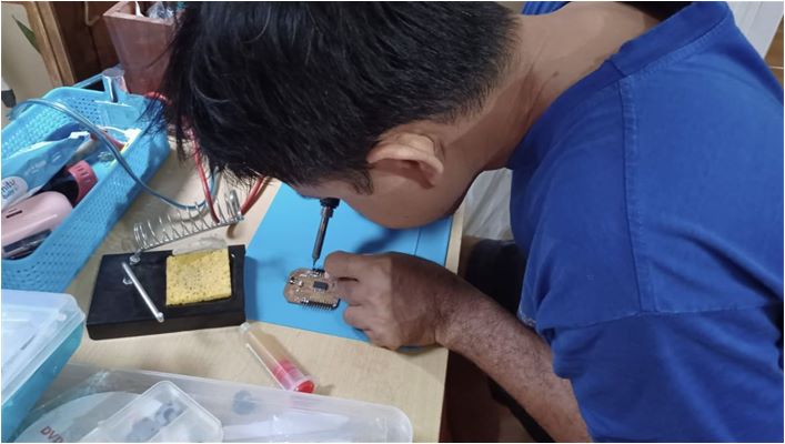
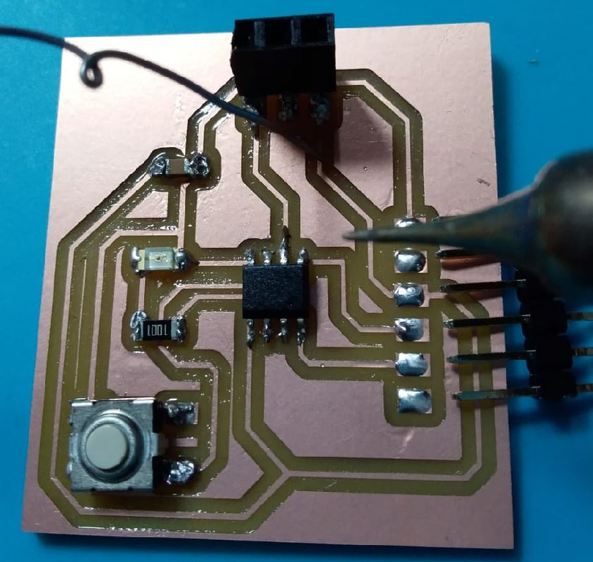
I found a lot of errors and connection mismatches after I checked with a digital multimeter, most of them happened because the soldering was not clean enough so that unexpected connections occurred between components with each other.
- Included a ‘hero shot’ of our board
- Loaded a program and tested if your board works
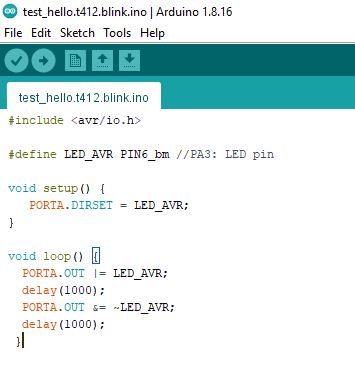
Loaded and tested for t412.blink.ino
Connecting and Loading
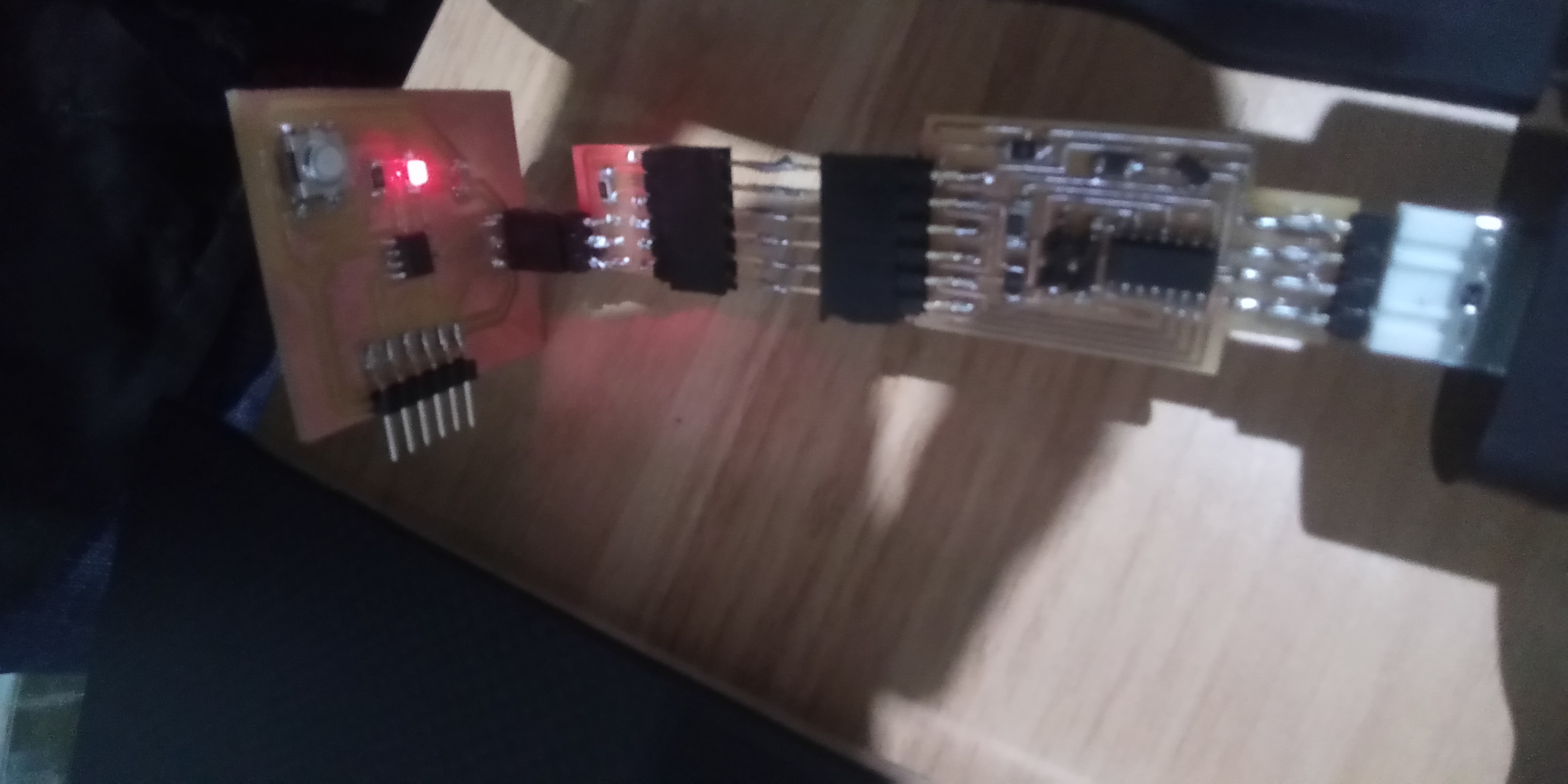
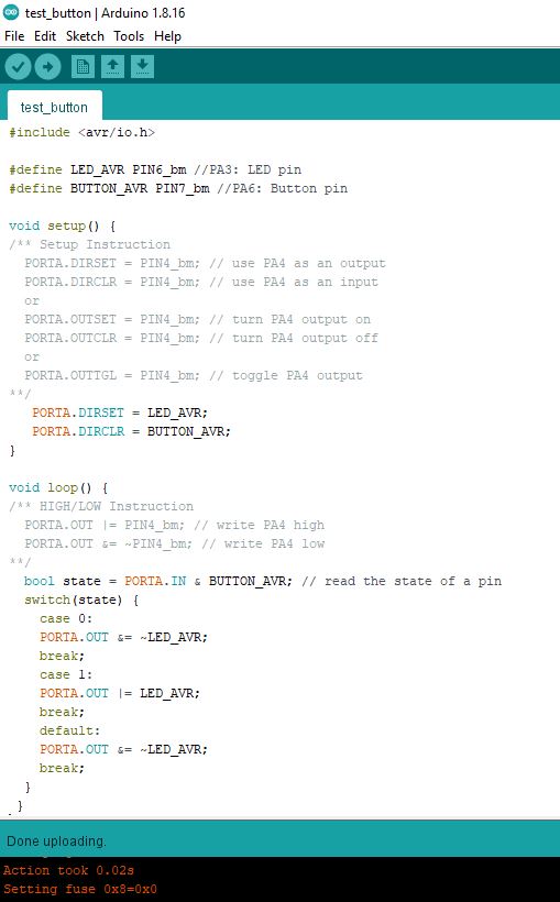
Loaded and tested for test button
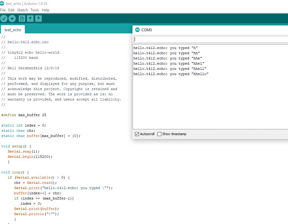
Loaded and tested for echo
LEARNING OUTCOMES
After conducted this assignment I got more information, knowledge, and experiences about how to:
-
Select and use software for circuit board design
-
Demonstrate workflows used in circuit board design.