4. ELECTRONIC PRODUCTION
# 4. ELECTRONIC PRODUCTION
Weekly Assigment Requirement
Group assignment:
- Characterize the design rules for our in-house PCB production process: document feeds, speeds, plunge rate, depth of cut (traces and outline) and tooling.
- Document our work (in a group or individually)
- Document our work to the group work page and reflect on your individual page what we learned.
Individual assignment:
- Make an in-circuit programmer that includes a microcontroller by milling and stuffing the PCB, test it to verify that it works.
The point that I have to answer
- Linked to the group assignment page
- Documented how we made (mill, stuff, solder) the board
- Documented that our board is functional
- Explained any problems and how we fixed them
- Included a ‘hero shot’ of our board.
Let’s get started! and show this week’s results
Group assignment
Milling Precision Test
For our group assignment we had to mill a test that would show the precision of our milling machine (Roland SRM 20). Both in terms of how thin of a line it can mill (with ample space along the sides to mill away), before it becomes so thin that it gets lifted off the yellow epoxy backing. And what the thinnest line is that it can mill between two close traces, giving us basically the diameter of the milling bit.
From the Fab Academy page for this week you can download the test traces and interior png files (the last entry in the CAM section).
Goal: Understand intimately the features and capabilities of your machine
- What are the machine’s technical specifications?
- What does the machine do?
- What are its key components?
- What are the machine’s limitations?
- How is the machine controlled?
- What file format can the machine understand?
- What cutting tools are available for the machine?
- What cutting tools are required for this assignment?
- Why are different tools needed?
- etc.
Every CNC machine…needs very specific settings to be defined…to properly cut specific materials with specific tools
Feed Rate >> lateral motion speed (it depends on hardness of material to cut, strength of cutting tool)
(Spindle) Speed >> rotation speed of the spindle head (described as RPM) and cutting tool (while working with this machine we have to avoid heat, and good chips can be used as indicator)
Plunge rate >> vertical motion speed ( it depends on material to cut, strength of cutting tool)
Depth of cut >> how deep to plunge into the material with each cut pass (it depends on “trace” vs “outline” cut…and characteristic of cutting tool>>strength, number of flutes)…typically, Depth of Cut = 1/2 endmill diameter
Kerf >> minimum width of cut, the material removed by the cutting tool depending on the diameter of the cutting tool (e.g. wider diameter tool, wider kerf…more space between trace lines)
For Group Assignment, I pushed in HERE.
Individual Assignment
Create the PCB board with SRM-20
Electronic production is one of the very important stages carried out at FabAcademy to support other electronics-based skills. The main activities in this assignment are electronic design and embedded programming.
-
Use CNC for cutting a circuit board.
-
We used FR1 type PCB stock material (which has a paper-based substrate under the copper which not a health hazzard and more gentle on the endmill) vs FR4 type (which has a fiberglass substate and the milled powder is hazzardous when breathed in and causes more wear and tear on the endmill).
-
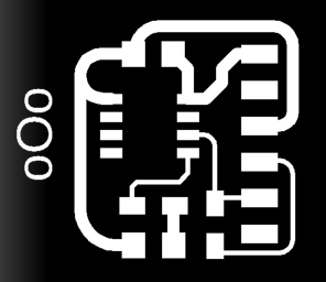
PCD design, in this assignment I produced FTDI USB-serial board. According to some references, future technology devices international Limited (FTDI) is serial communication through a USB port, and has a separate port for the TX and for the RX. I can’t program a new board with an FTDI, I use FTDI only for communicating from USB to serial.

- Preparing the machine and materials
Preparing

Preparing Machine
I have to turn on and connect the SRM 20 machine on the laptop to connect with the VPanel for SRM-20 software to determine the XYZ coordinate system of the milling area.
Using ‘mods’ mods
PCBs are prepared and cleaned to be affixed to the wood planks in the milling area. To tight-position on the wooden board, I used double-tape on the surface to make sure that during the milling process the position of the board did not change or shift. After the PCB is attached to the wooden board, the pressing process is carried out by placing a cleaning cloth on the top side to ensure that the PCB is firmly attached.
Next, the wooden board attached to the Roland SRM 20 metal board is tightened with the locking bolts on all four sides.
MODS Usage
Next I accessed MODs on mods.cba.mit.edu to find out the suitability of designing the .rml file and using the machine in the printing process.
In exporting RML file with mods, feed rate 4 mm/s is a default value, but plunge rate is not explicitly defined. I have to Open RML file with a text editor, and got PA; PA; VS4; !VZ4; !PZ0; 1200; !MC1; According to List of RML-1 instructions, VS: velocity select (feed rate for x and y axis), VZ: velocoty select (feed rate for z axis), which means plunge rate is 4 mm/s.
If I change the feed rate in mods, plunge rate will accordingly change. mods uses the same value for feed rate and plunge rate.
- After MODS appears, Right-click on the window, select Program -> Open Server Program -> select Roland SRM-20 machine type -> PCB png

- Also add save modules: Right-click -> Modules -> Open Server Modules -> Save files.

I have to make sure that the designs and jobs have to be saved with the correct names to call the files for milling.

- Connect the file in the mods module with the output file in the mods program, then create the trace of the path circuit board.

in the ‘mods’ view I saw the value of “dpi” or (dots per inc) and milling area.
For the mill tracess process I used a size (1/64) drill bit; tool diameter 0.0156 (in), cut depth 0.004 (in); max depth 0.004 (in) and offset number 4.
As for the mill outline, I used a drill bit (1/32) with a 0.0312 (in) tool diameter; 0.024 (in) cut depth, 0.072 (in) max depth; and 1 offset number.

- For next step, using Roland SRM 20, change the origin to be zero (x0, y0, z0)

-
Load the png file (select the linetest.png file) select the mill trace 1/64 click the calculate button, and then the mod will calculate and make the route automatically
-
The file (rml) downloaded and created path of route by clicked the view button sent to the SRM-20 Machine

Example milling process for interior using (1/32) of drill size.
- Loading design and cutting process

Processing time for milling trace have taken around 24 minutes and 16 minutes for interior.
- Inspecting and controlling the results

I used a soft brush and mask to clean the surface of the PCB from copper dust to identify the suitability of the milling results and make sure there was no damage to the designed circuit board.

Next, I removed and lift the milling results carefully using a spatula and adhesive remover to ensure that was perfectly clean the glue from surfaces.

Working for Electronic Production
- Soldering surface mount parts on a circuit

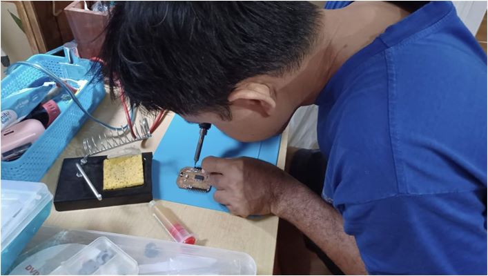
I soldered electronic components on my boards. Soldering electronic component type SMD is a big challenge for me. because besides I do not have basic knowledge of electronics skills, the very small size has a level of difficulty for me who has limited vision.


UPDI Programming (SAMD11C Burn-Bootloader)
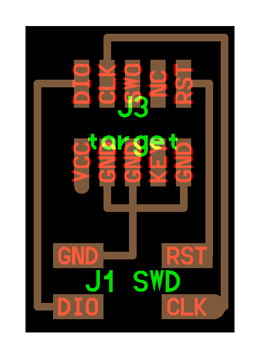
UPDI programming makes it possible for a single wire (connected to the microcontroller’s UPDI pin) to act both as a serial Transmission line (TX) and Receiver line (RX). The 4.9k ohm resistor contributes to this ‘switching’ ability. When a Programmer board(the program sender) is connected to a Target board (the program receiver) with a UPDI connection, only one of the boards needs to have the 4.9k ohm resistor connected on the UPDI line.
I worked together with Jans and Setyawan, my colleagues in FabAcademy 2022, and they help to get the programming working.
To program my board I had to understand how the UPDI adapter, my PCB board and FTDI work. FTDI (Future Technology Devices International) is used to establish communication with your board/MCU via my computer. FTDI has the ability to talk to the PCB board via VCC, GND, TXD (Transmit), and RXD (Receive) connections.

While UPDI (Unified Programming and Debug Interface) is used to program the board. Three sockets allow programming and powering my board.
 ,
,
- Write program on the SAMD11C
I used Atmel-ICE, as a powerful development tool for debugging and programming ARM® Cortex®-M based SAM and AVR microcontrollers with on-chip debug capability.

Following the directions of the Kamakura instructor, I created a document assignment.

The first thing to do is to mark the end of the jumper/dupont cable that is used to anticipate installation errors.
I used a pin compatibility jumper cable to connect the FTDI to UPDI adapter for VCC, GND, TXD, and RXD to FTDI with VCC, GND, TXD, and RXD to UPDI.

Checking the connection on each connected cable and whether or not additional resistors are needed in the connection.
Once these three are connected, we can program the PCB. Below is a diagram of how the communication will occur between the FTDI to the UPDI to the PCB.
- Debug
In my board, it already has a 4.9k ohm resistor on its UPDI line…therefore, I would not need the 4.9k Ohm resistor on our USB-D11C-FTDI programmer. Instead…solder a 0 ohm resistor in its place.
From Jun san’s documetation

windows also recognized particle debugger automatically, but couldn’t burn a bootloader.
In mods, plunge speed was equal to feed rate. Check a generated RML file.

-
found that error caused by 4 pin were incorrect mounted locations.
-
In the programmer board. I did experiment what if change the position of 2 neigboor, what error would come up. I did that for all.
-
When The board was unrecognized I checked the usb port connection.
Then I burned a bootloader to enables our board to work with an Arduino sketch. The bootloader used to the ‘edbg’ to burn to D11C and Edbg can download in https://taradov.com/bin/edbg/, then ran this command.
edbg-windows-r29.exe -bpv -e -t samd11 -f sam_ba_Generic_D11C14A_SAMD11C14A.bin
I got error when connected it to a USB (in my computer; “USB not recognized”). I found the cause that happened due to unconnected problem. I added a USB male connector to solve it.
Check the Connection
Then I checked my results to identify bad or bad or failed connection with multimeter.

and this is the result…when soldering components on to your USB-Samd11C-FTDI programmer; hold off to solder the 4.9k Ω resistor.
 .
.
How-to’s are below!
 .
.
Flow Process for Individual Assignment
This week, I completed the group assignment with Setyawan and Jans at Field Research Center (FRC) UGM and conducted some activities:
-
Windows automatically install driver when I connect Atmel-ICE
-
Downloaded edbg binary from https://taradov.com/bin/edbg/
-
Tried “edbg-windows-r29.exe -h” and terminal will return some messages download sam_ba_Generic_D11C14A_SAMD11C14A.bin from https://github.com/mattairtech/ArduinoCore-samd/blob/master/bootloaders/zero/binaries/sam_ba_Generic_D11C14A_SAMD11C14A.bin
-
Connected Atmel-ICE and USB-D11C-serial via squid cable.
-
Typed in Terminal(command prompt) to burn a bootloader “edbg-windows-r29.exe -bpv -e -t samd11 -f sam_ba_Generic_D11C14A_SAMD11C14A.bin” Now the board is ready for working with an arduino sketch.

- In Arduino IDE, we installed core (MattaireTech SAM D|L|C core, megaTinyCore) from Board Manager, and select D11C board
- Uploaded SAMD11C_serial.ino

-
Downloaded hello.t412.blink.ino
-
connected USB-D11C-serial with hello.t412.blink board

-
In Arduino IDE, selected 412 board, serialUPDI programmer and others
-
Uploaded the sketch

- Checked the LED blinking
Learning outcomes
After joined Prof.Neil Course and conducted assigment we were able to: 1. Described the process of milling, stuffing, de-bugging and programming 2. Demonstrate correct workflows and identify areas for improvement if required
What we have to answer in this session
-
I have to be more thorough and careful in operating the machine according to the instructions. Steps that seem trivial and simple can sometimes be very important.
-
I have to check every component and equipment such as at the PCB milling and soldering stage to see if it is installed firmly enough.
-
Occupational safety and health is very important at every stage to protect ourselves and our environment (tools, materials, etc.)
Important Files
Links As Importance References
-
http://academy.cba.mit.edu/classes/embedded_programming/SWD/hello.SWD.10-4.1.png
-
https://www.rolanddg.eu/en/products/3d/srm-20-small-milling-machine/features