7. Electronics design
For this week I started my experience with kiCad and at first was like a new whole world opening in front of my eyes and almost a nightmare the fist proves I made, until I got a little bit used to the work flow.
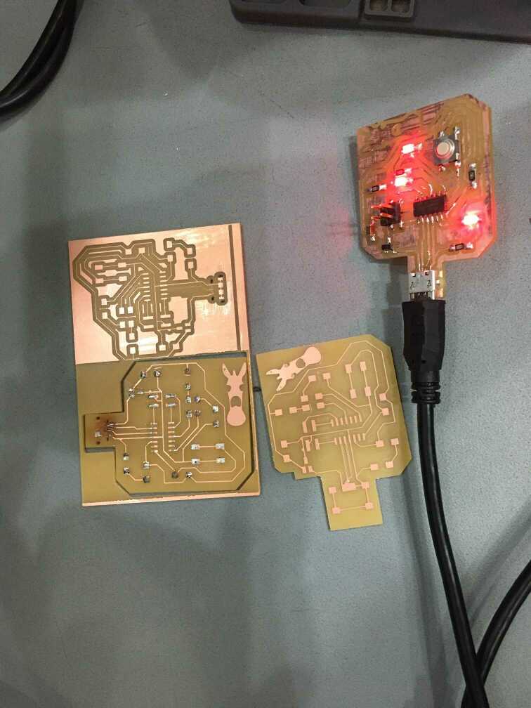
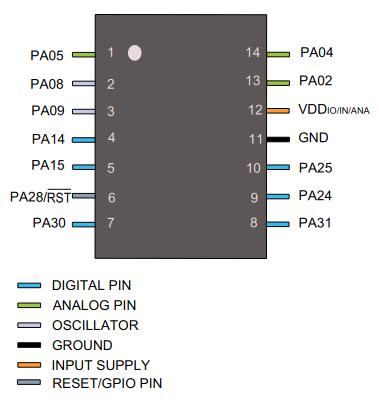
I decided to make a simple board with a button and two led using the ATSAMD11C14A
Designing the board
Setup KiCad
To desing this board I have been doing and undoing for three days until I got something usefull.
the first issue I found was that the version of kiCad I wa using wasn’t compatible with some of the footprints of the lab library we download, to make this work together I had to download the last version of kiCad to be able to see all the footprints. With the kiCad 6.0 almost everyting was OK.
To load the libraries in kiCad open the program and at the menu that apears on the top where it apears Preferences and there are two places where you have to load two files.
- Manage Symbol Libraries
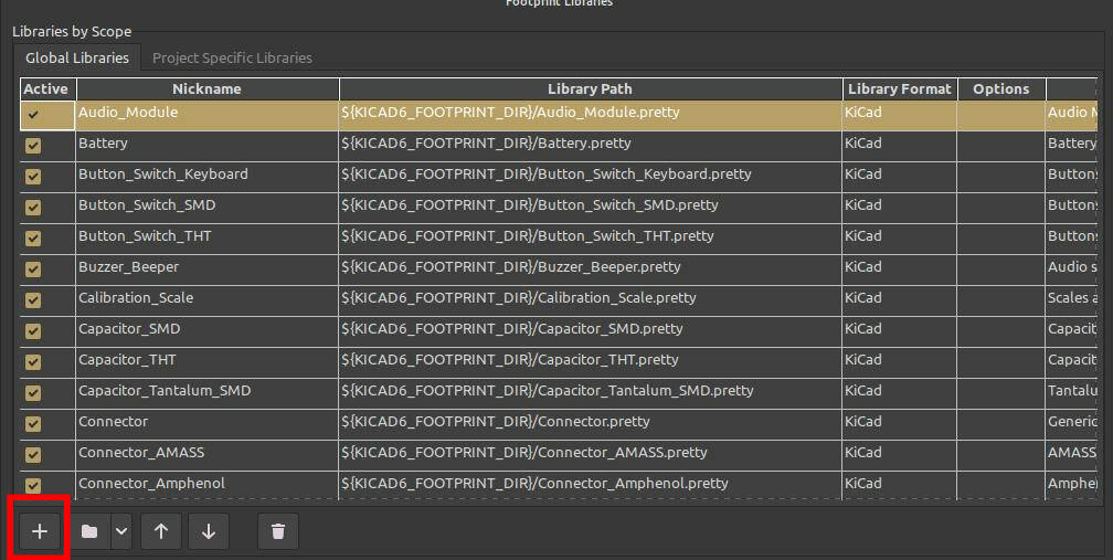
- Manage Footprint Libraries
In both cases a new window apears and in the bottom left part a symbol “+” lets you serch for the file you want to charge. In the symbol librariescharge the .lib file, in the footprint libraries charge the folder .pretty.
Start designing
To desing a PCB you will need to maje two files.
the first one is the schematic that its an easy schema where you have to make a first aproach with all the components you are going to use and how are going to be connected with some labels.
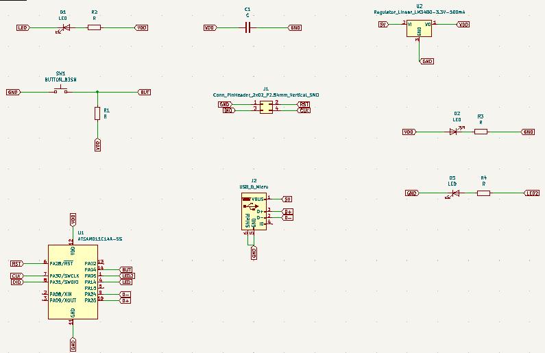
This is the easy part where you can se more or less how it’s going to be everithing connected.
Now it’s time to make the make all the paths. This has been a puzzle dificuld to solve, try to connect all the elements without crossing paths and trying to make a small board.
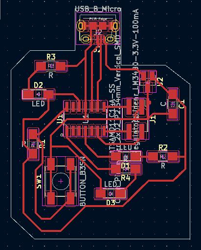
I have made a line in white arround the paths to define the outline of the PCB and not having to do it in Inksape, I left a little bit of space in the lower part to put an small drawing.
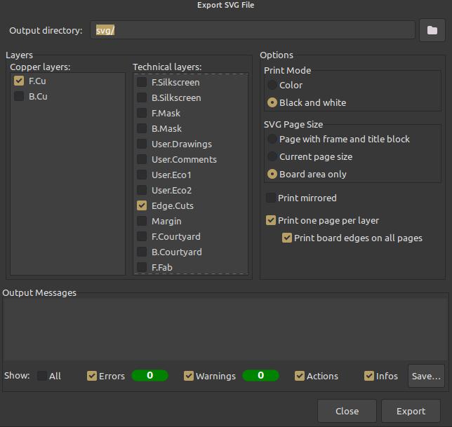
To export the .svg images go to files export .SVG, a new window will open and in my case I want to export two layers, the one with the traces (F.Cu) and the other one with the ouline (Edge.Cuts). the first onexport_svgeis in the Copper Layers block and the Edge.Cuts is in the Technical layers select both.
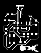
Afer opening the files in Inkscape I realized that some of the paths were very thick and the space left between wasn’t enough to make the end mill pass through. I ended up making some black squeres and putting them on top to hide the paths under. Finaly export the diferent images in .png and remember to put the quality to 1000 dpi.
In this case I have made 3 files
- Traces
- Holes
- Outline
Tgere three molds are going to be cutted in this order the first one with the 1/64 inches end mill and the last two with the 1/64 inces end mill.


Cutting the PCB
I have print not one PCB the second one wasn’t good not even the third one, the forth PCB I cut was the good one. Until I got the good PCB i modified the Inkscape files lots of times until I got the good traces in the mods, because at first the end mill wasn’t capable to pas between some traces.
I also tried to lie to the CNC to make it believe that the end mill was thinner so it can go inside the small gaps but end up cutting all the traces really thin and those poeped out of the board.