5. Electronics production
TO GENERATE PCBs!!!
modsproject.org
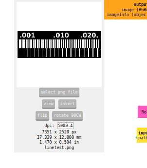
“.png” or “.svg” files (always black and white) better to use “.png” always use at least two files one for the circuit path and another one for the outline cut, if need holes use a third file for the drill. always export in 1000 dpi to get good quality image ¡check size of the image! if not the origin may change and the PCB will be destroyed.
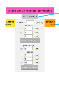
open program srm-20 mill absolute position
open program set up (viual scripting nodes)
select png or svg files black part is the part that the machine is going to mill white part is the one the machine is going to keep
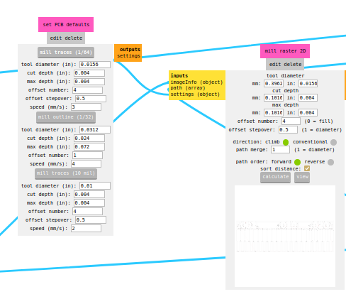
define settings (set pcb defaults) select de tool that is going to be used will change settings in (mill raster 2D)
important to de the Z correctly to not break the tool if goes to deep
important to do the Z correctly to not cut less material than desired
-
ofset number –> number of times that the tool is going to pass arround the path if = 0 cleans all the copper that is not going to be used
-
offset stepover –> 0.5 overlaping the tool of the previous path
-
direction –> use climb
-
view –> pre visualize tha paths check the path is correct and is not leaving two components together
-
speed –> 3 for path cutting // 1.5 for outline cutting
-
origin –> 0,0,0
-
jog height –> distance the tool is moving when not cutting DON’T GO TO LOW!
-
home –> 0,0,10 remeber to change the Z value to not scratch the PCB when finish
¡CONNECT THE OUTPUT TO THE SAVE FILE!
OUTLINE CUT
- origin –> lower left corner
- offset –> 1
- speed –> 1.5
- depth cut –> 0.6
- total depth –> 1.75
PATH CUT
- origin –> lower left corner
- offset –> 4
- speed –> 3
- depth cut –> 0.1
- total depth –> 0.1
PROGRAMMERS
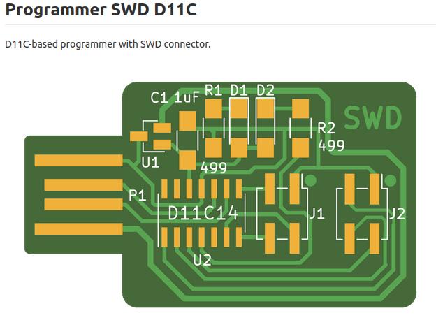
To burn the bootloader to other microcontrollers
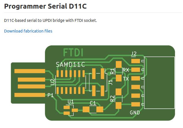
To program microcontrollers that does not talk usb natively
—
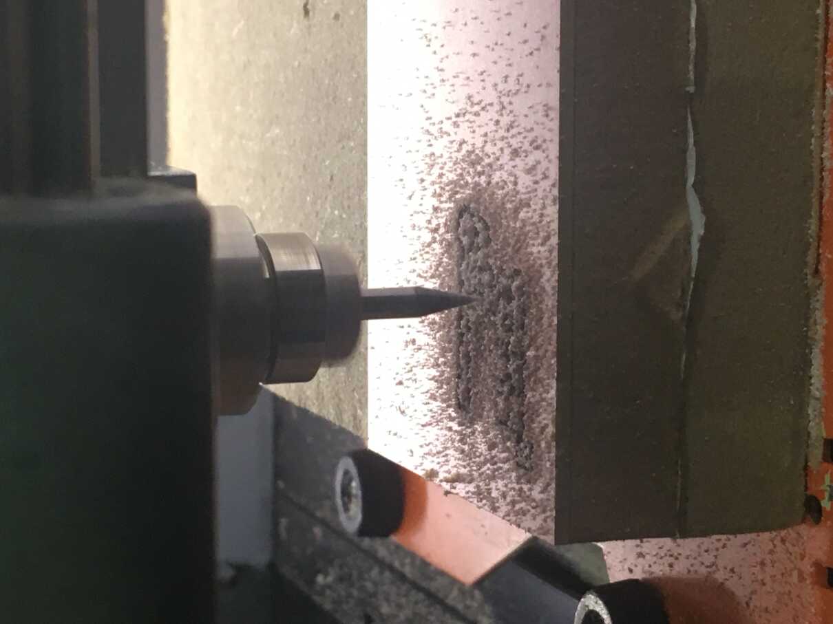
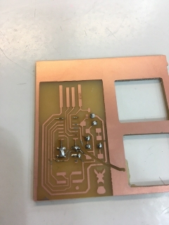
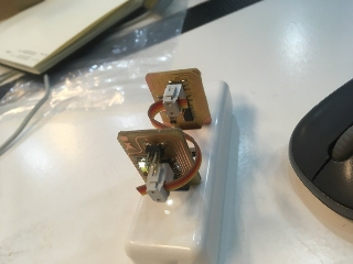
This is the first try failed of the swd-D11C programmer.
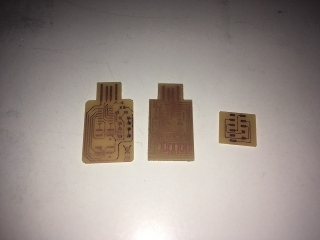
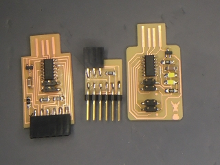
This are tha final PCB
To clean the copper of the PCB I run two times the traces file, one time with the 1/64 end mill with an offset of 4 lines and then, I run the same file with the 1/32 end mill with an offset of 0 in orther to clean all the copper and at the end cut the outline.
And finaly just solder the PCB with all the components.
Programing SWD D11C
In order to install edbg in linux I need some dependences.
To libudev-dev in Ubuntu
sudo apt-get update -y
sudo apt-get install -y libudev-dev
Then I can install edbg to my computer to do it i have to clone the repository from gitlab.
Once I had the repository I open the folder in terminal and make all.
to run binary files in linux you have to add ./file_name so remember to add it every time.
Finaly the last step is to program the programmer so I need a pcb allready programmed and conect each other.
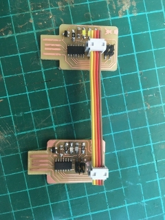
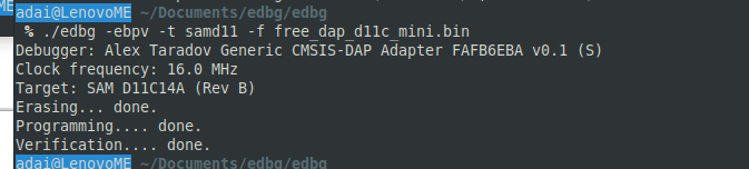
And then connect both to the computer and run ./edbg -ebpv -t samd11 -f free_dap_d11c_mini.bin
one last thing to remember is to copy the “free_dap_d11c_mini.bin” file i the same folder tha the edbg program.
The whole week to get this message.