5. Electronics production
This week, I will create an AVR ISP programmer.
As a beginner, I did not really know what to do , so I have followed the tutorial about the ISP from the fabacademy.
First question : what is ISP ???
ISP stands for In-System-Programmer. You need this small circuitboard to program a chip that is already fixed to a circuitboard-system. Invented to make the workflow(1) easier for a factory so you can first make the system and then program the chip. ( Earlier, companies needed to buy already programmaned chips). Re-writable EEPROMs(2) came out, the ISP became the standard to re-program the chips. Any Arduino board has its own ISP. We are going to isolate the ISP on a board and be able to program different boards within it.
Translated words for Dummies :
(1)What is a workflow? :
From IBM: A workflow is a a system for managing repetitive processes and tasks which occurs in a particular order. They are the mecanism by which people and enterprises accomplish their work, whether manufacturing a product, providing a service, processing information or any other value-generating activity.
(2)What is EEPROM ?
From wikipedia : EEPROM (also E2PROM) stands for electrically erasable programmable read-only memory and is a type of non-volatile memory(3) used in computers, integrated in microcontrollers for smart cards and remote keyless systems, and other electronic devices to store relatively small amounts of data by allowing individual bytes to be erased and reprogrammed.
(3) what is Non-volatile memory?
From wiki: Non-volatile memory (NVM) or non-volatile storage is a type of computer memory(4) that can retain stored information even after power is removed. In contrast, volatile memory needs constant power in order to retain data.
(4)what is computer memory?
_From wiki: In computing, memory is a device or system that is used to store information for immediate use in a computer or related computer hardware and digital electronic devices.[1] The term memory is often synonymous with the term primary storage or main memory. An archaic synonym for memory is store.[2] Computer memory operates at a high speed compared to storage that is slower but less expensive and higher in capacity. Besides storing opened programs, computer memory serves as disk cache and write buffer to improve both reading and writing performance. Operating systems borrow RAM capacity for caching so long as not needed by running software.[3] If needed, contents of the computer memory can be transferred to storage; a common way of doing this is through a memory management technique called virtual memory. Modern memory is implemented as semiconductor memory,[4][5] where data is stored within memory cells built from MOS transistors and other components on an integrated circuit.[6] There are two main kinds of semiconductor memory, volatile and non-volatile. Examples of non-volatile memory are flash memory and ROM, PROM, EPROM and EEPROM memory. Examples of volatile memory are dynamic random-access memory (DRAM) used for primary storage, and static random-access memory (SRAM) used for CPU cache. Most semiconductor memory is organized into memory cells each storing one bit (0 or 1). Flash memory organizationincludes both one bit per memory cell and multi-level cell capable of storing multiple bits per cell. The memory cells are grouped into words of fixed word length, for example, 1, 2, 4, 8, 16, 32, 64 or 128 bits. Each word can be accessed by a binary address of N bits, making it possible to store 2N words in the memory.
In order to program most powerfull board form the project, we will need to understand another definitions:
FTDI and UPDI :
The Unified program and Debug Interface (UPDI) is an proprietary interface for external programming and on-chip debugging of a device. UPDI is used for the newer generation ATTINY’s Microcontroller (MCU). UPDI uses only 2 pins via USB serial communication. Combined UPDI and FTDI. FTDI is a communication protocole for serial communication, very popular.
What is MCU ?
From ressources.pcb An MCU is an intelligent semiconductor IC that consists of a processor unit, memory modules, communication interface and peripherals. The MCU is used across a broad range of applications, including washing machines, robots, drones , radio and game controllers.
Getting back on the ISP programmer :
Summary from Fabacademy: « The FabTinyStar is yet another version of an AVR ISP programmer/board that can be produced in a fab lab using a milled PCB and readily available components. The project is based on the efforts of many people. For more history of the FabTinyStar and the people who have contributed to it, please refer to Zaerc’s FabTinyStar page. »
Tutorial here : http://pub.fabcloud.io/tutorials/week04_electronic_production/fabtinyisp_english.html
components :
There are small and they need to be well organized.
| nb | specifications |
|---|---|
| 1 | 1x ATtiny45 or ATtiny85 |
| 2 | 1kΩ resistors |
| 2 | 499Ω resistors |
| 2 | 49Ω resistors |
| 2 | 3.3v zener diodes |
| 1 | red LED |
| 1 | green LED |
| 1 | 100nF capacitor |
| 1 | 2x3 pin header |
built-in procedure:
_from fabacademy:
The LEDs and their associated resistors are optional; the red LED lights when the target circuit is powered, and the green LED lights when the programmer is talking to the target. Solder the parts to the PCB, using the schematic and board image below as a reference for component values and placement. Start with the most difficult parts (the ATtiny45) first, so you have the most access. Install the ISP header last, as it is large and can get in your way if you do it earlier.
Bridge :
Use solder to create a bridge on the jumper near the ISP header (J1). This temporarily connects VCC to the Vprog pin on the ISP header so that the header can be used to program the tiny45. (The programmee supplies voltage on this pin and the programmer detects it). Once it’s programmed, we’ll remove this bridge to turn the board into the programmer rather than the programmee.
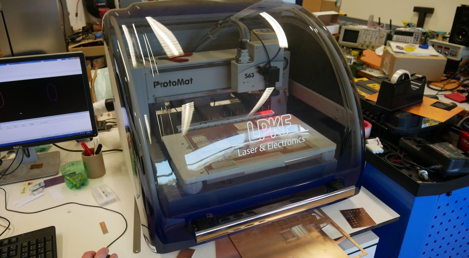
Milling machine : LPKF – Protomat – S63
My engineering school has an expensive milling machine.
 Part no. 127411
| parameters | specifications |
|---|---|
| Max. material size and layout area (X/Y/Z) | 229 mm x 305 mm x 35/22 mm (9” x 12” x 1.4/0.9”)* |
| Resolution (X/Y) | 0.5 μm (0.02 mil) |
| Repeatability | ± 0.001 mm (± 0.04 mil) |
| Precision of front-to-back alignment | ± 0.02 mm (± 0.8 mil) |
| Milling spindle | Max. 60,000 rpm, software controlled |
| Tool change Automatic, 15 positions | |
| Milling width | adjustment Automatic |
| Tool holder | 3.175 mm (1/8”) |
| Drilling speed | 120 strokes/min |
| Travel speed | (X/Y) Max. 150 mm/s (6”/s) |
| X/Y-drive | 3-phase stepper motor |
| Z-drive | 2-phase stepper motor |
| Dimensions (W x H x D) | 670 mm x 540 mm x 840 mm (26.4” x 21.3” x 33” |
Up to 15 tools are automatically changed during production.
The 60,000 rpm milling spindle ensures the shortest machining times and highest accuracy.
There is a dust extraction and a vacuum table.
-
The device is very precise. Dust extraction Vacuum table. There is a dedicated software very easy to use.
-
Very expensive. -too complex for a beginner.
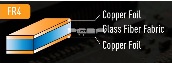
What is FR4 circuit board ?
To sum-up: FR-4 (or FR4) is a NEMA grade designation for glass-reinforced epoxy laminate material. FR-4 is a composite material composed of woven fiberglass cloth with an epoxy resin binder that is flame resistant (self-extinguishing).
From https://www.pcbastore.com/blogs/fr4-circuit-board.html
Many electrical professionals and people dealing with electronic devices know the value of printed circuit boards (PCBs). These boards have transitioned traditional electronic devices to be simpler, high-quality, and enhanced their performance. In other words, PCBs have played an integral part in many electronic circuits and devices for a long time. Besides, electronic engineers also contemplate various materials employed in developing these boards. One such critical material is the FR4. FR4 is undeniably the ground or the backbone material popularly utilized in creating PCB boards.
Unfortunately, not everyone is aware of what FR4 entails, especially individuals with no prior experience. Therefore, this article seeks to give an insight into what FR4 circuit board entails, why it is a commonly used PCB base, why consider using it, and when to avoid utilizing the material.
The FR4 circuit board is the standard name employed in PCB manufacturing. FR is the abbreviation of flame retardant. The value 4 is perceived as the typical rating of the material. The name FR4 is primarily employed in glass epoxy laminated sheets. This is something that appears to be woven and thin cloth sheets.
Basically, the FR4 circuit board is popularly considered to be a composite structure. Its fiberglass composition plays a critical part in providing the FR4 its essential structural stability. The fiberglass layer is based on the inner side, where it is bound and surrounded by epoxy resin that can resist flame. Epoxy resin is essential as it provides FR4 material the suitable rigidity.
Since FR4 works as the backbone of PCB, it is crucial to select the right FR4 material. Some of the available options include:
Standard FR4

FR4 High IRC

FR4 High TG

FR4 no copper
While choosing FR4 circuit board material, there are some aspects that you must keep in mind. One such aspect is the FR4 board thickness measured in inches, thousand, or millimeters.
Usually, the suitable FR4 material must be thin to help develop a PCB board with limited space. The reason to consider thin material is that it can accommodate many fragile components needed to create devices like USB connectors, Bluetooth devices, and other items using PCB boards. Thin FR4 material is yet ideal for creating larger devices where space-saving design is required.
Alternatively, thin FR4 material is best applied in flexible devices. For example, employing a thin FR4 material for medical and automotive PCB boards is appropriate since these boards demand consistent flexing.
Consequently, avoid selecting thin FR4 because it can initiate a higher risk of board fracture or damage.
Furthermore, the thickness of the FR4 material can influence the weight of PCB as well as the compatibility of the components.
We use 35microns FR4 board. The copper layer is 35 microns.
Fabacademy tests.
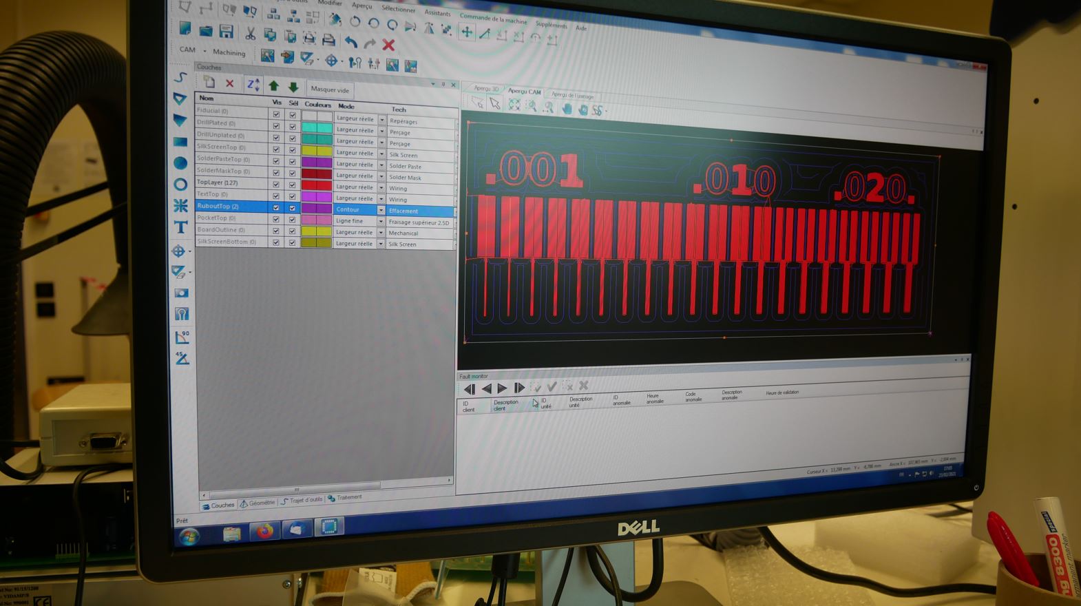
Using the fabacademy template in order to know the accurancy and finest tool paths.
Conclusions
One issue was the text on the board, I have created one svg file to get the text properly. It sounds easy to use a simplest machine such as the 3018 cnc. I will try it when I go to la Machinerie. A lot of things are automated so you do not have to take care about anything. The price is too high to let students alone on the machine…And it looks like an “apple” products, you do not really set everything.
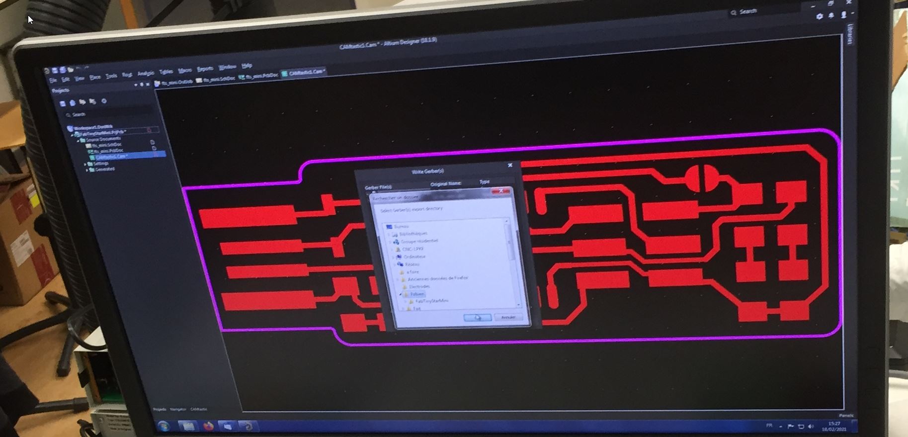
Files from Altium.
After downloading the Altium software, I have opened the files from the fabacademy in order to get the gerber files.
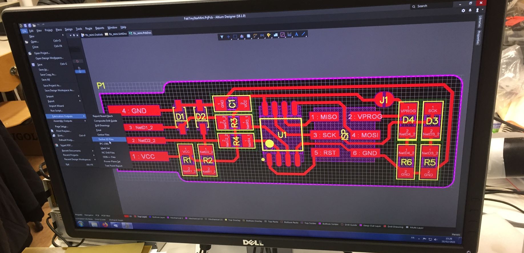 I have exported two files: mechanichal1 and top layers.
 One file for the inner trace, and a second one for the outer trace.
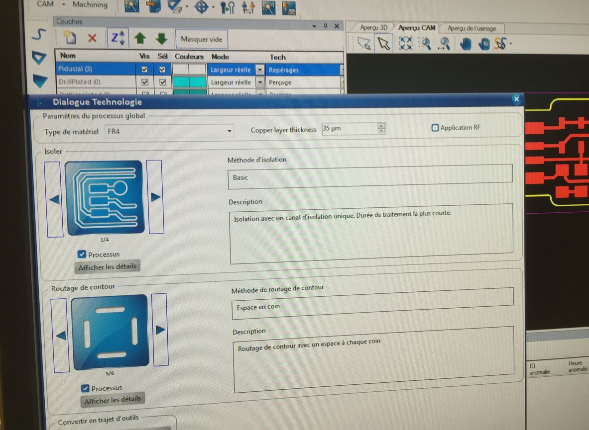
material
FR4, one-sided copper, 35 microns,1.6mm thick material
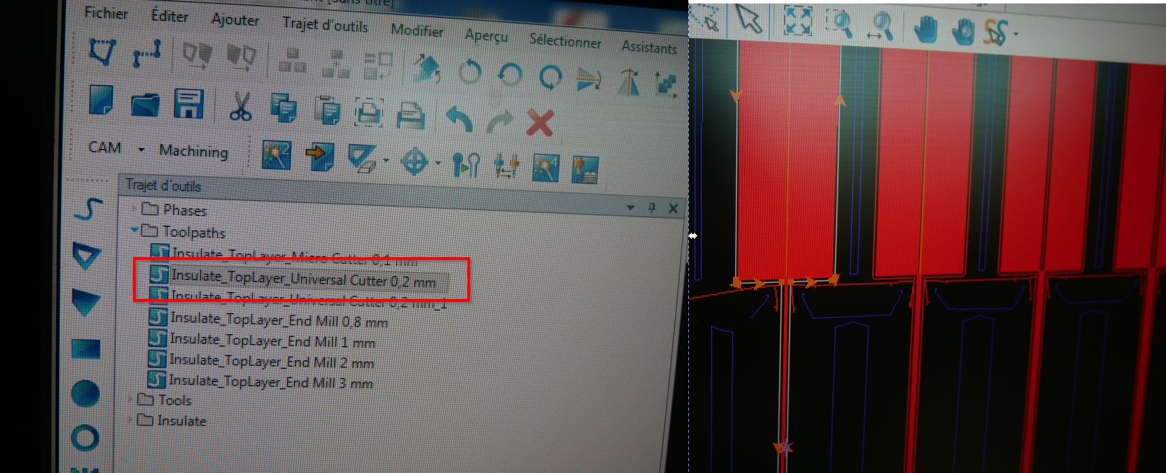
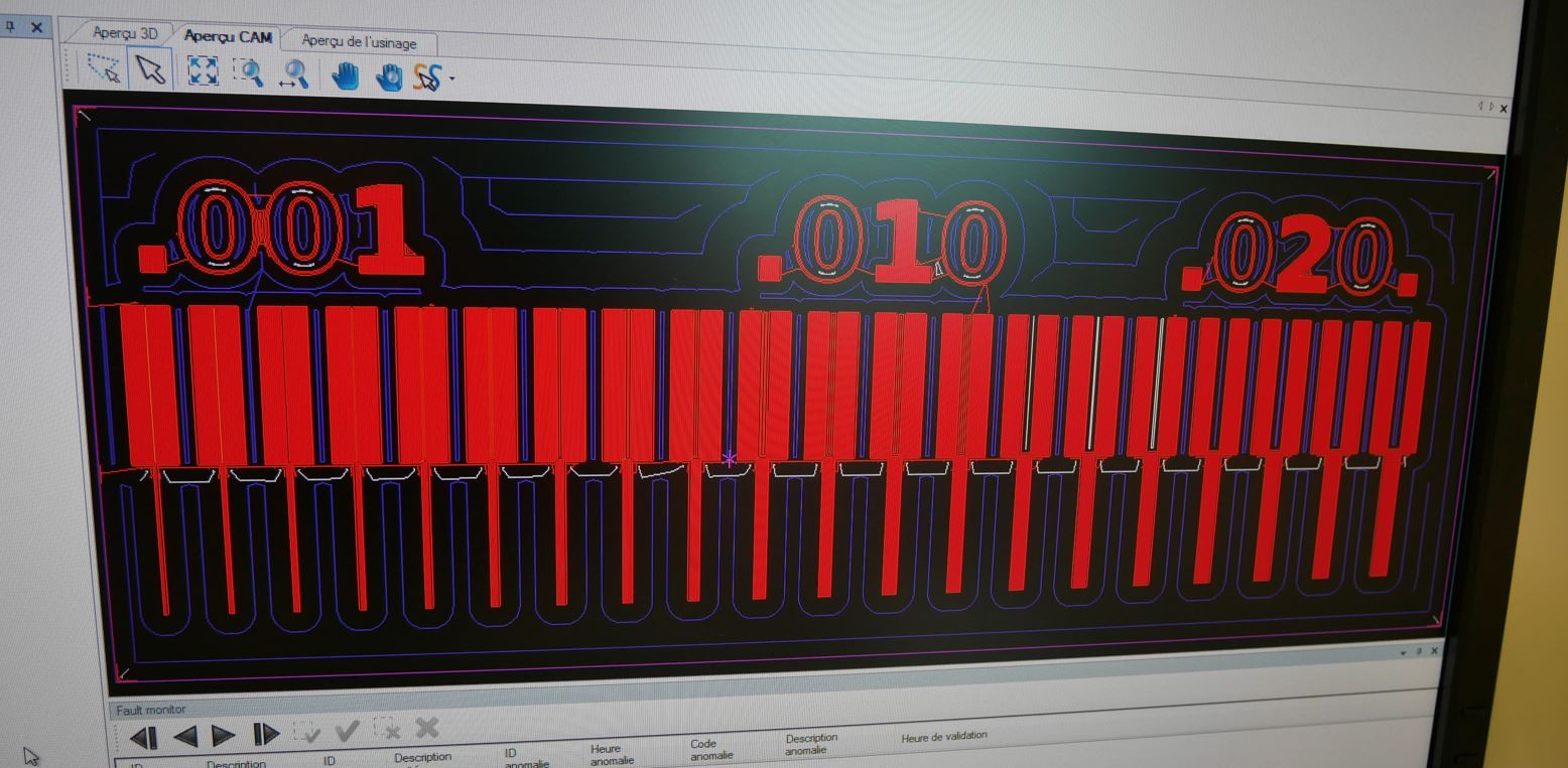
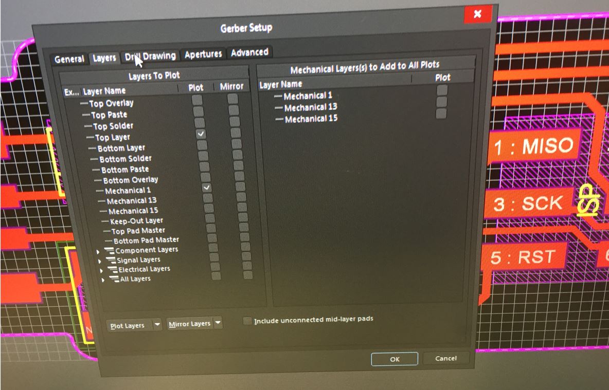
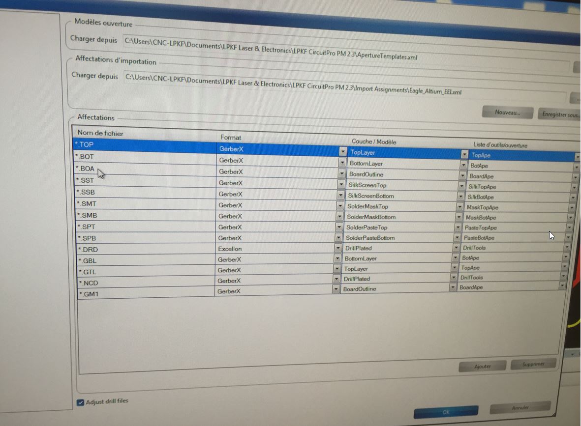
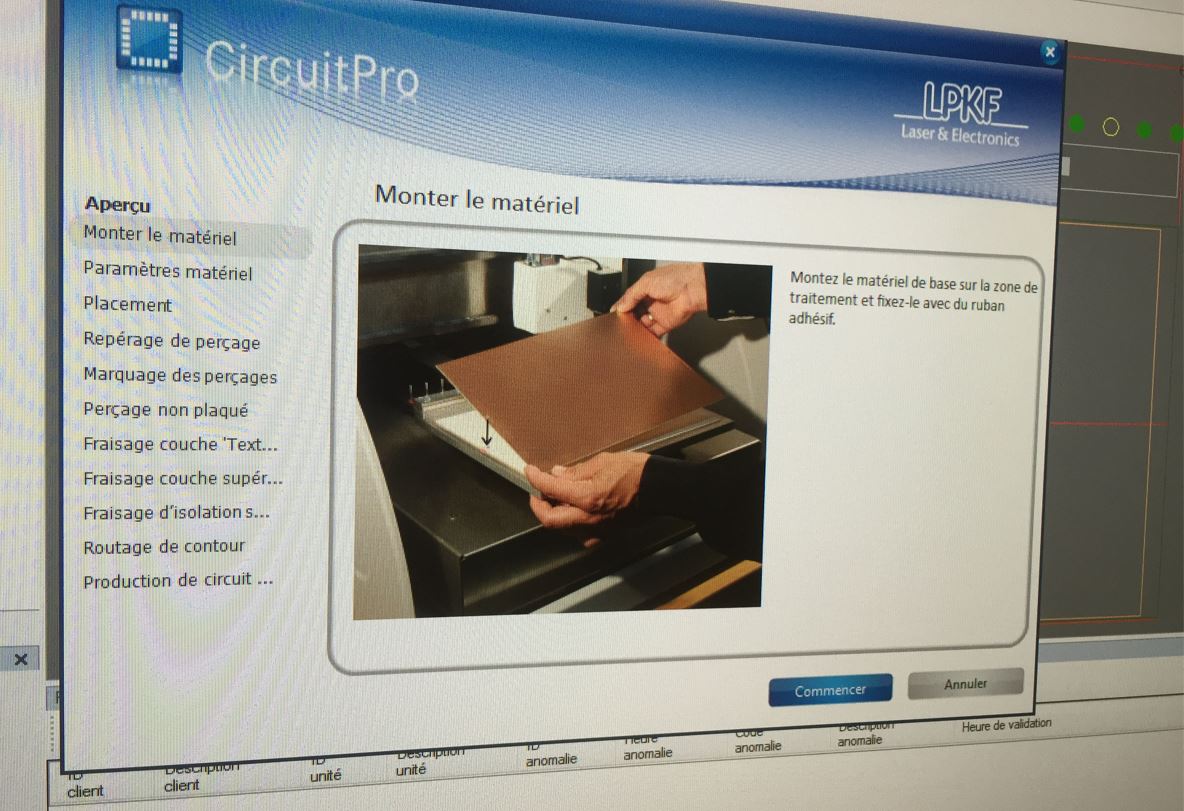
Open gerber files:
You can open the gerber files after exporting from altium. ( the top layer and the mechanichal layer)
You have different options for milling, You can keep the cupper. It lets just 0.2mm offesting. to the total insulation. .
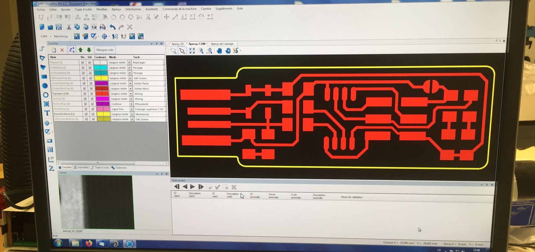
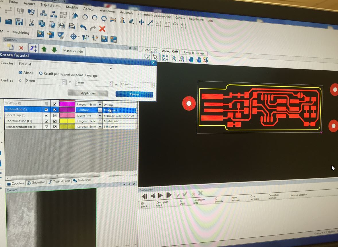
The software has a program to detect exactly the position of the current job. You have to mesure/mark 3 dots on your board.You get the camera option on the software. You can move the camera very precisely where you marked your board.
First milling the space between traces, next routing the main board.
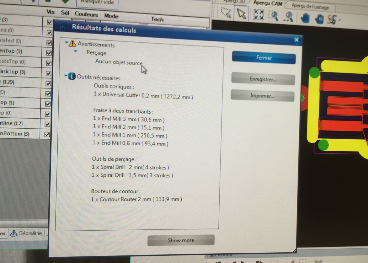
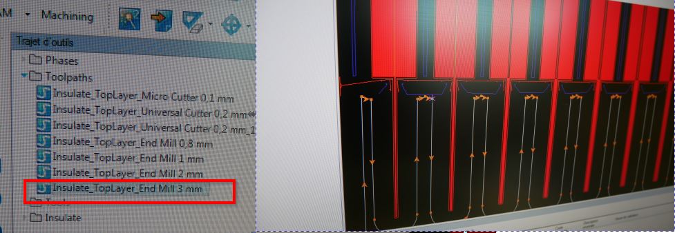
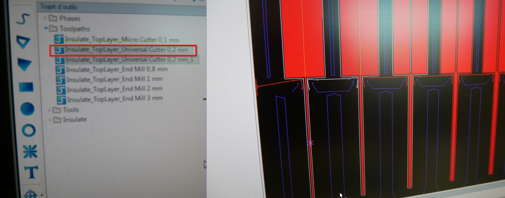
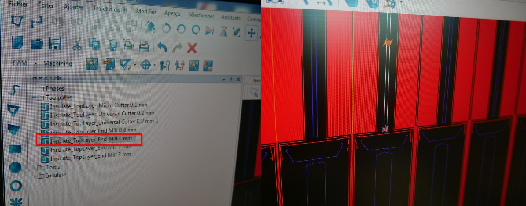
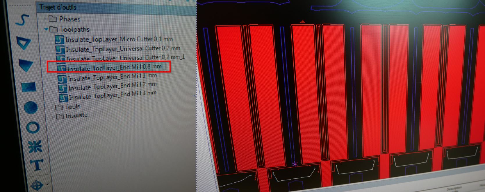
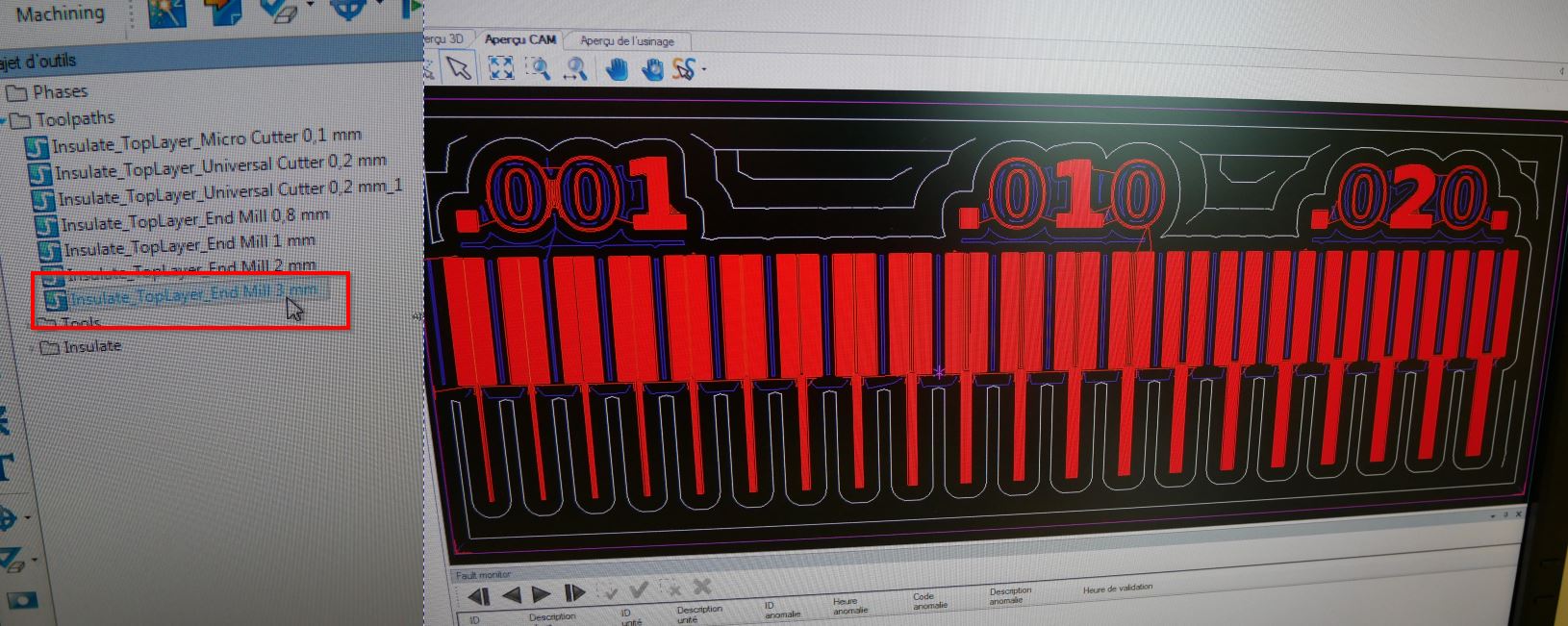
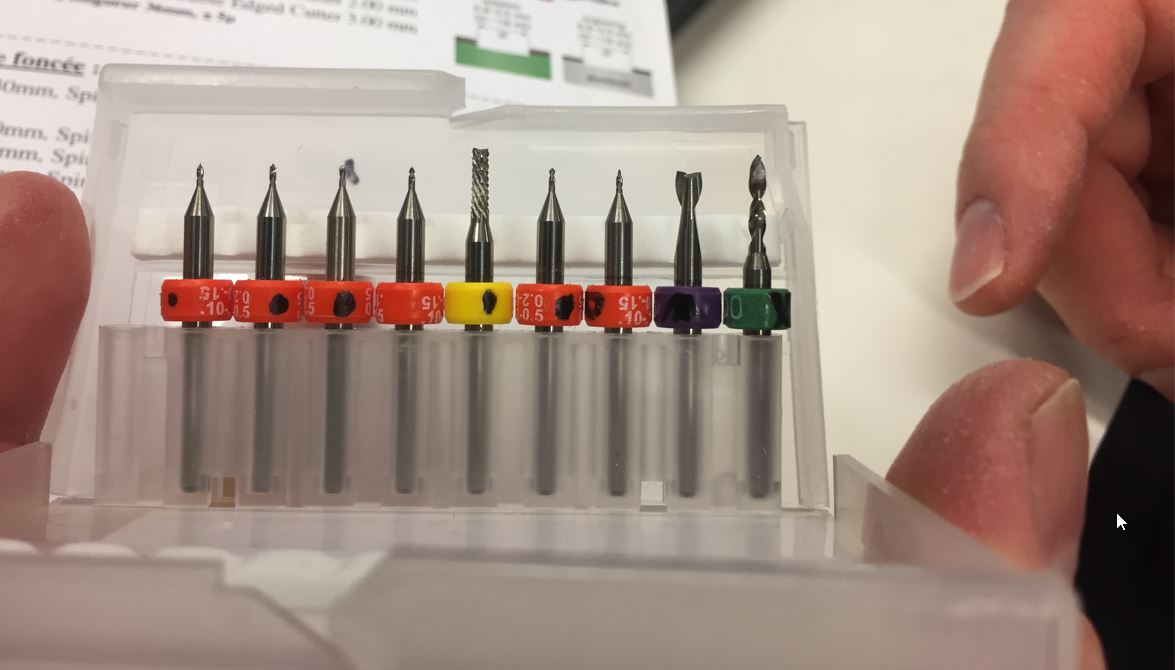
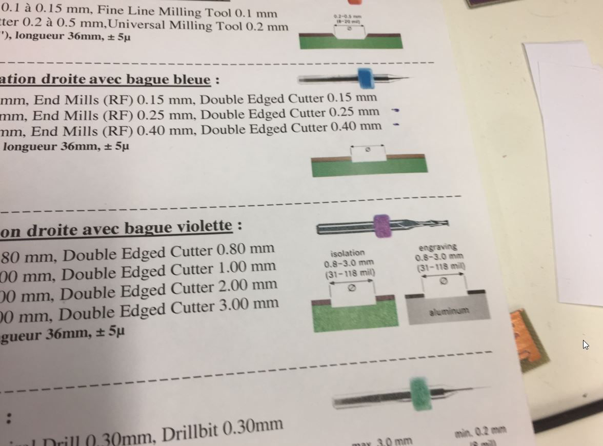
milling tools:
We will use different milling bits: There are flat tools but also V bits. The V bites allow us to have thin and wide traces.
for example this bit can remove 0.2 , 0.5 .
NDLR: All materials come from the manufacturer.
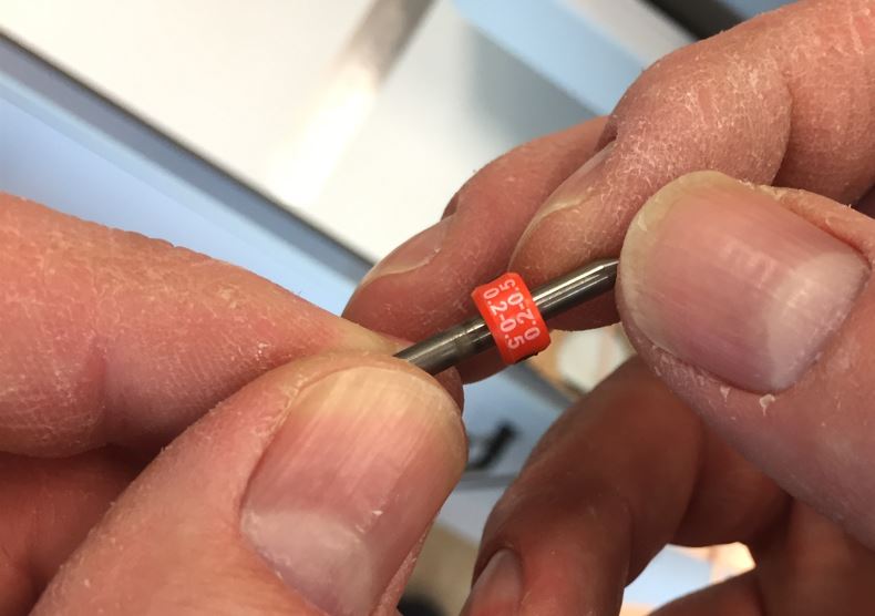
DRILLING spiral drill 1.5mm universal cutter 0.2mm (v-bit)
MILLING (Biggest to smallest tool)
End mill 3 mm End mill 2 mm End mill 1 mm End mill 0.8mm
spiral drill 2 mm contour router 2 mm
step1:3mm for removing a lot of material.
step2: 2mm to follow the bounderies.
step3: 1mm between step 1 and 2
step 4: 0.8mm in the gap between bigger lines.
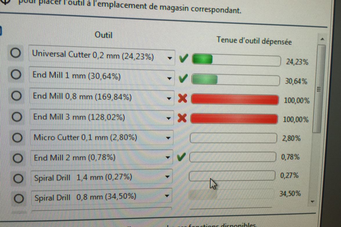
 The machine measure exactly each tool, we know their timelife.
 The material is stuck to the bed of the machine.
On-going videos
probing tools:
milling process
finishing step:
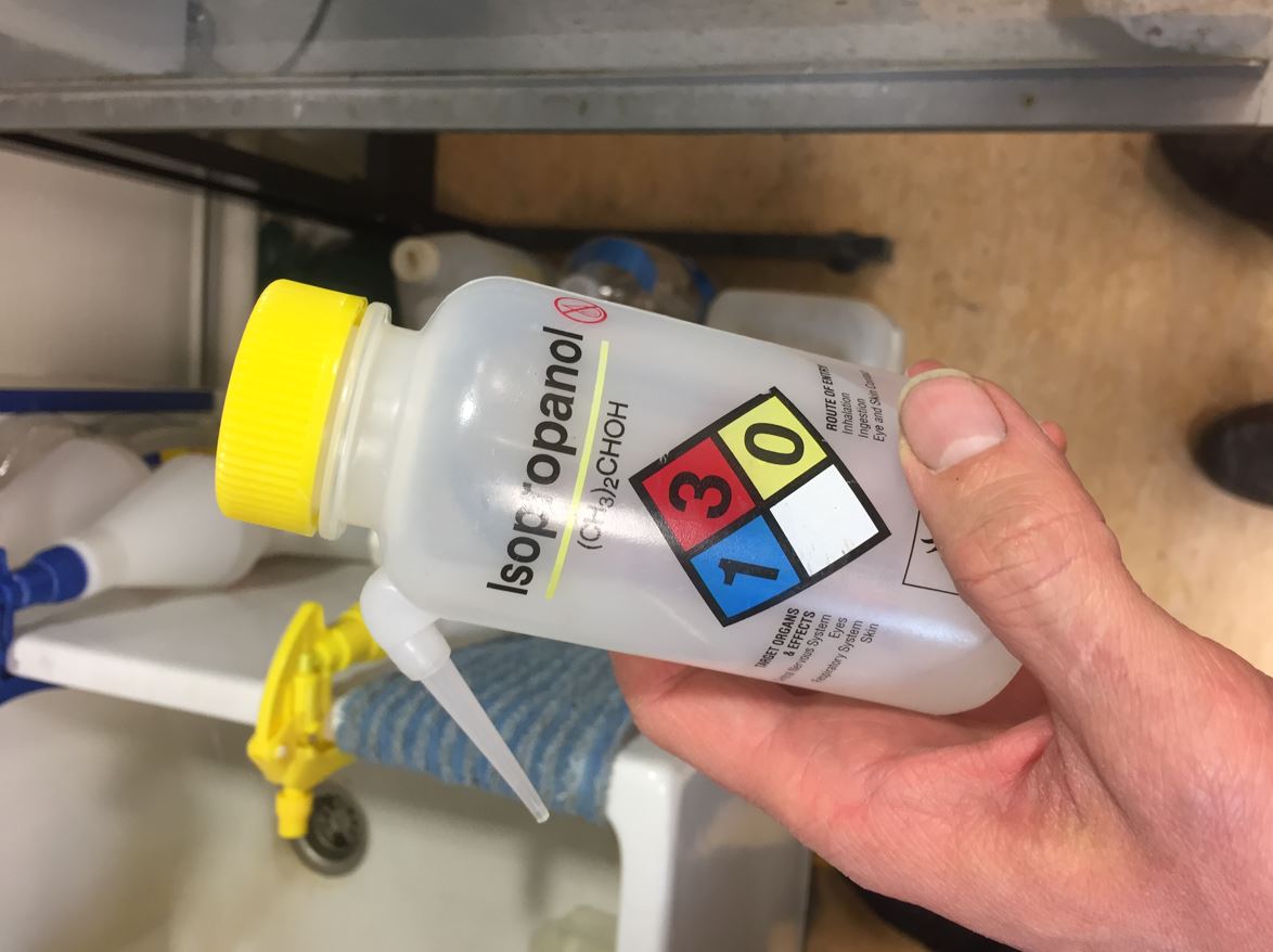
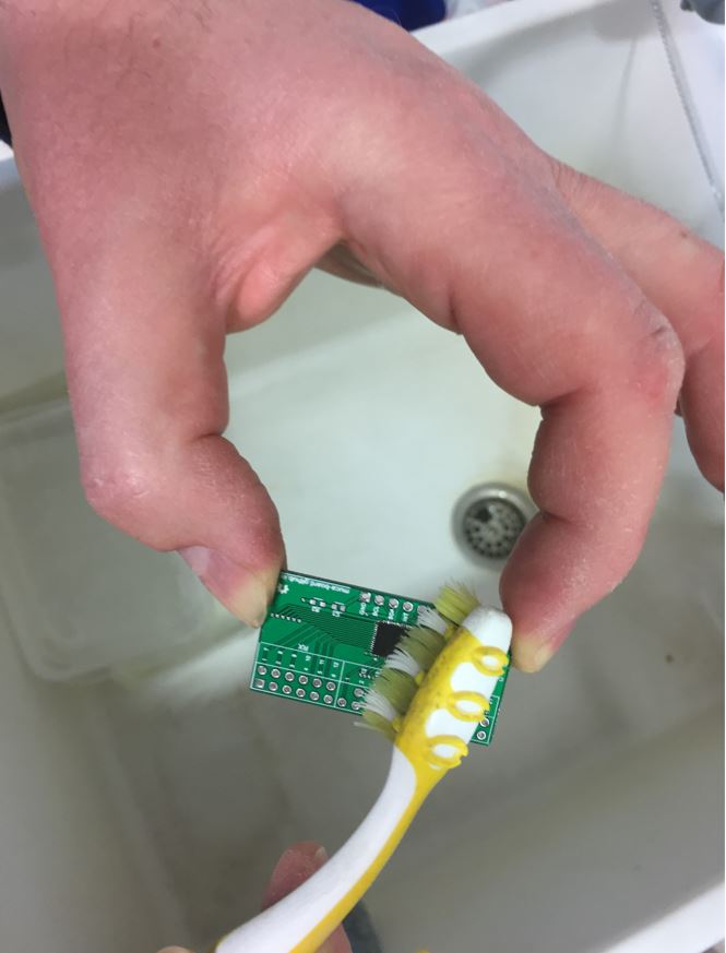
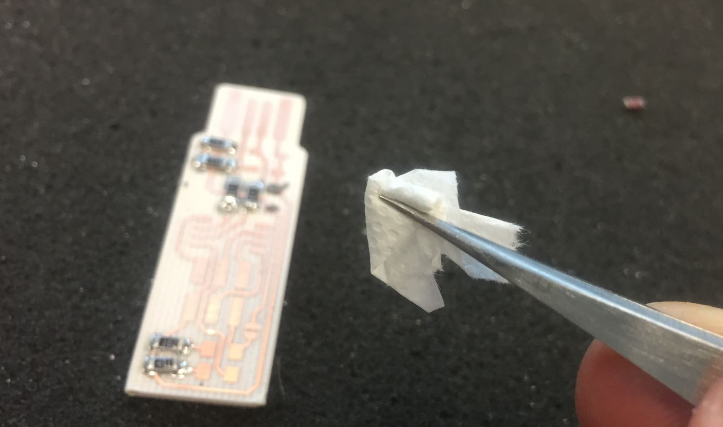
 To get the board cleaned, you can use an eraser.
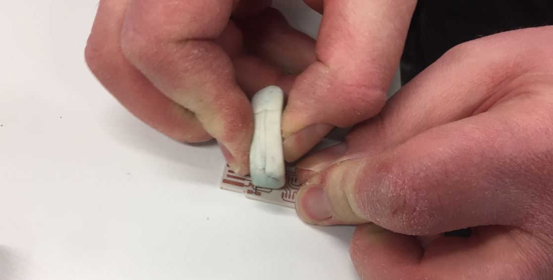 Next you use isopropanol and a teethbrush to make it very cleaned.
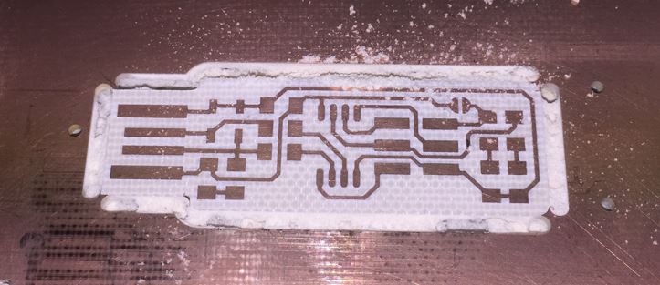
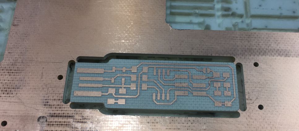
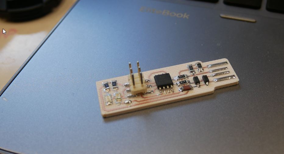
 The board is born.
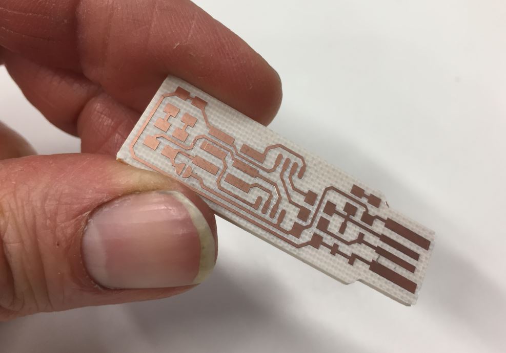
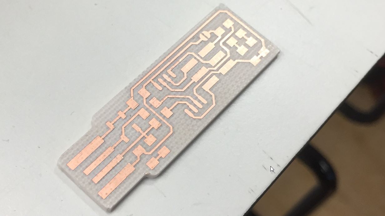
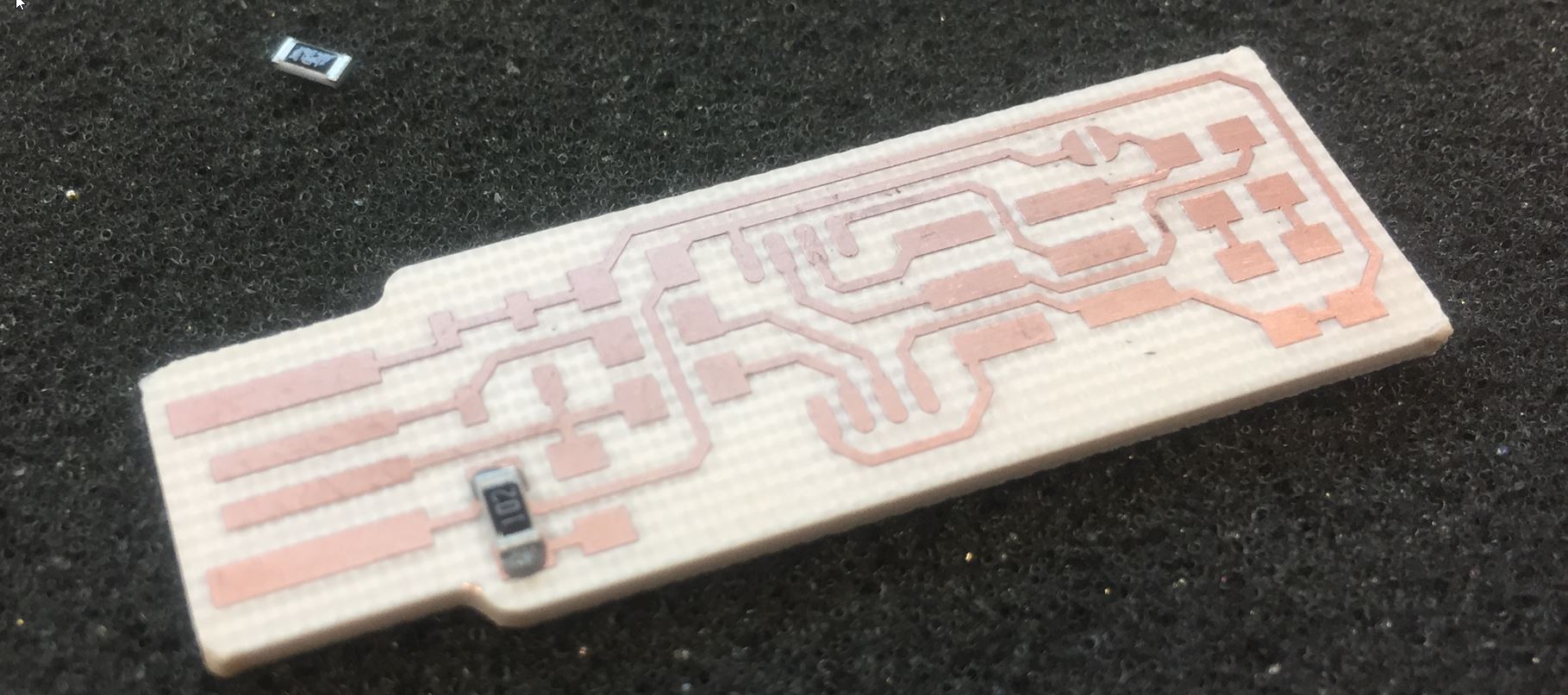
FABISP milling board.
Weller WD1 Digital 85W Soldering Station Power Unit, 120V
Technical Specifications:
Voltage: 120 V (input); 24 V (output)
Footprint: 5.27" x 4.25" x 5.77" (134 x 108 x 147 mm)
Power consumption: 85W
Temperature range: 150° F - 850° F (50° C - 450° C)
ESD safe: Yes
Temperature accuracy: ± 9° F (± 5° C)
Temperature stability: ± 10° F (± 6° C)
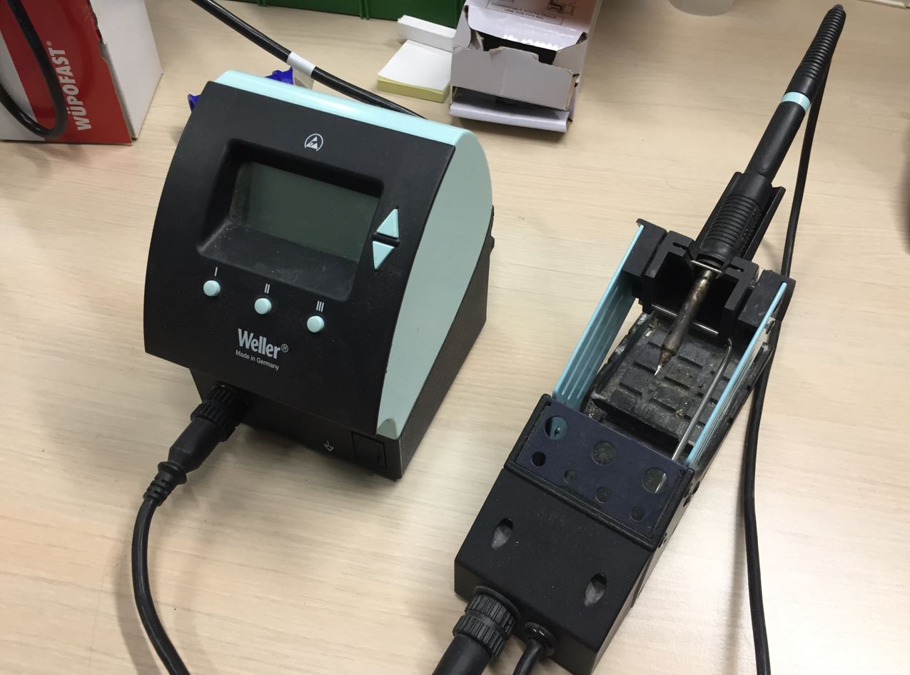
I use 97% STAIN COPPER SILVER wire, soldering temperature 340°C
SN100C- SnCu0,7Ni. Leadfree.
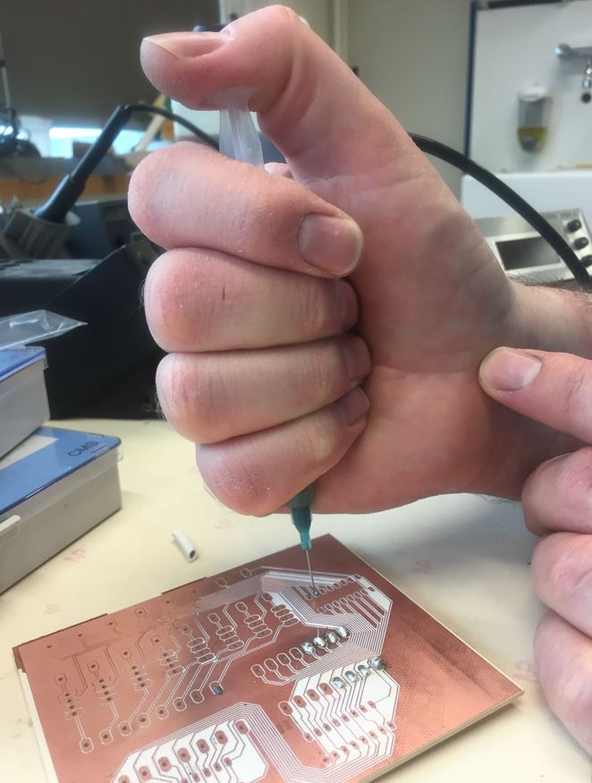
Vaccuum
Always working with a vaccuum up to your works!!
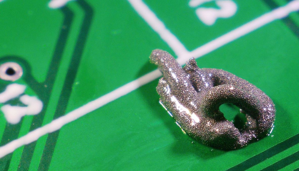
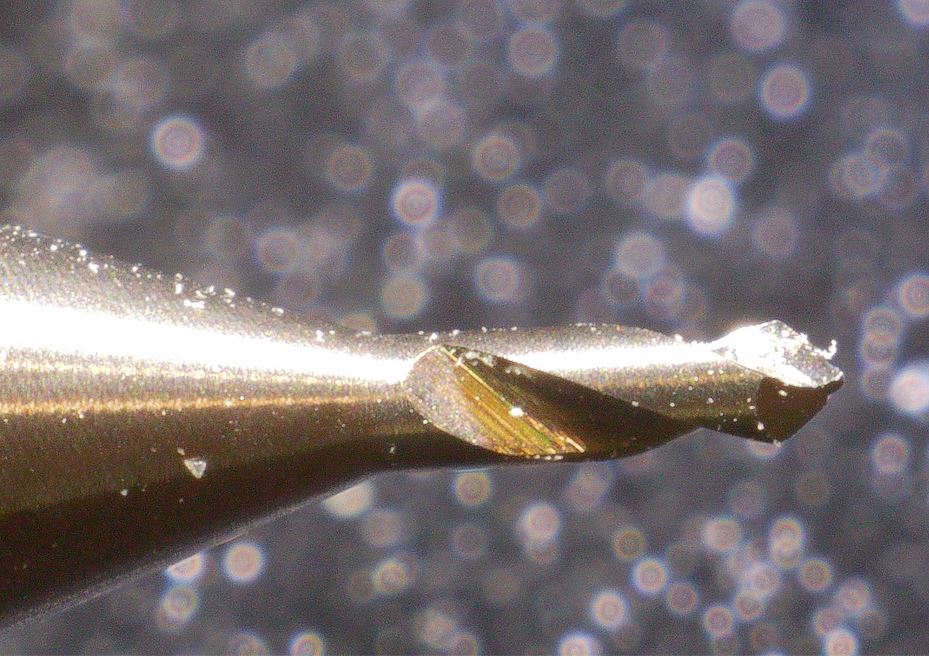
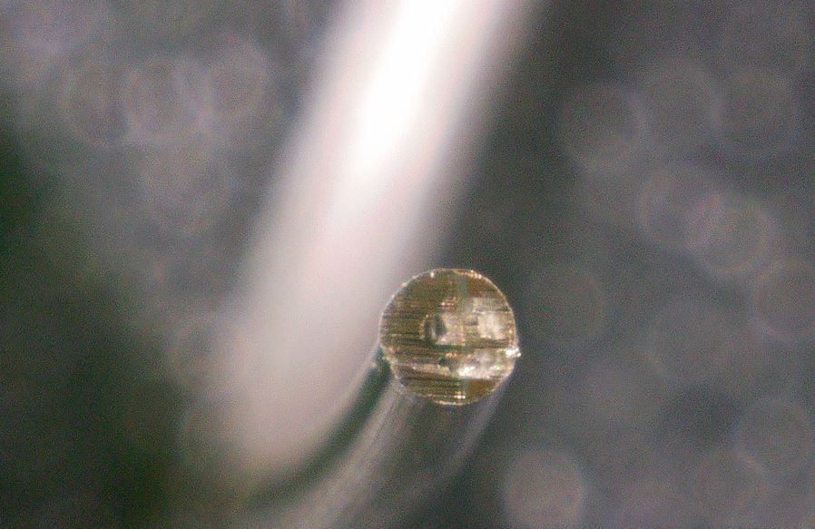
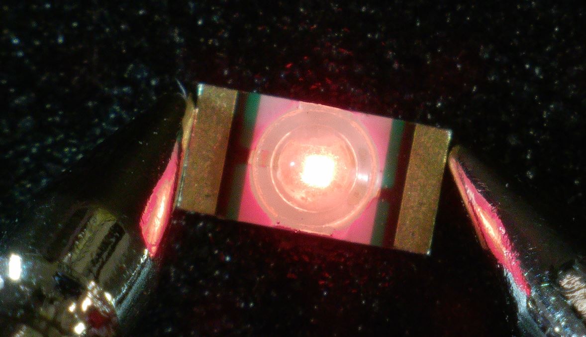
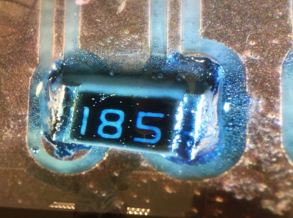
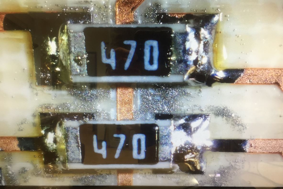
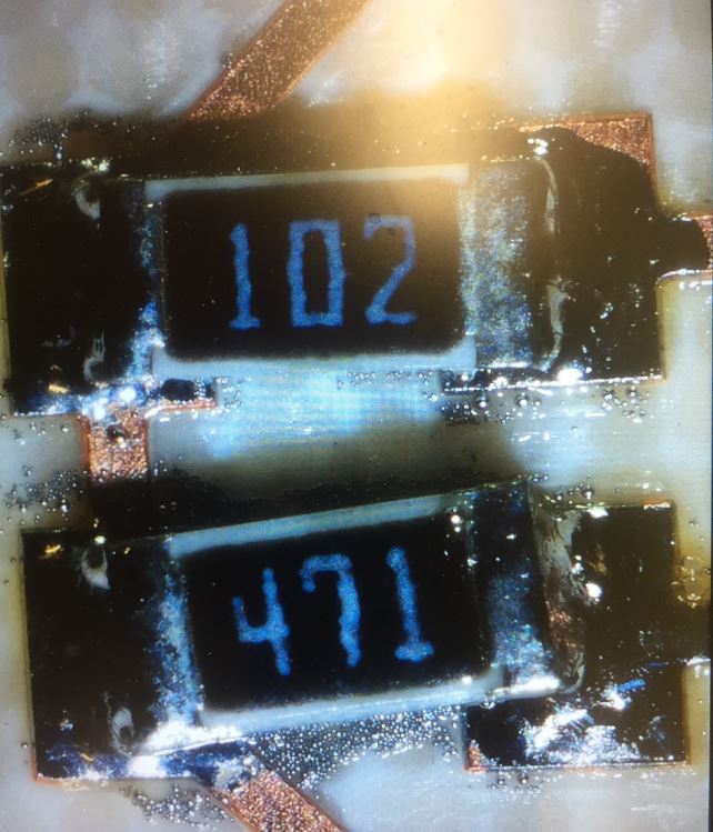
Microscope.
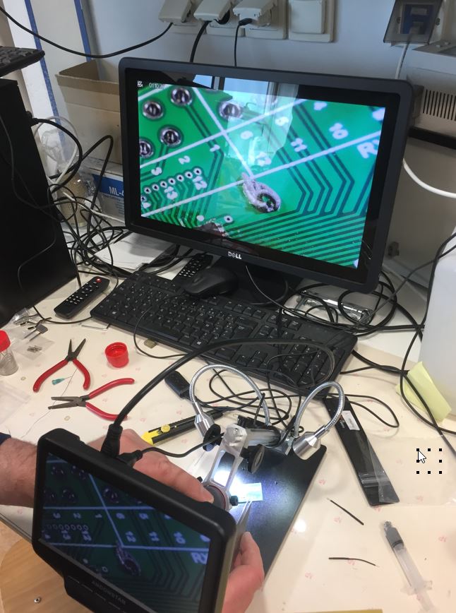
Here come some examples:
oven
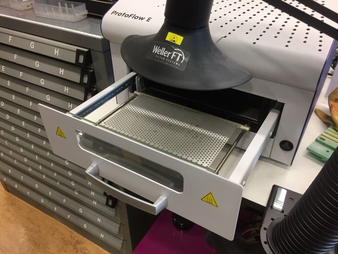 By using stings, it is easy to solder after the Easy to use with the pasta stings.
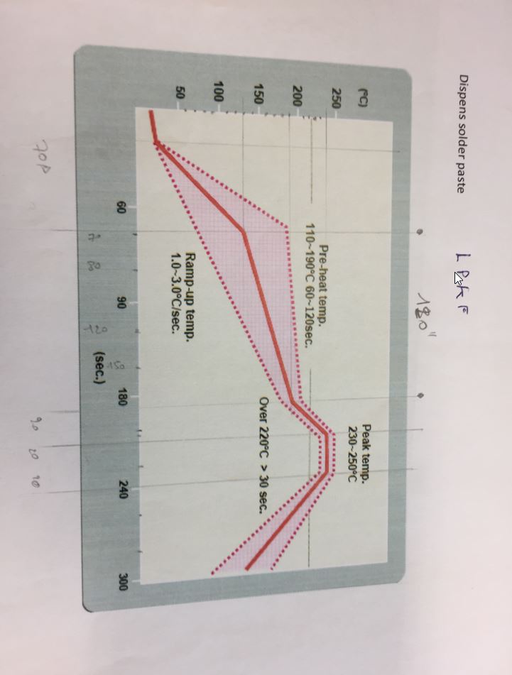 We made a try by brazing with brazing pasta(40% lead /60% stain) There is some resin called flow which prepares the soldering by cleaning at 150°c.
It increases gently 1 degree/second.
At 183°C, the state is becoming from solid to doughty.
At 220°c, the reflow is beginning, by decreasing 1°c/second.
We made a try by brazing with brazing pasta(40% lead /60% stain) There is some resin called flow which prepares the soldering by cleaning at 150°c.
It increases gently 1 degree/second.
At 183°C, the state is becoming from solid to doughty.
At 220°c, the reflow is beginning, by decreasing 1°c/second.
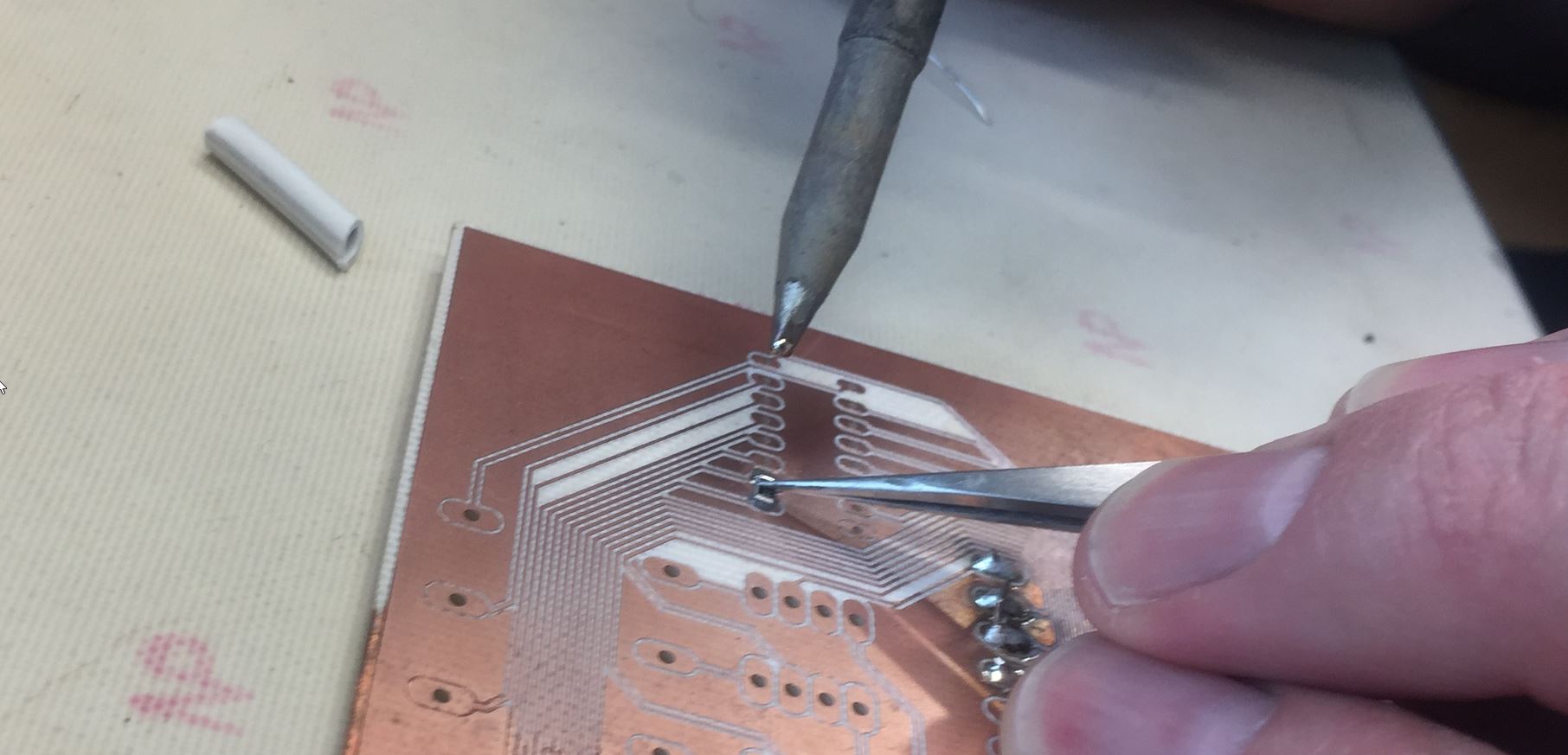
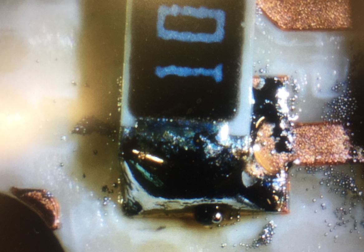
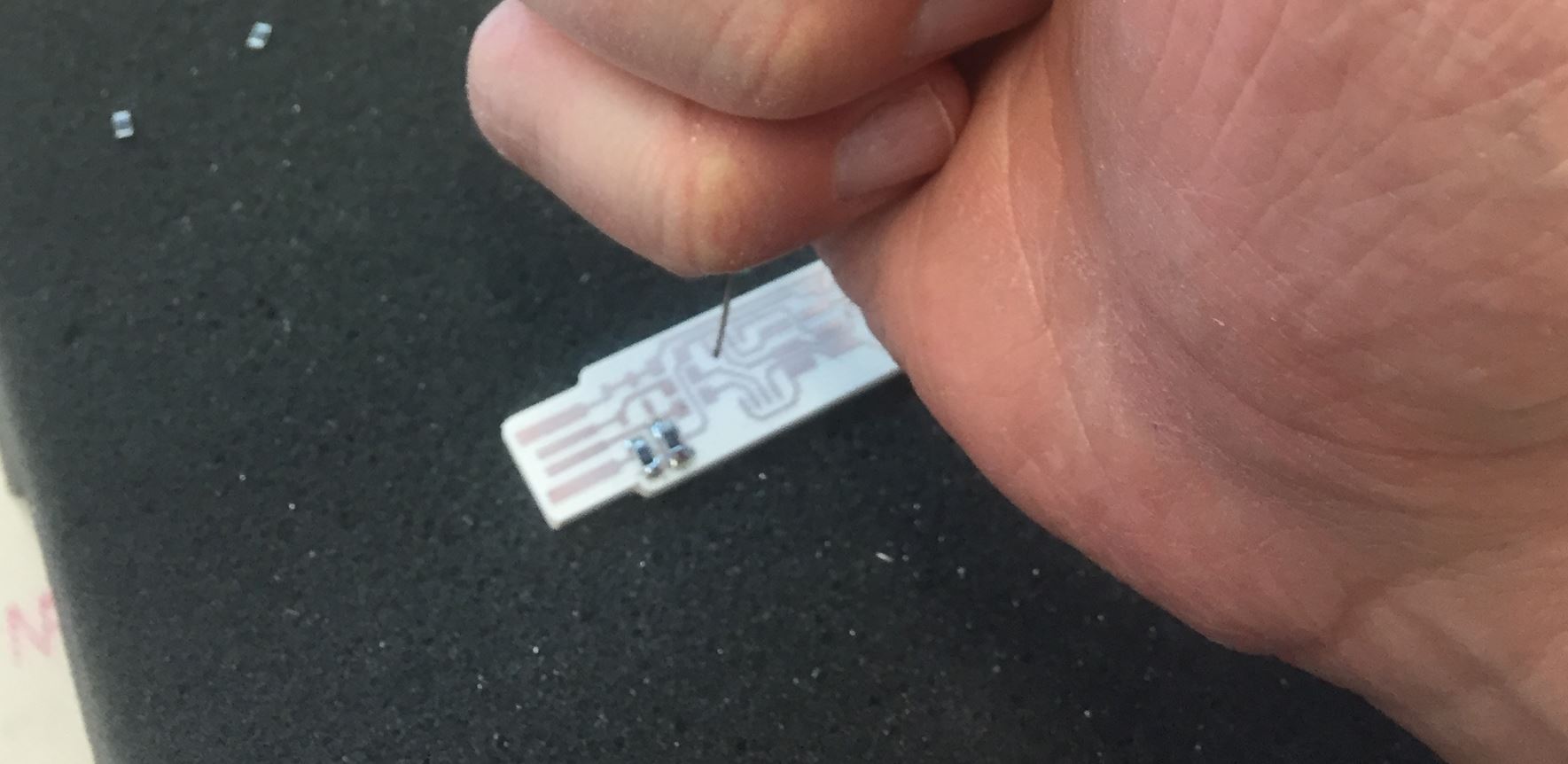
Soldering

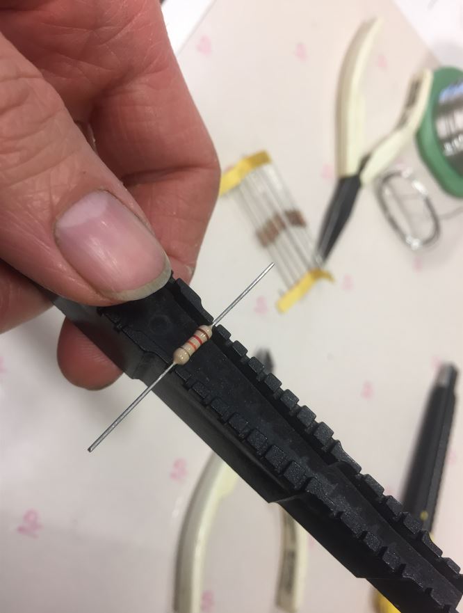
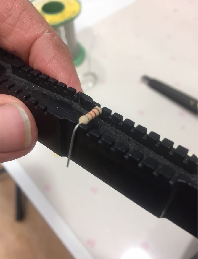
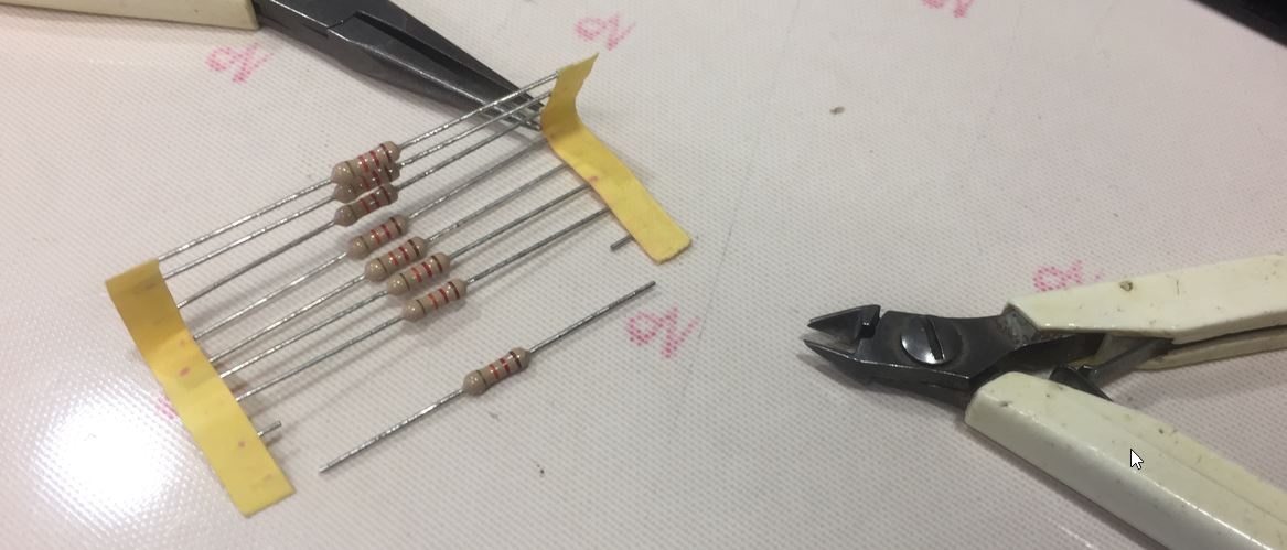
Thierry showed me some interesting tools such as this resistor bender.
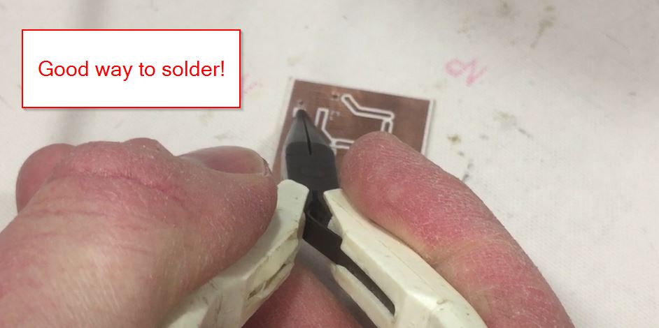
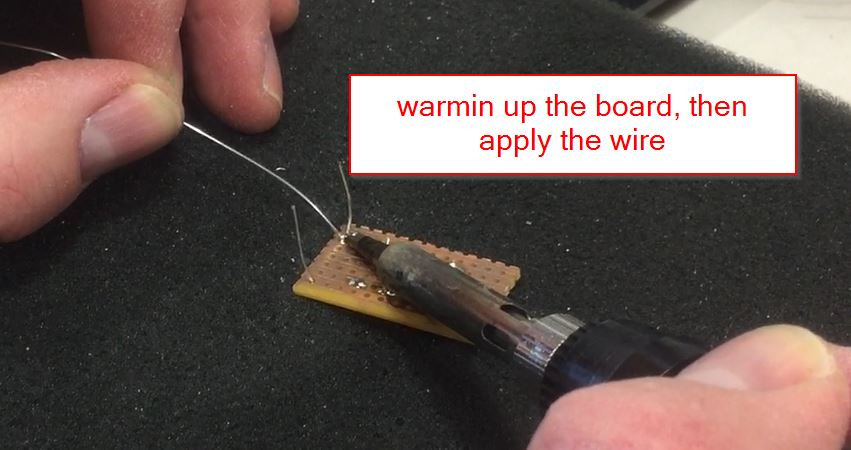
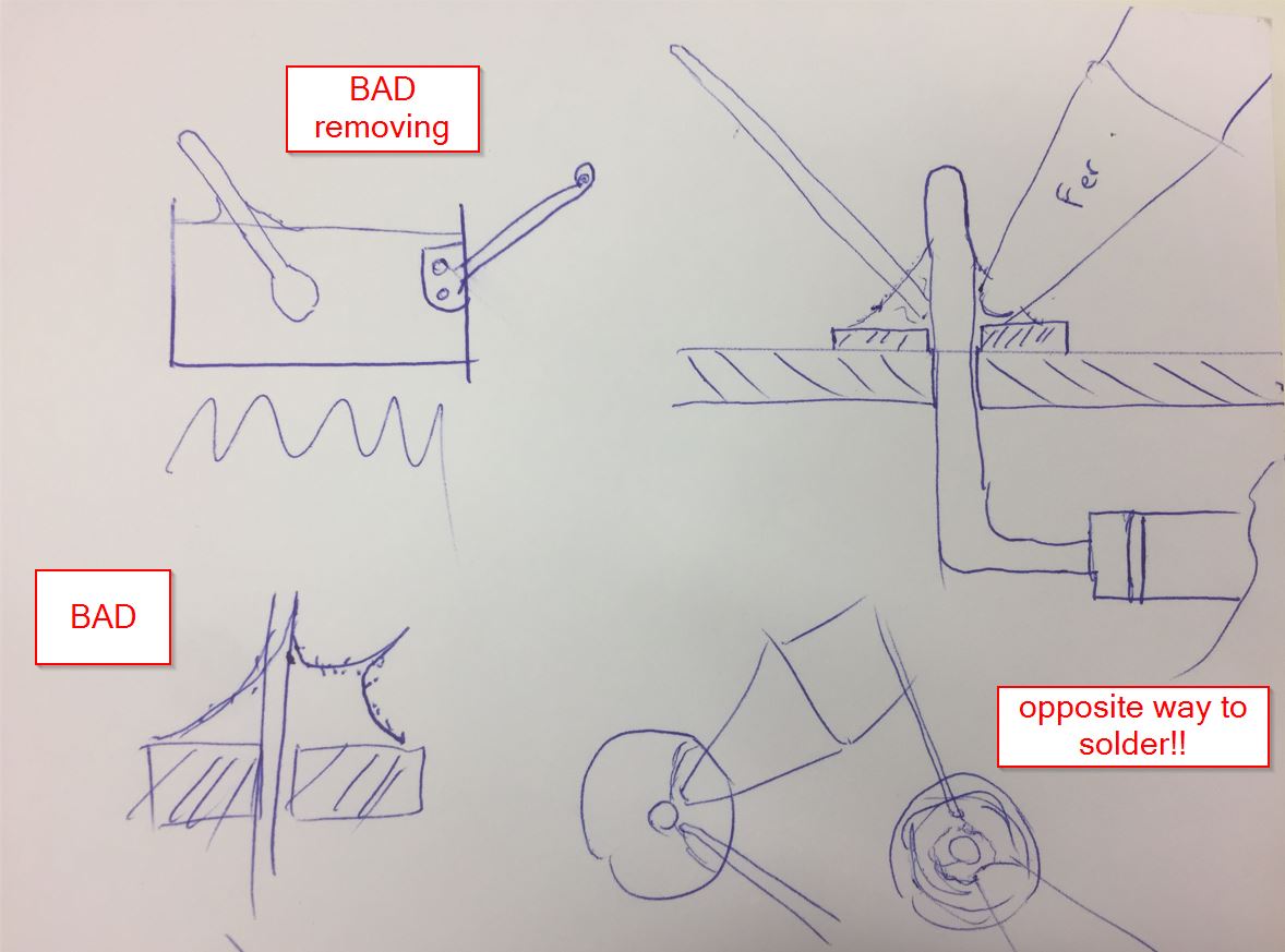
 Good moves for soldering.
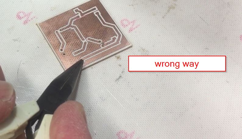 Better to be close the trace
When soldering, always take care of the ground position.
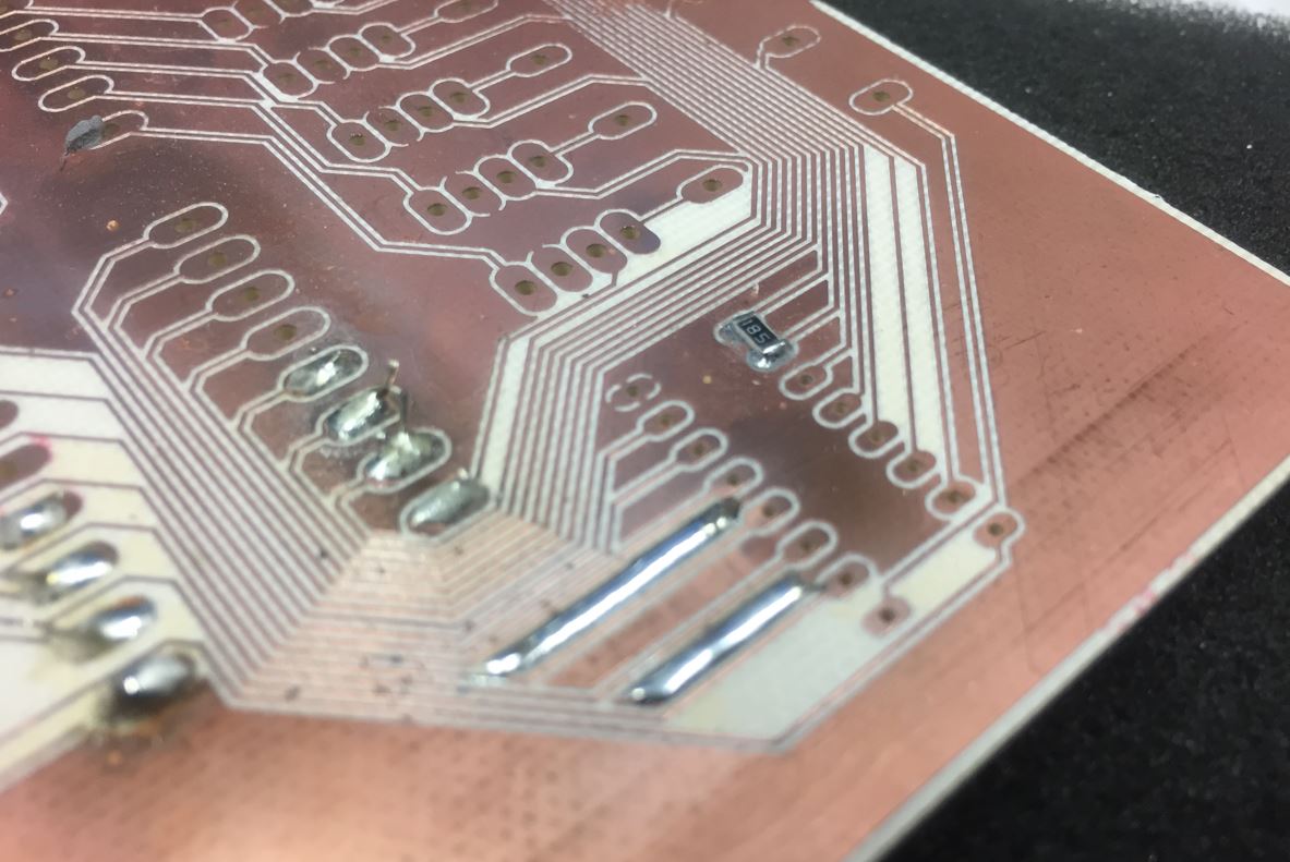
This « wrong way » can provide bridges to the ground.
Short circuit.
Use some foam, it helps you to rotate your board.
Better to be close the trace
When soldering, always take care of the ground position.
This « wrong way » can provide bridges to the ground.
Short circuit.
Use some foam, it helps you to rotate your board.
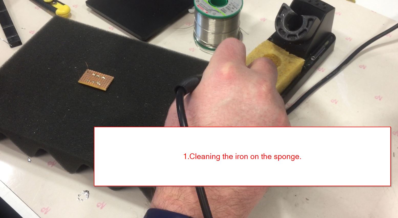
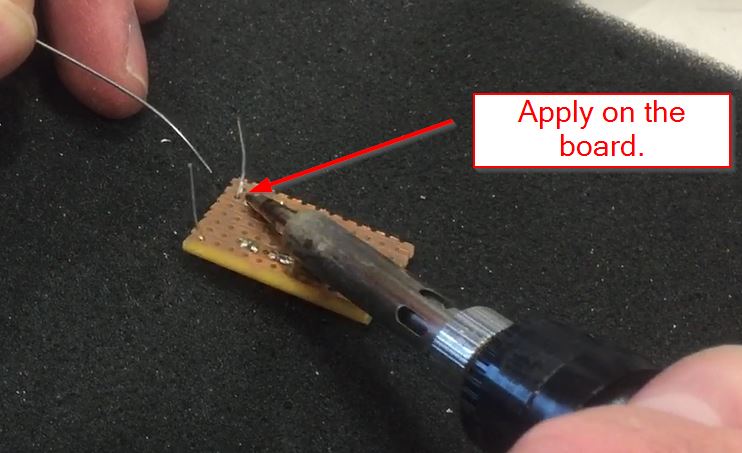
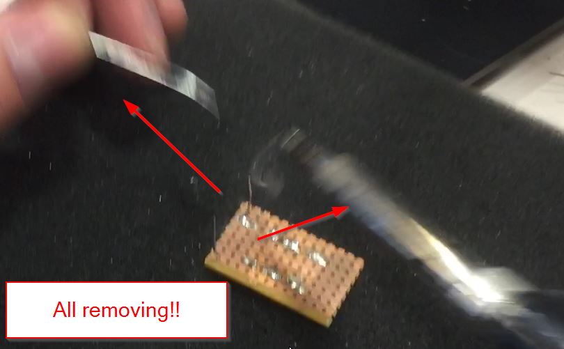
 2 seconds of soldering.
programming the programmer:
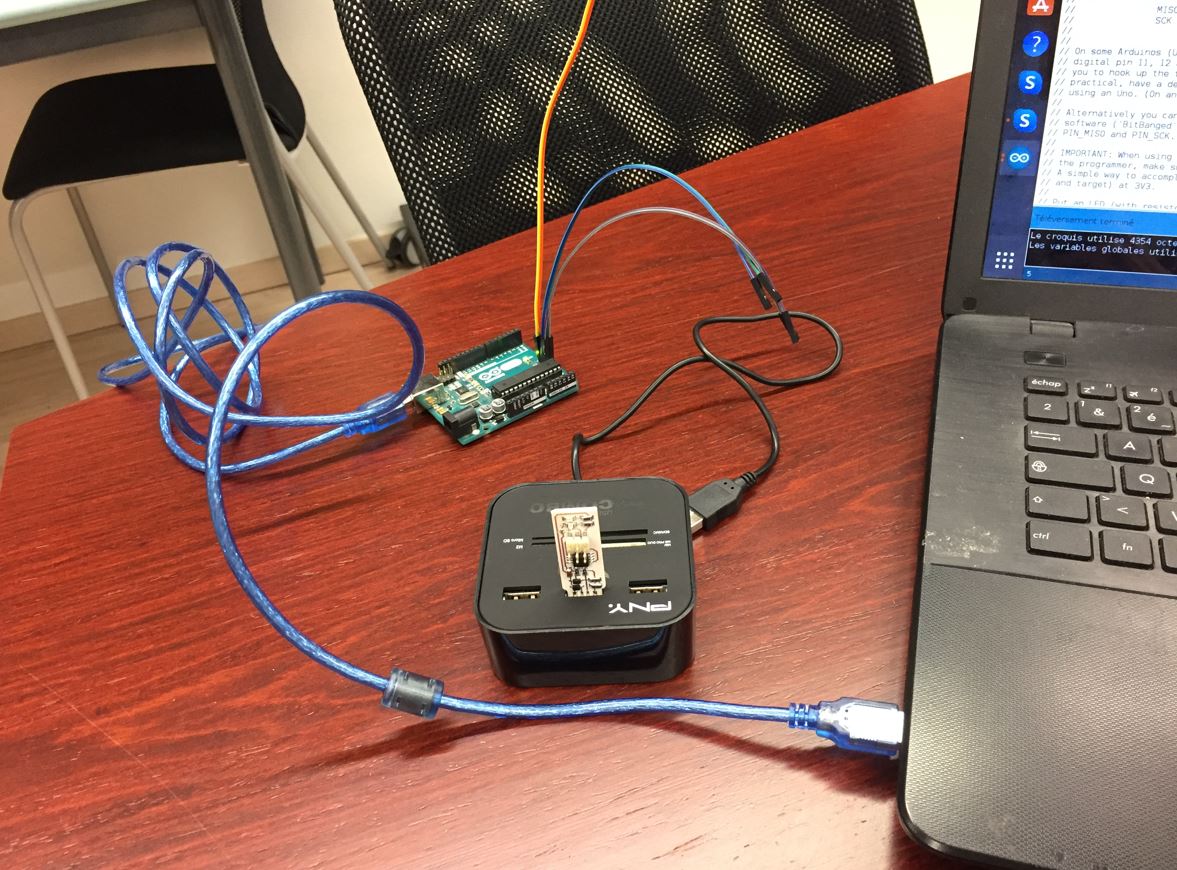
I have followed the tutorial to use Arduino as an ISP from Fabacademy tutorials.
http://pub.fabcloud.io/tutorials/week04_electronic_production/arduino_isp.html